A normal metal tunnel-junction heat diode
Abstract
We propose a low-temperature thermal rectifier consisting of a chain of three tunnel-coupled normal metal electrodes. We show that a large heat rectification is achievable if the thermal symmetry of the structure is broken and the central island can release energy to the phonon bath. The performance of the device is theoretically analyzed and, under the appropriate conditions, temperature differences up to 200 mK between the forward and reverse thermal bias configurations are obtained below 1 K, corresponding to a rectification ratio 2000. The simplicity intrinsic to its design joined with the insensitivity to magnetic fields make our device potentially attractive as a fundamental building block in solid-state thermal nanocircuits and in general-purpose cryogenic electronic applications requiring energy management.
The evolution of modern electronics has been boosted by the introduction of non-linear elements like diodes and transistors. The latter represented fundamental milestones for the control of electric currents and for the execution of logic operations in contemporary electronic devices. On the other hand, in the last decade we witnessed an explosion of interest in the investigation of thermal transport at the nanoscale. GiazottoRev ; Dubi ; LiRev ; BenentiRev Although appearing more difficult to control, heat transfer in solids embodies one of the most interesting and promising topics in nanoscience. Yet, the implementation of solid-state circuits that could enable the manipulation of heat currents is still at the earliest stage of development. These structures would be at the basis of emerging fields such as nanophononics,LiRev thermal logic LiRev and coherent caloritronics.GiazottoNature ; MartinezNature ; MartinezRev Moreover, they would be of great conceptual and technological interest for many other research fields such as solid-state cooling,GiazottoRev ; GiazottoTaddei ultrasensitive cryogenic radiation detection GiazottoRev ; GiazottoHeikkila and quantum information.NielsenChuang ; SpillaArxiv In this context, the realization of highly-efficient thermal diodes, i. e., devices in which thermal transport along a specific direction is dependent upon the sign of the temperature gradient,Starr ; RobertsRev appears as a crucial first step.
So far, several proposals have been made to design thermal rectifiers dealing, for instance, with phonons,Terraneo ; Li ; Segal ; Segal2 electrons GiazottoBergeret ; MartinezAPL ; Ren ; Ruokola1 ; Kuo ; Ruokola2 ; Chen and photons.BenAbdallah On the experimental side, encouraging results were obtained in devices that exploited phononic Chang ; Kobayashi ; Tian or electronic Scheibner thermal currents. In the latter case, a large rectification effectiveness has been demonstrated very recently in a hybrid superconducting device at cryogenic temperatures.MartinezArxiv
In this Letter we propose and theoretically analyze the performance of a thermal diode consisting of three normal metal islands (N1, N2, and N3) connected by two thin insulating layers (I), thereby forming a N1IN2IN3 junction. As we shall argue, this simple design can offer outstanding rectification effectiveness at low temperatures (below 1 K), provided that two conditions are satisfied: (i) the thermal symmetry of the system must be broken, and (ii) N2 must be coupled to the phonon bath. The proposed device could be easily realized with conventional nanofabrication techniques GiazottoNature ; MartinezNature ; MartinezArxiv and could be immediately exploited in low-temperature solid-state thermal circuits. Moreover, it would be virtually unaffected by magnetic fields ensuring high performance also in conditions where a hybrid superconducting thermal diode MartinezArxiv could lose its effectiveness.

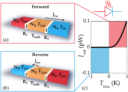
We shall start, first of all, by defining two parameters that will help us to describe the diode’s performance, i.e., the rectification effectiveness and the thermal efficiency . Toward this end, we analyze in more detail the structure of our system. As shown in Fig. 1(a) and 1(b), N2 is coupled to N1 and to N3 by means of two tunnel junctions characterized by resistances and , respectively. For simplicity, from now on, we will set and consider only the parameter , accounting for the asymmetry of the device. N1 and N3 act as thermal reservoirs and are used to establish a temperature gradient across the device. Electrode N2, instead, represents the core of the diode, since it controls the heat flow from a reservoir to the other by releasing energy to the phonon bath (residing at temperature ). In the forward configuration, the electronic temperature of N1 is set to . This temperature bias leads to heat currents and flowing into N2 and N3, respectively. On the other hand, in the reverse configuration the electronic temperature of N3 is set to , generating the heat currents and flowing into N2 and N1, respectively. Under these assumptions, we can define the rectification effectiveness as:
| (1) |
In general, a highly-effective thermal diode is characterized by or . In our case, since we have chosen , the forward configuration results to be the most transmissive, as we will show. The thermal diode’s response can be heuristically compared to that of the well-known electric diode by plotting the output current vs. the bias temperature . In the forward configuration we define and , whereas in the reverse configuration and . As shown in Fig. 1(c), if the behavior of vs. is strongly asymmetrical, indicating a drastic mismatch of the diode’s heat transport properties between the forward and the reverse configuration. Yet, another important parameter that has to be considered is the thermal efficiency. In the transmissive configuration, it can be defined as:
| (2) |
indicating the fraction of power that is transferred from N1 to N3. An ideal diode should exhibit and , leading to and .
We describe now the equations governing heat transport in our device. First, if we consider two N electrodes residing at electronic temperatures and (with for definiteness) coupled by means of a tunnel junction, the stationary electronic thermal current flowing through the junction can be written as:GiazottoBergeret
| (3) |
where is the contact resistance, is the electron charge and is the Boltzmann’s constant. Moreover, we must take into account the heat exchanged by electrons in the metal with lattice phonons:MartinezNature ; Maasilta
| (4) |
Here is the material-dependent electron-phonon coupling constant, is the volume of the electrode and is the characteristic exponent of the material. In this work we will consider two materials that are commonly exploited to realize N electrodes in nanostructures, i.e., copper (Cu) and manganese-doped aluminum (AlMn). The former is typically characterized by WK-5m-3 and ,GiazottoRev ; GiazottoNature while the latter exhibits WK-6m-3 and .MartinezNature ; MartinezArxiv Furthermore, we assume that N1 and N3 are identical, with volumes m-3.MartinezArxiv

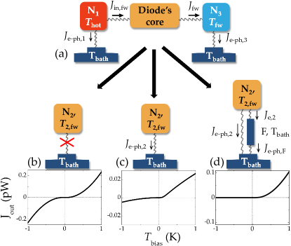
Equations 3 and 4 can be used to formulate a thermal model accounting for heat transport through the device. The model is sketched in Fig 2(a) and describes the forward temperature bias configuration, in which the electrodes of the chain reside at temperatures . Here, and represent the electronic temperatures of N2 and N3, respectively. The terms and account for the heat transferred from N1 to N3. The reservoirs can release energy to the phonon bath by means of and . Photon-mediated thermal transport, MeschkeNature ; Schmidt ; Pascal owing to poor impedence matching, as well as pure phononic heat currents are neglected in our analysis.GiazottoNature ; MartinezNature ; MartinezArxiv We can now write a system of energy-balance equations that account for the detailed thermal budget in N2 and N3 by setting to zero the sum of all the incoming and outgoing heat currents:
| (5) |
Here is the heat current that flows from N2 to the phonon bath. Since the rectification effectiveness is defined under the condition of equal temperature bias in both the configurations, in Eqs. 5 we set and as independent variables and we calculate the resulting and . Another system of energy-balance equations can be written and solved for the reverse configuration,reverse in which N2 and N1 reach electronic temperatures and , respectively. Finally, we can extract the values of and .
We discuss in the following the crucial role of N2, which is the core of the proposed thermal diode. Figures 2(b), 2(c) and 2(d) display three possible designs of the central electrode. It is illustrative to start with the simplest one, at least conceptually, consisting of an island perfectly isolated from the phonon bath [see Fig. 2(b)]. In this case, the term is null and from the energy-balance equations we obtain:
| (6) | ||||
| (7) |
Then, since by assumption we set and , we have and we can easily show that the rectification efficiency becomes:
| (8) |
for every value of . This means that in this system no rectification occurs regardless the asymmetry of the coupling between N2 and the reservoirs. As a confirmation of the latter result, the lower panel of Fig. 2(b) displays the symmetrical behavior of vs. , calculated for 100.
In order to envision a device exhibiting a sizable thermal rectification, it is useful to rewrite as the following condition for temperatures:
| (9) |
where and the mean temperatures . Expression 9 indicates a simple approach to pursue our goal: in the reverse configuration the electronic temperatures of N1 and N2 must be similar and close to the lowest temperature in the system, i.e., . This condition can be satisfied by setting and by coupling N2 to the phonon bath. In this way, reduces heat transfer to N2, which is able to release energy to the bath, thereby lowering both and . On the other hand, the coupling between N2 and the phonon bath should have a limited impact on heat transport in the forward configuration.
Figures 2(c) and 2(d) show two possible designs that allow to create a thermal link between N2 and the phonon bath. The former just exploits the natural coupling between electrons and lattice phonons in metals, while the latter requires an additional N electrode labeled F, acting as a thermalizing cold finger. To this end, F must be tunnel-coupled to N2 (with a resistance ) and must reside at . We shall demonstrate that the second option provides the best rectification performance, as shown by the dependence of on in the lower panels of Fig. 2(c) and 2(d). The former curve is calculated for and m-3, while the latter is obtained for , m-3 and .

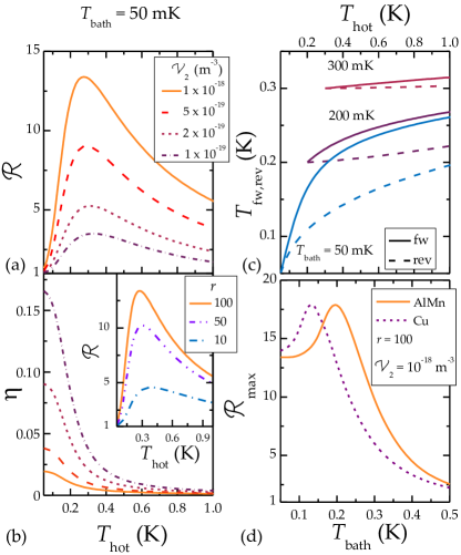
We focus first on the design sketched in Fig. 2(c), which corresponds to setting the term in the energy-balance equations. Figure 3(a) and 3(b) show respectively the behavior of and vs. in an AlMn device for different values of at mK and for . The rectification effectiveness exhibits a non-monotonic trend that reaches a maximum value () around mK, whereas has a maximum at and monotonically approaches zero at larger temperatures. The inset of Fig. 3(b) displays as a function of for different values of the resistance asymmetry and for m-3. It appears evident how increasing and generate larger values of but gradually suppress the thermal efficiency. Furthermore, the latter parameter clearly indicates that the influence of the electron-phonon coupling increases with temperature (see Eq. 4), causing strong energy losses in both the configurations. This can be noted also in Fig. 3(c), which displays the output temperatures and vs. of a diode with m-3 and for three representative values of . In particular, the derivatives of and strongly decrease as and increase, pinpointing a reduction in the thermal efficiency of the device. Moreover, we also notice that at low the electron-phonon coupling is not much effective in lowering and . This effect is highlighted in Fig. 3(d), which compares the dependence on for two devices made of AlMn and Cu. In the AlMn diode reaches a maximum value of at mK, which indicates the temperature where the electron-phonon coupling attains the highest effectiveness in lowering , while having limited repercussions on . On the other hand, in Cu follows a power law that leads to a shift of the peak to lower values of .

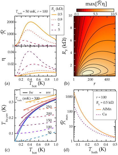
These results can be largely improved by tunnel-coupling the electrode F to N2, thereby creating an efficient channel through which the diode’s core can release energy. As sketched in Fig. 2(d), this can be taken into account by setting in the energy-balance equations. Figure 4(a) shows and vs. for different values of at mK. Remarkably, is obtained for , m-3 and . Similarly to the previous case, increasing and leads to a suppression of the thermal efficiency, which appears to be lower than that obtained above. Nevertheless, presents new important features: it has a non-monotonic behavior with a minimum at and a peak centered at a specific which depends on the parameters , and and can correspond to high values of . The low-temperature dependence is dominated by the F channel, which exchanges heat following a dependence. The influence of the cold finger gradually vanishes at larger temperatures and the electron-phonon coupling starts playing the most important role reducing . It is then clear how F is highly efficient in keeping close to and close to zero, while attenuating its effect on that can reach relatively high temperatures. This mechanism allows us to decrease and consequently to reduce the influence of the electron-phonon coupling at high . By defining the global efficiency of the thermal rectifier , it is possible to determine the best parameters to optimize the diode’s performance. The contour plot shown in Fig. 4(b) highlights the dependence of the maximum value of on and , indicating the optimal working region of the proposed device. Figure 4(c) displays the rectifier’s output temperatures and vs. for and at different values of . The results point out a maximum difference of mK between the forward and reverse configurations at mK. Finally, Fig. 4(d) confirms the noxious effect of the electron-phonon coupling on the performance of the diode. As a matter of fact, the behavior of as a function of shows that the dependence of in Cu is extremely detrimental in the forward configuration and can reduce the rectification effectiveness up to a factor 10.
It is worth mentioning that adding a fourth electrode to the chain would allow us to obtain even when , provided that the coupling between the central islands and the phonon bath is asymmetrical. However, it turns out that this effect cannot improve the performance obtained with the chain made of three electrodes. As a matter of fact, the additional element in the diode’s core produces further energy losses and mitigates the temperature gradient , thereby reducing .
In summary, we have proposed and theoretically analyzed the performance of a thermal rectifier consisting of a simple NININ junction. We have demonstrated that a large rectification is achievable if the thermal symmetry of the system is broken and the central electrode is coupled to the phonon bath. Extremely high values of can be obtained if a cold finger is connected to the core of the rectifier, thereby creating an efficient channel through which the diode can release energy in the non-transmissive temperature bias configuration. The device could be easily implemented by standard nanofabrication techniques MartinezArxiv and, combined with heat current interferometers, GiazottoNature ; MartinezNature might become one of the building blocks of coherent caloritronic nanocircuits.GiazottoNature ; MartinezNature ; MartinezRev Moreover, its essential design and composition candidate our diode to become a promising tool for thermal management in general-purpose cryogenic electronic applications, even in presence of magnetic fields.
The Marie Curie Initial Training Action (ITN) Q-NET 264034 and the Italian Ministry of Defense through the PNRM project TERASUPER are acknowledged for partial financial support.
References
- (1) F. Giazotto, T. T. Heikkilä, A. Luukanen, A. M. Savin, and J. P. Pekola, Rev. Mod. Phys. 78, 217 (2006).
- (2) Y. Dubi and M. Di Ventra, Rev. Mod. Phys. 83, 131 (2011).
- (3) N. Li, J. Ren, L. Wang, G. Zhang, P. Hänggi, and B. Li, Rev. Mod. Phys. 84, 1045 (2012).
- (4) G. Benenti, G. Casati, T. Prosen, and K. Saito, arXiv:1311.4430.
- (5) F. Giazotto and M. J. Martínez-Pérez, Nature 492, 401 (2012).
- (6) M. J. Martínez-Pérez and F. Giazotto, Nat. Commun. 5, 3579 (2014).
- (7) M. J. Martínez-Pérez, P. Solinas, and F. Giazotto, J. Low Temp. Phys., 2014, 10.1007/s10909-014-1132-6.
- (8) F. Giazotto, F. Taddei, R. Fazio, and F. Beltram, Appl. Phys. Lett. 80, 3784 (2002).
- (9) F. Giazotto, T. T. Heikkilä, G. P. Pepe, P. Helistö, A. Luukanen, and J. P. Pekola, Appl. Phys. Lett. 92, 162507 (2008).
- (10) M. A. Nielsen and I. L. Chuang, Quantum Computation and Quantum Information (Cambridge University Press, 2002).
- (11) S. Spilla, F. Hassler, and J. Splettstoesser, arXiv:1311.7561.
- (12) C. Starr, J. Appl. Phys. 7, 15 (1936).
- (13) N.A. Roberts and D.G. Walker, Int. J. Therm. Sci., 50, 648 (2011).
- (14) L.-A. Wu and D. Segal, Phys. Rev. Lett. 102, 095503 (2009).
- (15) D. Segal, Phys. Rev. Lett. 100, 105901 (2008).
- (16) B. Li, L. Wang, and G. Casati, Appl. Phys. Lett. 88 (2006).
- (17) M. Terraneo, M. Peyrard, and G. Casati, Phys. Rev. Lett. 88, 094302 (2002).
- (18) F. Giazotto and F. S. Bergeret, Appl. Phys. Lett. 103, 242602 (2013).
- (19) M. J. Martínez-Pérez and F. Giazotto, Appl. Phys. Lett. 102, 182602 (2013).
- (20) J. Ren and J.-X. Zhu, Phys. Rev. B 87, 165121 (2013).
- (21) T. Ruokola and T. Ojanen, Phys. Rev. B 83, 241404 (2011).
- (22) D. M. T. Kuo and Y.C. Chang, Phys. Rev. B 81, 205321 (2010).
- (23) T. Ruokola, T. Ojanen, and A.-P. Jauho, Phys. Rev. B 79, 144306 (2009).
- (24) X.-O. Chen, B. Dong, and X.-L. Lei, Chin. Phys. Lett. 25, 8 (2008).
- (25) P. Ben-Abdallah and S.-A. Biehs, Appl. Phys. Lett. 103, 191907 (2013).
- (26) C. W. Chang, D. Okawa, A. Majumdar, and A. Zettl, Science 314, 1121 (2006).
- (27) W. Kobayashi, Y. Teraoka, and I. Terasaki, Appl. Phys. Lett. 95, 171905 (2009).
- (28) H. Tian, D. Xie, Y. Yang, T. L. Ren, G. Zhang, Y. F. Wang, C. J. Zhou, P. G. Peng, L. G. Wang, and L.T. Liu, Sci. Rep. 2, 523 (2012).
- (29) R. Scheibner, M. König, D. Reuter, A. D. Wieck, C. Gould, H. Buhmann, and L. W. Molenkamp, New J. Phys. 10, 083016 (2008).
- (30) M. J. Martínez-Pérez, A. Fornieri, and F. Giazotto, arXiv:1403.3052.
- (31) L. J. Taskinen and I. J. Maasilta, Appl. Phys. Lett. 89, 143511 (2006).
- (32) D. R. Schmidt, R. J. Schoelkopf, A. N. Cleland, Phys. Rev. Lett. 93, 045901 (2004).
- (33) M. Meschke, W. Guichard, J. P. Pekola, Nature 444, 187 (2006).
- (34) L. M. A. Pascal, H. Courtois, and F. W. J. Hekking, Phys. Rev. B 83, 125113 (2011).
- (35) Energy-balance equations for the reverse configuration can be easily obtained by replacing , , , and .