Observation of Quantum-Tunneling Modulated Spin Texture in Ultrathin Topological Insulator Bi2Se3 Films
Abstract
Understanding the spin-texture behavior of boundary modes in ultrathin topological insulator films is critically essential for the design and fabrication of functional nano-devices. Here by using spin-resolved photoemission spectroscopy with p-polarized light in topological insulator Bi2Se3 thin films, we report tunneling-dependent evolution of spin configuration in topological insulator thin films across the metal-to-insulator transition. We observe strongly binding energy- and wavevector-dependent spin polarization for the topological surface electrons in the ultra-thin gapped-Dirac-cone limit. The polarization decreases significantly with enhanced tunneling realized systematically in thin insulating films, whereas magnitude of the polarization saturates to the bulk limit faster at larger wavevectors in thicker metallic films. We present a theoretical model which captures this delicate relationship between quantum tunneling and Fermi surface spin polarization. Our high-resolution spin-based spectroscopic results suggest that the polarization current can be tuned to zero in thin insulating films forming the basis for a future spin-switch nano-device.
pacs:
73.61.-rA three-dimensional topological insulator (TI) is a non-trivial phase of matter which acts as an electrical insulator in the bulk but can conduct a spin-polarized current on the surface Moore Nature insight ; Zahid ; Zhang ; Fu Liang PRB topological invariants ; David Nature BiSb ; Matthew Nature physics BiSe ; YLChen ; SCZhang ; David Nature tunable ; SCZhang1 ; TCI ; QiKunXue ; SmB6_Hasan ; Sakamoto ; Tjernberg ; SbTe ; Ando ; Neupane ; QKXue . These topological surface states are characterized by a Dirac cone-like energy-momentum dispersion relation. The novel electronic structure of TIs can be manipulated to realize various novel quantum phenomena such as spin-galvanic effects, dissipationless spin currents or neutral half-fermions for quantum information storage devices Galvanic effect ; Qi Science Monopole ; Essin PRL Magnetic ; Yu Science QAH ; Liang Fu PRL Superconductivity ; Linder PRL Superconductivity . The magnitude and wavevector dependence of the spin polarization of electrons and holes are among the most important key ingredients in considerations for the design of any functional device. However, such developments have been limited due to the residual bulk conductance in currently available materials which overwhelms the surface contribution. Additionally, scattering from the extrinsic bulk states leads to the reduction of spin polarization of the surface states. One promising route to minimize bulk conductance and thus improve effective spin polarization is to work with ultrathin films where the surface to volume ratio is significantly enhanced Linder ; HZLu and surface current can potentially dominate. On the other hand, in this limit the desired spin polarization of the surface states is kinematically reduced near the metal-to-insulator transition in the ultrathin films where the spin behavior is not known to this date QiKunXue ; Sakamoto ; Tjernberg ; QKXue ; SbTe .
To date, no systematic spin-sensitive spectroscopic experimental study has been reported in the ultrathin limit across the metal-to-insulator transition despite the direct relevance of spins in ultrathin film limits for nano-device fabrication as well as the potential discovery of novel topological phenomena. Studying the spin polarization in the ultra-thin limit is further important to experimentally demonstrate the theoretically predicted tunable Berry’s phase in TI thin films loca . Systematic mapping of the surface spin texture in energy, momentum space and its thickness dependence is essential to understand and interpret many transport experiments on thin film TIs that are of core interest in the current TI research. We report a systematic spin-resolved angle-resolved photoemission spectroscopy (SR-ARPES) and spin-integrated ARPES measurements on ultrathin Bi2Se3 thin films for the first time. Our measurements reveal that the spin polarization is large for larger wavevectors, and the polarization magnitude increases with reduced tunneling, and its magnitude saturates to the bulk limit at a faster rate at large electron momenta.
We observe strongly binding energy- and wavevector-dependent spin polarization for the topological surface electrons in the ultra-thin gapped- Dirac-cone limit, which experimentally shows that the Dirac gap opening and the thickness-dependent topological phase transition are a result of the quantum tunneling between the two oppositely spin-textured topological surface states. These unique spin features of ultrathin films, evidently distinct from the 3D TI, open up new possibilities for devices not possible with bulk topological insulators.
Results
Sample characterization
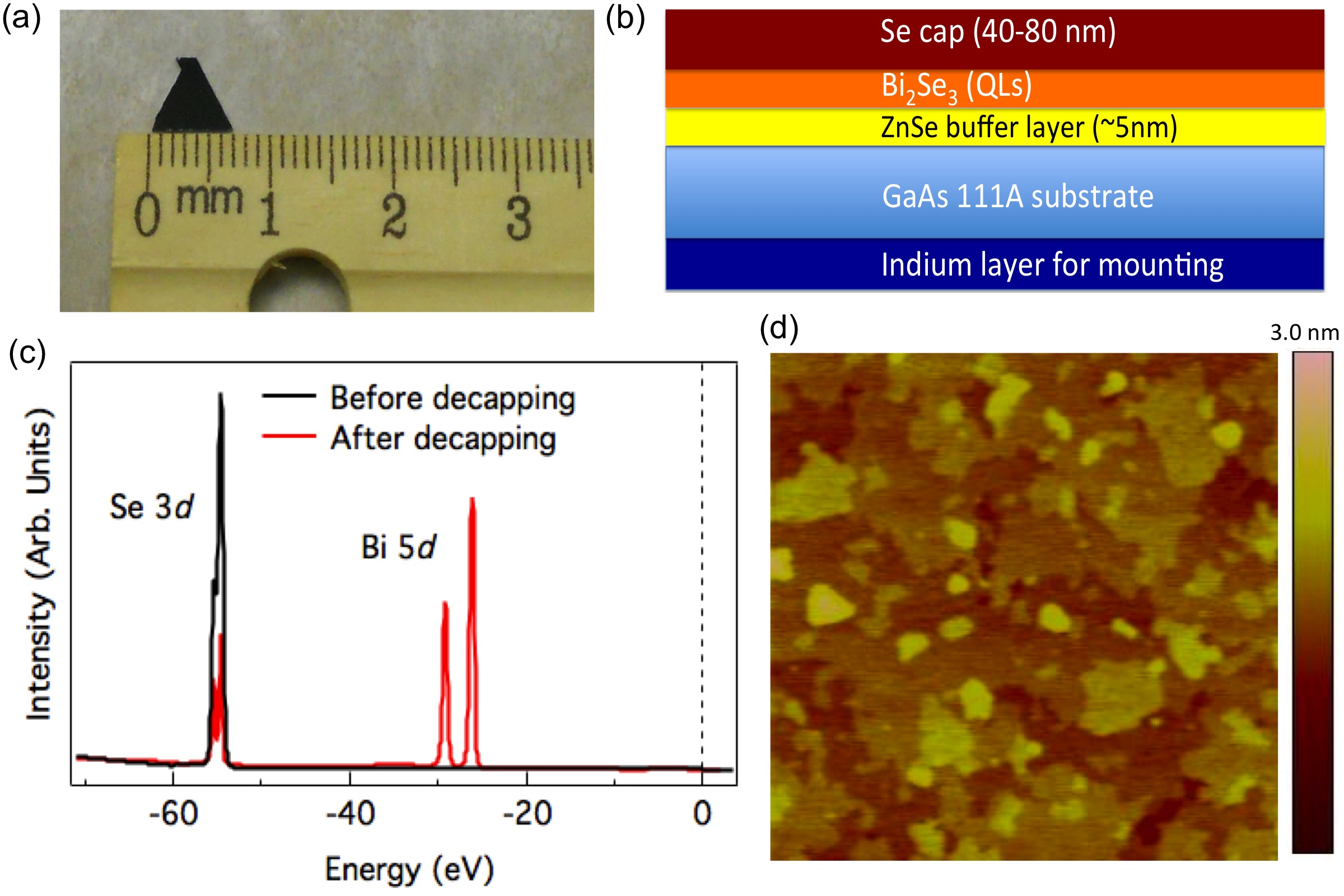
Spectroscopic measurements were performed on large ultrathin Bi2Se3 films prepared by the Molecular Beam Epitaxy (MBE) method on GaAs(111)A substrates (Fig. 1a). Each crystal layer of Bi2Se3 constitutes of five atomic layer, namely Se-Bi-Se-Bi-Se, which is called quintpule layer (QL) with the thickness of approximately 1 nm Matthew Nature physics BiSe . Our MBE films grow in a self-organized quintuple-layer by quintuple-layer mode, and high quality atomically smooth film can be obtained with the desired thickness (also see Supplementary Figures 1-7 and Supplementary Notes 1-3). A compositional layout of the film used in our measurements is shown in Fig. 1(b). To protect the surface from contamination, about 40 nm Se capping is used on the top of ultrathin Bi2Se3 films. To expose the surface, the films were transferred into the ARPES chamber and heated to 250 ∘C at pressures lower than 110-9 torr about an hour which blow off the Se capping layer. Fig. 1(c) shows the ARPES core level spectroscopy measurement of the unltrathin film before and after decapping of Se layer. Before decapping only Se peaks are visible while both Se and Bi peaks are observed after the decapping process, which proves that the Se capping works well in ultrathin film TI system. Thin films are characterized by atomic force microscopy (AFM) (see Fig. 1(d)) and show that the root mean square (rms) surface roughness on these films is in the order of 0.2 nm, which confirms the high quality of the films used in our measurements. The transport measurements of the Se capped ultrathin films result in carrier concentration, mobility and resistivity in the order of 11019cm-3, 1270 cm-2.V-1.Sec-1 and 0.30 mOhmcm, respectively (also see Supplementary Figure 1 and Supplementary Note 1).
Geometry of the spectroscopic measurements
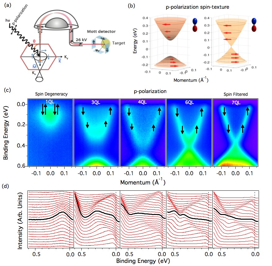
We used p-polarized light for our ARPES measurements. The photons approach the sample surface with angle of incident () 45 degree with the sample normal and our samples are aligned along momentum-space cut (Fig. 2a) for spin-ARPES measurements. The surface wavevector dependent spin polarization is obtained using a Mott-polarimeter (Fig. 2(a)), which measures two orthogonal spin components of a photoemitted electron Berntsen ; Hugo . In the polarimeter, a gold foil was used as a scattering source to generate an asymmetry of high energy photoelectrons into different divergent spin states (see Hugo ; Berntsen for details). Each orthogonal spin-polarization component is selected by the orientation of a scattering plane defined by the incident beam direction of the photoelectron on the gold foil and the orientation of two electron detectors mounted on each side of the foil. For this experiment, the detector configuration was set in a way that the two spin components correspond to the in-plane and out-of-plane directions of the (111) plane of the sample.
Thickness and wavevector dependent spin polarization
We present high-resolution spin-integrated ARPES data and corresponding energy distribution curves (EDCs) along the high symmetry line for 1QL, 3QL, 4QL, 6QL and 7QL Bi2Se3 films in Figs. 2(c) and 2(d). As long as the thickness of the film is comparable to the decay length of the surface states into the bulk, there is a spatial overlap between the top and bottom surface states resulting in an energy gap at the time-reversal invariant point ( point). As expected theoretically Linder ; HZLu , the energy gap decreases and eventually vanishes for sufficiently thick films, corresponding to the transition from a 2D gapped system (insulator) to a 3D gapless system (metal) QiKunXue ; Sakamoto . In particular, the gapless dispersion relation observed in the 7QL film from ARPES measurement indicates that this thickness is above the quantum tunneling limit. Based on experimental observations, we present an illustration of the spin configuration for 3QL (insulator) (see Supplementary Figures 2 and 3, and Supplementary Note 2) and 7QL (metal) ultrathin Bi2Se3 films in Fig. 2(b). It is important to note that a wide range of electronic structures have been reported in ultrathin TI films grown by MBE depending on the nature of the substrates used QiKunXue ; Sakamoto ; Tjernberg . Different substrates result in different potential jump from the substrate (the bottom surface of the ultra-thin film) to the vacuum (the top surface of the film). When the potential is large, the Dirac point energy of the bottom surface is offset with respect to that of the top surface. Such Dirac point energy offset is observed to cause sizeable Rashba-type splitting of surface states as reported in ultrathin Bi2Se3 films grown on double-layer-graphene-terminated 6H-SiC (0001) substrate QiKunXue and Bi-terminated Si(111)-(77) Tjernberg substrate by MBE, respectively. On the other hand, no observable Rashba-type splitting due to substrate potential is reported in the Bi2Se3 grown on Si(111)-Bi substrate (in Ref. Sakamoto ), -Al2O3 (sapphire) (0001) substrate (in Ref. QKXue ) and our current work GaAs(111)A.
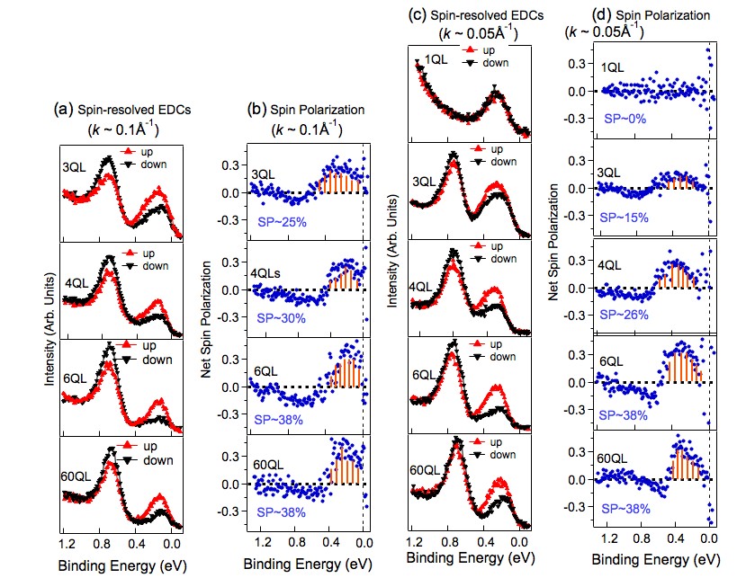
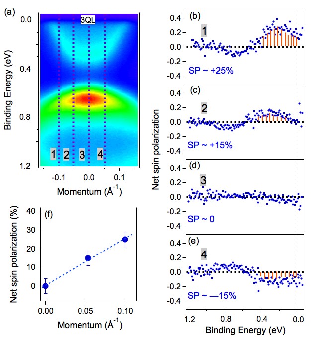
We investigate the degree of spin polarization of the films as a function of electron wavevector for films of various thickness. To illustrate the wavevector dependent spin polarization, 3QL film is chosen ( see Supplementary Figures 2 and 3, and Supplementary Note 2 for details). The SR-ARPES data for the wavevectors 0.05 Å-1 and 0.1 Å-1 are presented in Fig. 3. For each wavevector selected we present a spin-resolved energy distribution curve (EDC), which shows the relative intensity of photoelectrons with up and down spin polarizations (Figs. 3(a) and 3(c)). For each such plot we associate a net spin polarization with the surface state of a given wavevector (Figs. 3(b) and 3(d)) and for 3QL film about 25 and 15 are estimated at momenta 0.1 Å-1 and 0.05 Å-1, respectively. From these plots it is clearly observed that the net spin polarization decreases for smaller wavevectors (locations k 0.05 Å-1 in Fig. 3(d)). The decrease can be understood as the presence of a tunneling gap in the ultrathin limit that effectively prevents the partner-switching behavior expected in the gapless topological surface states system HZLu . The tunneling gap for ultrathin films can be seen in the data (Fig. 2(c)). The reduction of the spin polarization and the existence of a tunneling gap in the data suggest that the bottom surface’s right-handed contribution to the spin polarization must increase to effectively cancel the top surface’s left-handed helical spin texture upon approaching smaller momenta values near .
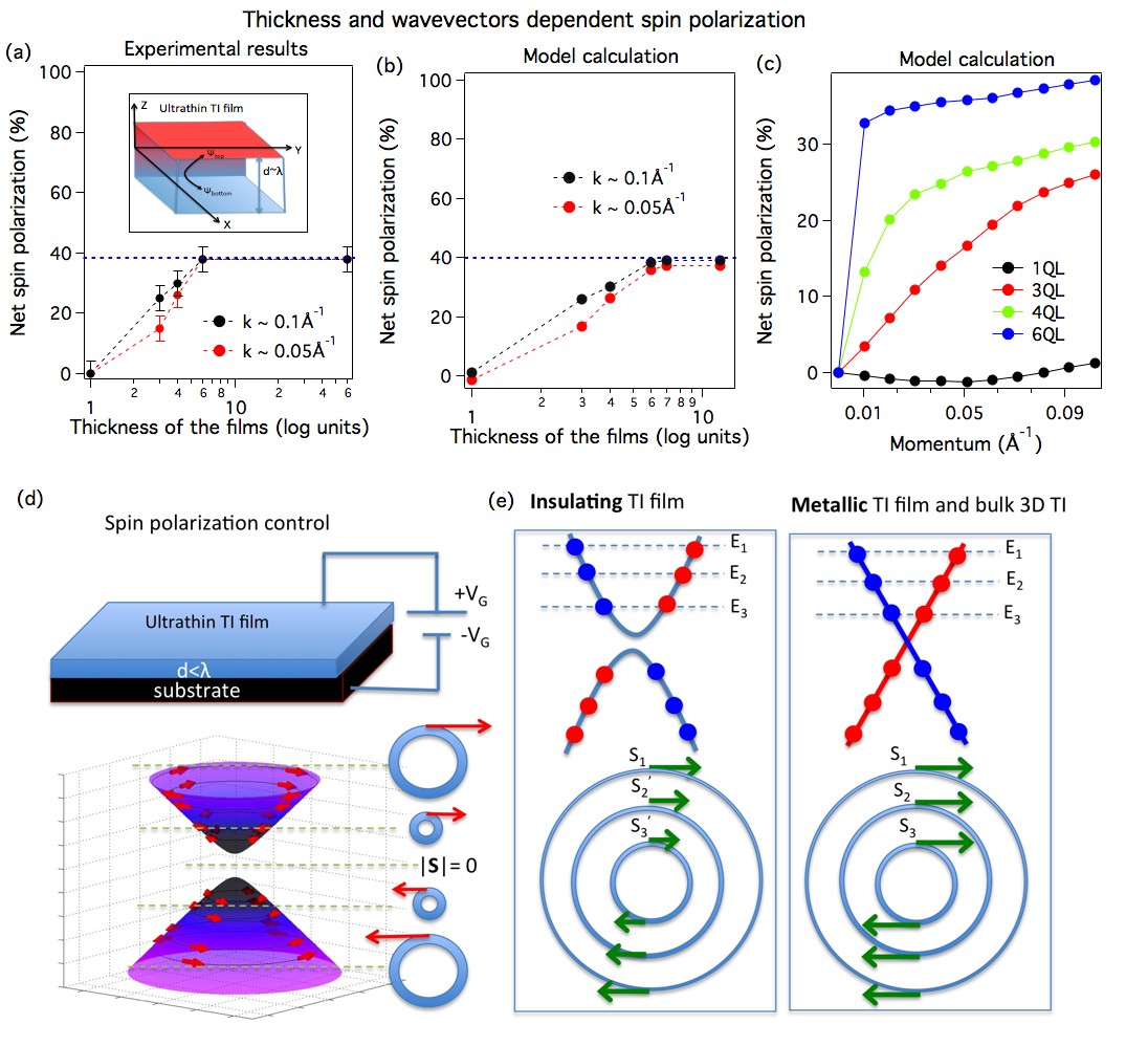
Fig. 3(a) shows the spin-resolved EDCs for 3QL, 4QL, 6QL and 60QL films while the corresponding net polarization is shown in Fig. 3(b) at = 0.1 Å-1. Analogous measurements are shown in Figs. 3(c) and 3(d) at = 0.05 Å-1 for 1QL, 3QL, 4QL, 6QL and 60QL films. For thinner films, such as 3QL, there is a naturally larger contribution from the bottom surface (due to tunneling between top and bottom surfaces). This leads to a larger variation in spin polarization as a function of wavevector. For thicker films, this tunneling contribution decreases and the surface spin polarization becomes more uniform with varying wavevector. For instance, in the 60QL film, no measurable change in spin polarization is observed for the variation in wavevector magnitude. Our data suggest that the magnitude of polarization tends to reach the bulk limit faster at larger wavevectors. Experimental results are summarized in Fig. 4(a). Data further suggest that the relative contribution from the top surface systematically increases with film thickness.
Model calculation
First-principles theoretical modeling of the spin polarization behavior in thin films is presented in Figs. 4(b) and 4(c). In the calculations, symmetric slabs are used to simulate the thickness of films. While a gapless spin-polarized Dirac cone is seen on the surface of a semi-infinite crystal of the topological insulator Bi2Se3, a gap is found to open at the Dirac point for thin films due to a finite tunneling amplitude between the two sides of the slab surface in our calculations. The tunneling amplitude increases as the thickness decreases, causing the gap to increase and spin polarization to decrease in the gap region. In the calculation we also consider the electron attenuation length () due to the scattering processes since only electrons near the surface are able to reach the top of the surface and escape into the vacuum as in the measurement condition. Indeed, the spin polarization obtained by ARPES reflects the spin-texture of the states associated with top surface rather than the bottom surface. The calculated spin expectation value for the electrons that can escape from the sample is ), where is the distance of an atom to the top surface, and the is the spin expectation value for each atom. The contribution from each atom is weighted by exp(), which reduces the contribution from the bottom layer. Figs. 4(b) and 4(c) show the calculated results with = 8Å, which agree excellently with our experimental observation (see Supplementary Methods for detailed related to calculations).
Discussion
It is important to note that the maximum spin polarization observed in the bulk limit is only about 40% (Fig. 4(c)) whereas the original ideal theoretical limit is that of nearly 100% without considering any specific material system Kane . In real TI materials, the strong spin-orbit interaction entangles the spin and orbital momenta of different atomic types, resulting in the reduction of spin polarization spin . Specifically, the low-energy states in Bi2Se3 arise from -orbitals of Bi (6) and Se (4), mostly levels of Bi and Se Matthew Nature physics BiSe ; SCZhang . The dominance of the orbitals in the topological surface states is further suggested by our circular dichroism (CD) measurements (see Supplementary Figure 4, Supplementary Note 2 and Supplementary Methods) . The spin-orbit coupling mixes spin and orbital angular momenta while preserving the total angular momentum Matthew Nature physics BiSe ; SCZhang . The hybridization of orbitals in Bi and Se together with the entanglement of their spins contribute to the reduction of net spin polarization in real materials. Moreover, under the experimental geometry used in our measurement with polarized light (which is most sensitive to orbitals and most reflective of initial groundstate of the wavefunction), the penetration depth of the ARPES experiment (3-5 atomic layers maximum), the experimental observation of spin polarization is well agreed with recent theoretical calculations Park ; Oliver .
Most importantly, our systematic spin-spectroscopy results suggest that ultrathin films can serve as the basis for making qualitatively new devices, not possible with much-studied conventional 3D bulk topological insulators, despite the reduction of the polarization magnitude. The energy-momentum space spin texture revealed in our study provides critical knowledge to design and interpret devices based on ultrathin films. For spintronics applications, our results suggest that ultrathin topological insulator films can be used to fabricate new types of nano-devices due to the novel spin configurations and their systematic modulations possible in the ultrathin limit. One such potential application implied by our spectroscopic results is that of a polarization current switch. Spin spectroscopic results suggest that it should be possible to control the polarization magnitude by varying a gate voltage (Figs. 4(d) and 4(e)) across a high quality insulating thin film (see supplementary Figure 5 and Supplementary Note 3). Such electrostatic gating would be similar to the in-situ chemical gating by K-deposition and NO2 adsorption shown in Supplementary Figures 6 and 7, where the surface state structure does not change appreciably, while the Fermi energy is moved from regions of high polarization to low polarization (see Supplementary Note 3). This effect, which cannot be readily realized in the highly-polarized states of conventional 3D bulk TIs, allows ultrathin TI films to serve as the basis for functional nano-devices which can encode electrical signals in varying spin polarization magnitude or forms the physical basis for a spin switch, among many other new application possibilities suggested by our observations of the fundamental spin modulation behavior in ultrathin films.
Methods
Sample growth and transport measurements
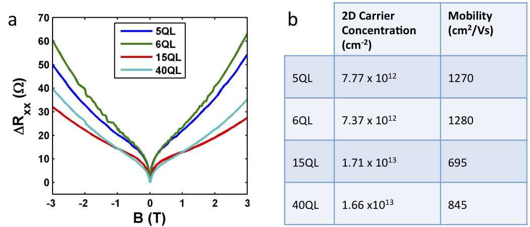
Ultrathin Bi2Se3 films used for this study were synthesized by molecular beam epitaxy (MBE) on a GaAs(111)A substrate with a ZnSe buffer layer. Details of sample preparation are described elsewhere Suyang ; DZhang . To protect the surface from oxidation, a thick Se capping layer was deposited on the Bi2Se3 thin film immediately after growth. To achieve the clean Bi2Se3 surface required for photoemission measurements, thin films were heated up inside the ARPES chamber to 250 ∘C under vacuum better than 1 10-9 torr to remove the Se capping layer on top of ultrathin Bi2Se3. Hall bars fabricated from the Se capped samples had carrier concentrations in the 1 to 2 1019cm-3 range. Transport measurements were carried out on Hall bars of the 5 and 6QL thick films with the Se capping layer in place by standard photolithography and dry etching and were measured at 4.2 K.
High-resolution ARPES measurements
High-resolution spin-integrated angle-resolved photoemission spectroscopy (ARPES) measurements were performed with 29-64 eV photon energy on beamlines 10.0.1 and 12.0.1 at the Advanced Light Source (ALS) in Lawrence Berkeley National Laboratory (LBNL). Both endstations were equipped with a Scienta hemispherical electron analyser (see VG Scienta manufacturer website, (http://www.vgscienta.com/), for instrument specifications). The typical energy and momentum resolutions were 15 meV and 1% of the surface Brillouin zone, respectively for spin-integrated measurements.
Spin-resolved ARPES measurements
Spin-resolved ARPES measurements were performed at the UE112-PGM1 beamline at Bessy II in Berlin, Germany, and the I3 beamline at Maxlab in Lund, Sweden, using classical Mott detectors and photon energies 55 to 60 eV and 8 to 20 eV, respectively. The typical energy and momentum resolutions were 100 meV and 3% of the surface Brillouin zone for spin-resolved measurements. All the SR-spectra presented are measured in BESSY II unless it is specified.
Theoretical calculations
The first-principles calculations for spin polarizations of ultrathin films are based on the generalized gradient approximation (GGA) Perdew using the full-potential projected augmented wave method Blochl ; Bloch_1 as implemented in the VASP package Kress . The 1QL, 3QL, 4QL, 6QL, 7QL, and 12QL slab models with a vacuum thickness larger than 10 are used in this work. The electronic structure calculations were performed over 11111 Monkhorst-Pack k-mesh with the spin-orbit coupling included self-consistently.
References
- (1) Moore, J. E. The birth of topological insulators. Nature , 194-198 (2010).
- (2) Hasan, M. Z. & Kane, C. L. Colloquium: topological insulators. Rev. Mod. Phys. , 3045-3067 (2010).
- (3) Qi, X-L. & Zhang, S-C. Topological insulators and superconductors. Rev. Mod. Phys. , 1057-1110 (2011).
- (4) Fu, L. & Kane, C. L. Topological insulators with inversion symmetry. Phys. Rev. B , 045302 (2007).
- (5) Hsieh, D. et al. A topological Dirac insulator in a quantum spin Hall phase. Nature , 970-974 (2008).
- (6) Xia, Y. et al. Observation of a large-gap topological-insulator class with a single Dirac cone on the surface. Nature Phys. , 398-402 (2009).
- (7) Chen, Y.-L. et al. Massive Dirac Fermion on the surface of a magnetically doped topological insulator. Science , 659-662 (2010).
- (8) Xu, S.-Y. et al. Observation of a topological crystalline insulator phase and topological phase transition in Pb1-xSnxTe. Nature Comm. , 1192 (2012).
- (9) Neupane, M. et al. Surface electronic structure of the topological Kondo-insulator candidate correlated electron system SmB6. Nature Comm. , 2991 (2013).
- (10) Zhang, Y. et al. Crossover of the three-dimensional topological insulator Bi2Se3 to the two-dimensional limit. Nature Phys. , 584-588 (2010).
- (11) Sakamoto, Y. et al. Spectroscopic evidence of a topological quantum phase transition in ultrathin Bi2Se3 films. Phys. Rev. B , 165432 (2010).
- (12) Zhang, H. et al. Topological insulators in Bi2Se3, Bi2Te3 and Sb2Te3 with a single Dirac cone on the surface. Nature Phys. , 438-442 (2009).
- (13) Hsieh, D. et al. A tunable topological insulator in the spin helical Dirac transport regime. Nature , 27 (2009).
- (14) Liu, C.-X. et al. Oscillatory crossover from two-dimensional to three-dimensional topological insulators. Phys. Rev. B , 041307(R) (2010).
- (15) Jiang, Y. et al. Landau Quantization and the Thickness Limit of Topological Insulator Thin Films of Sb2Te3. Phys. Rev. Lett. 108, 016401 (2012).
- (16) Taskin, A. A. et al. Manifestation of topological protection in transport properties of epitaxial Bi2Se3 thin films. Phys. Rev. Lett. 109, 066803 (2012).
- (17) Neupane, M. et al. Topological surface states and Dirac point tuning in ternary topological insulators. Phys. Rev. B , 235406 (2012).
- (18) Berntsen, M. H. et al. Direct observation of decoupled Dirac states at the interface between topological and normal insulators. Phys. Rev. B , 195132 (2013).
- (19) Chang, C.-Z. et al. Growth of topological insulator Bi2Se3 on insulating substrate. Spin , 21-25 (2011).
- (20) Garate, I. & Franz, M. Inverse spin-galvanic effect in the interface between a topological insulator and a ferromagnet. Phys. Rev. Lett. 104, 146802 (2010).
- (21) Qi, X.-L. et al. Inducing a magnetic monopole with topological surface states. Science , 1184-1187 (2009).
- (22) Essin, A., Moore, J. E. & Vanderbilt, D. Magnetoelectric polarizability and axion electrodynamics in crystalline insulators. Phys. Rev. Lett. , 146805 (2009).
- (23) Yu, R. et al. Quantized anomalous Hall effect in magnetic topological insulators. Science , 61-64 (2010).
- (24) Linder, J. et al. Unconventional superconductivity on a topological insulator. Phys. Rev. Lett. , 067001 (2010).
- (25) Fu, L. & Kane, C. L. Probing neutral Majorana fermion edge modes with charge transport. Phys. Rev. Lett. , 216403 (2009).
- (26) Linder, J., Yokoyama, T. & Sudbo, A. Anomalous finite size effects on surface states in the topological insulator Bi2Se3. Phys. Rev. B , 205401 (2009).
- (27) Lu, H.-Z. et al. Massive Dirac fermions and spin physics in an ultrathin film of topological insulator. Phys. Rev. B , 115407 (2010).
- (28) Lu, H.-Z. et al. Competition between weak localization and antilocalization in topological surface states. Phys. Rev. Lett. 107, 076801 (2011).
- (29) Berntsen, M. H. A spin- and angle-resolving photoelectron spectrometer. Rev. Sci. Instrum , 035104 (2010).
- (30) Dil, J. H. Spin and angle resolved photoemission on non-magnetic low-dimensional systems. Phys. Condens. Matter , 403001 (2009).
- (31) Kane, C. L. & Mele, E. J. Z2 Topological order and the quantum spin Hall effect. Phys. Rev. Lett. 95, 146802 (2005).
- (32) Yazyev, O. V., Moore, J. E. & Louie, S. G. Spin polarization and transport of surface states in the topological Insulators Bi2Se3 and Bi2Te3 from first principles. Phys. Rev. Lett. 105, 266806 (2010).
- (33) Zhu, -H. Z. et al. Layer-by-layer entangled spin-orbital texture of the topological surface state in Bi2Se3. Phys. Rev. Lett. 110, 216401 (2013).
- (34) Park, S. R. et al. Chiral orbital-angular momentum in the surface states of Bi2Se3. Phys. Rev. Lett. , 046805 (2012).
- (35) Sánchez-Barriga, J. et al. Photoemission of Bi2Se3 with circularly polarized light: probe of spin polarization or means for spin manipulation? Phys. Rev. X , 011046 (2014).
- (36) Xu, S.-Y. et al. Hedgehog spin texture and Berry s phase tuning in a magnetic topological insulator. Nature Phys. , 616-622 (2012).
- (37) Zhang, D. et al. Interplay between ferromagnetism, surface states, and quantum corrections in a magnetically doped topological insulator. Phys. Rev. B 86, 205127 (2012).
- (38) Perdew, J. P., Burke, K. & Ernzerhof, M. Generalized gradient approximation made simple. Phys. Rev. Lett. 77, 3865 (1996).
- (39) Blchl, P. E. Projector augmented-wave method. Phys. Rev. B 50, 17953 (1994).
- (40) Kresse, G. & Joubert, J. From ultrasoft pseudopotentials to the projector augmented-wave method. Phys. Rev. B 59, 1758 (1999).
- (41) Kress, G. & Hafner, J. Ab initio molecular dynamics for open-shell transition metals. Phys. Rev. B 48, 13115 (1993).
Acknowledgements. Sample growth and ARPES characterization are supported by US DARPA (N66001-11-1-4110). The work at Princeton University and Princeton-led synchrotron X-ray-based measurements and the related theory at Northeastern University are supported by the Office of Basic Energy Science, US Department of Energy (grants DE-FG-02-05ER462000, AC03-76SF00098 and DE-FG02-07ER46352). M.Z.H. acknowledges visiting-scientist support from Lawrence Berkeley National Laboratory and additional support from the A. P. Sloan Foundation. The spin-resolved and spin-integrated photoemission measurements using synchrotron X-ray facilities are supported by the Swedish Research Council, the Knut and Alice Wallenberg Foundation, the German Federal Ministry of Education and Research, and the Basic Energy Sciences of the US Department of Energy. Theoretical computations are supported by the US Department of Energy (DE-FG02-07ER46352 and AC03-76SF00098) as well as the National Science Council and Academia Sinica in Taiwan, and benefited from the allocation of supercomputer time at NERSC and Northeastern University’s Advanced Scientific Computation Center. We also thank S-K. Mo and A. Fedorov for beamline assistance on spin-integrated photoemission measurements (supported by DE-FG02-05ER46200) at Lawrence Berkeley National Laboratory (The synchrotron facility is supported by the US DOE).
Author contributions
M.N., J.S.-B, and S.-Y.X. performed the experiments with assistance from N.A., I.B., C.L., G.B., D.M., A.V., O.R., M.L., T.B. and M.Z.H.; A.R, D.M.Z and N. S. provided thin film MBE samples and performed sample characterization; M. N. and M. Z. H performed data analysis, figure planning and draft preparation.
T.R.C., H.T.J., S.B., H.L., and A.B. carried out calculations; M.Z.H. was responsible for the conception and the overall direction, planning and integration among different research units.
Additional information
Supplementary Information accompanies this paper is available at http://www.nature.com/naturecommunications.
Competing financial interests: The authors declare no competing financial interests.
Correspondence and requests for materials should be addressed to
M.Z.H. (Email: mzhasan@princeton.edu).
Supplementary Information:
Observation of Quantum-Tunneling Modulated Spin Texture in Ultrathin Topological Insulator Bi2Se3 Films
This files includes:
| Supplementary Figures |
| Supplementary Notes |
| Supplementary Methods |
| Supplementary References |
.1 Supplementary Figures


.2 Supplementary Note 1
Transport measurements of thin films
We performed systematic magnetotransport measurements for TI thin films with various thicknesses. Films were patterned into Hall bars using photolithography and measured using a standard AC lock-in at liquid helium temperatures. The change in magnetoresisistance for different Bi2Se3 film thicknesses is shown in Supplementary Figure 1. An increasing weak-antilocalization component of the total magnetoresisistance is seen as the films become thinner. This correction is described by the Hikami-Larkin-Nagaoka equation and is due to conduction through the surface states. Fits yield values of alpha between -0.5 and -1 and phase breaking lengths of approximately 100 to 200 nm. The 2D carrier concentration was calculated from linear fits to the Hall voltage. It rises for thicker films but does not scale linearly the thickness, indicating a large component of the carriers are in the 2D surface state. The results are consistent with published results [1, 2].
.3 Supplementary Note 2
Spin polarization measurements of ultrathin 3QL film
We investigate the degree of spin polarization of the films as a function of electron wavevector. Based on these data presented in Supplementary Figure 2, it is evident that the spin signal is dominated by the contribution from the top surface since it reveals a characteristic left-handed helical spin-texture (see the spin polarization at locations # 2,4) signaling topological order [3]. For smaller wavevectors, net spin polarization is seen to decrease (locations #2,4 in Supplementary Figure 2(a)). The decrease can be understood as the presence of a tunneling gap in the ultrathin limit that effectively prevents the partner-switching behavior expected in the gapless topological surface states system [4]. The tunneling gap for ultrathin films can be seen in the data (Supplementary Figure 2(a)). The reduction of spin polarization and the existence of a tunneling gap in the data suggest that the bottom surface contribution of spin polarization must increase to effectively cancel the left-handed helical spin upon approaching smaller momenta values toward . Similarly at the time-reversal invariant point (point #3 in Supplementary Figure 2(a)), namely at , a nearly ideal cancellation between top and bottom surfaces happens resulting in zero net spin polarization, which is consistent with the time-reversal symmetry of the electronic structure of the films [4].
Absence of the out-of-plane spin component in ultrathin TI film
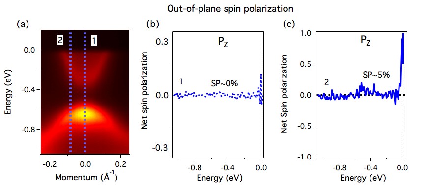
Here we present an out-of-plane spin measurement of a 3QL ultrathin TI film performed at the I3 beamline at Maxlab [5]. Supplementary Figure 3(a) shows the spin-integrated ARPES data with blue dashed lines and integer numbers indicating the momentum positions for the spin-resolved measurements. The net spin polarization is shown in Supplementary Figure 3(b) and 3(c) for momenta positions mark as 1 and 2, respectively. Our spin polarization result in Supplementary Figure 3(b) indicates that the out-of-plane spin polarization is zero at the time-reversal invariant point (), which is in sharp contrast to magnetically doped topological insulator [6]. The absence of an out-of-plane spin component at implies that the origin of gap is purely quantum tunneling between the top and bottom surfaces of the ultrathin TI. Similarly, a small out-of-plane spin component is observed at momentum position 2 , which is within the experimental resolution. The negligible out-of-plane component of spin polarization at momentum position away from the time-reversal symmetry breaking point (Supplementary Figure 3(c)) indicates near absence of the Fermi surface warping on the 3QL film Dirac cone.
CD-ARPES measurements
The experimental geometry used for the circular dichroism (CD) measurements is present in Supplementary Figure 4(a). The sample surface is parallel to the XY plane and circularly polarized photons (spiral arrow) propagate in the XZ plane at an angle () of 50∘ to the sample surface normal. The ARPES dispersion maps of surface states measured using right circularly polarized (RCP) light and left circularly polarized (LCP) light for bulk Bi2Se3 are shown in Supplementary Figure 4(b). A clear surface state CD response on the photoelectron signal from the upper Dirac cone is observed where the +k Dirac branch shows stronger response for RCP light and the -k Dirac branch shows stronger response for LCP light (Supplementary Figure 4(b)). The magnitude of the CD response signal defined as =()/() is observed to be about 30% for incident photons with an energy of 19 eV in Bi2Se3 for electrons with binding energy of about 100meV, well below the chemical potential. This CD behavior is qualitatively consistent with previous work [7, 8]. Even though the ppolarized light probes both in-plane (, ) and out-of plane () orbitals revealing groundstate of the topological states, the topological surface states has dominant orbital character (up to 80%) [9, 10]. Based on our experimental geometry and the light polarization, the observation of strong CD response in bulk Bi2Se3 is likely coming from the orbitals of Bi and Se.
.4 Supplementary Note 3
Chemical potential tuning in ultrathin TI films
It is important to note that a wide range of electronic structures have been reported in ultrathin TI films grown by MBE depending on the nature of the substrates used [11-13]. Different substrates result in different potential gradient from the substrate (the bottom surface of the ultra-thin film) to the vacuum (the top surface of the film). When the potential is large, the Dirac point energy of the bottom surface is offset with respect to that of the top surface. Such Dirac point energy offset is observed to cause sizable Rashba-type splitting of surface states as reported in ultrathin Bi2Se3 films grown on double-layer-graphene-terminated 6H-SiC (0001) substrate [11] and Bi-terminated Si(111)-(77) [13] substrate by MBE, respectively. On the other hand, no observable Rashba-type splitting due to substrate potential is reported in the Bi2Se3 grown on Si(111)-Bi substrate (in ref [12]).
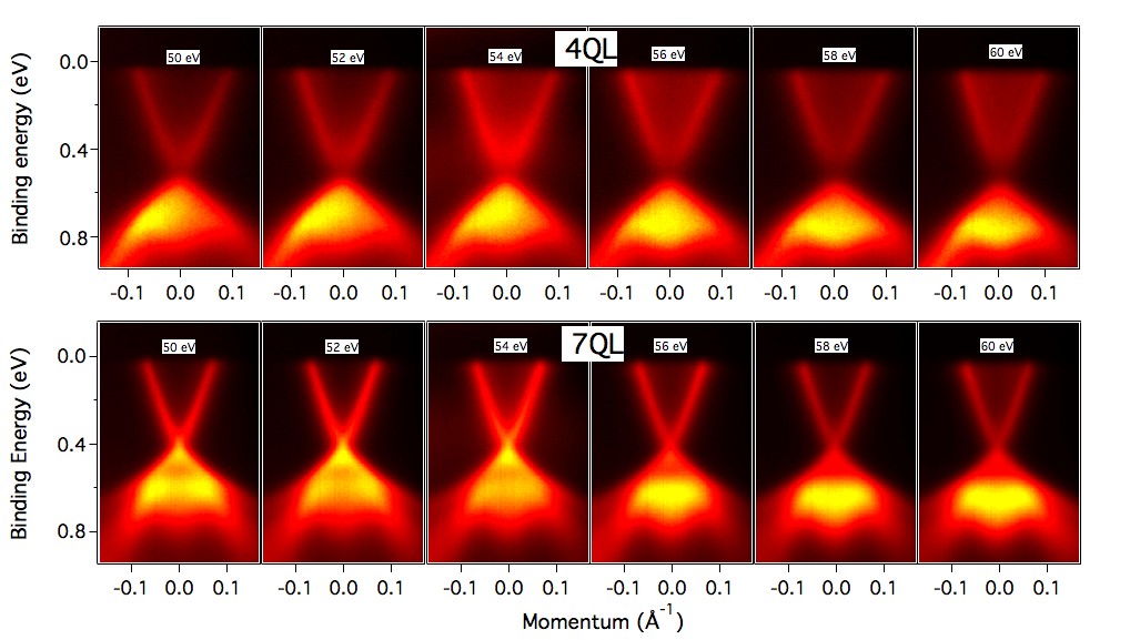
The photon energy dependent ARPES spectra for 4QL and 7QL films of Bi2Se3 are presented in Supplementary Figure 5. Nearly parabolic electronic band structure is observed in the binding energy of 500 meV for all photon energies with no observable additional features such as Rashba-like splitting in the 4QL film. Similarly for 7QL Bi2Se3 film which is just above the quantum tunneling limit, the Dirac like surface states do not disperse with varying photon energy. These photon energy dependent studies suggest that our GaAs(111)A substrate is similar to Si(111)-Bi substrate in ref [12], which implies nearly absence of the substrate-induced potential difference between the two surfaces. Nonetheless, we emphasize that for possible device applications it is essential to understand how the substrate-induced potential modifies the surface state dispersion relation at the interface between the substrate and the TI.
As discussed in the main text, our systematic results suggest that by varying the gate voltage, the spin polarization can be tuned to zero. This effect, which cannot be readily achieved using the highly-polarized surface states of bulk TIs, allows ultrathin film TIs to serve as the basis for a spintronics device which switches between a spin-polarized and non-polarized state depending on the gate voltage. This phenomena emphasizes the importance of understanding how spin configuration in topological materials is coupled to effects such as quantum tunneling.
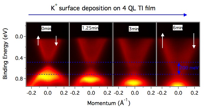
Here we demonstrate an example of surface gating by in situ surface chemical treatments such as surface deposition. Supplementary Figures 6 and 7 present the energy dispersion, measured by ARPES, along the momentum cut during potassium deposition and NO2 adsorption on a 4QL and 3QL ultrathin Bi2Se3 film, respectively. The potassium deposition surface treatment acts to dope the surface with electrons, raising the surface chemical potential by nearly 200 meV in 4QL film. This drives the system to a state of high surface spin polarization magnitude. On the other hand, NO2 adsorption moves the chemical potential to in-gap region, lowering the surface chemical potential by nearly 300 meV in 3QL film.
Electrostatic gating with a top or back gate wouldn’t be significantly different than the in-situ chemical doping as shown in Supplementary Figures 6 and 7, where the surface state structure didn’t change appreciably, while the Fermi energy is moved from regions of high polarization to low polarization. However, if there was an appreciable change in the coupling between the two surfaces this could be overcome by simultaneously gating the top and back surfaces to move the potential of both surfaces by the same amount as shown in ref [14]. Regardless of the technical details of proposed thin film devices, the energy-momentum space spin texture revealed in our study provides a critical knowledge to design and interpret the functional devices based on ultrathin films.
Furthermore, it is important to note that successive deposition of potassium on the surface of ultrathin Bi2Se3 film makes the ARPES spectrum broader. In spite of the broadened spectrum due to K+ ion coverage on the surface, it still can be observed that the gap at the Dirac point becomes smaller. While it is reasonable to assume that the electrons brought by potassium go into the film relatively homogeneously in axis, K+ ions stay on the surface and thus act as an effective gating that changes the potential difference between the top and the bottom surfaces. Similar broadening of the spectra also happened to be observed during NO2 adsorption.
.5 Supplementary Methods
Surface deposition: Potassium deposition was performed at beamline 12.0.1 of the ALS from a SAES getter source (SAES Getters USA, Inc.), which was thoroughly degassed before the experiment. Pressure in the experimental chamber stayed below torr during deposition. The deposition rate (/sec) was monitored using a commercial quartz thickness monitor (Leybold Inficon Inc., Model XTM/2). The deposition amount (thickness) was obtained by multiplying the deposition rate by the elapsed time.
Adsorption of NO2 molecules on surface of ultrathin 3QL Bi2Se3 film was achieved via controlled exposures to NO2 gas (Matheson, 99.5) at beamline 12.0.1 of the ALS. The adsorption effects were studied under static flow mode by exposing the clean sample surface to the gas for a certain time at the pressure of torr, ARPES spectra were measured after the chamber was pumped down to the base pressure. Spectra of the NO2 adsorbed surfaces were taken within minutes of opening the photon shutter to minimize potential photon induced charge transfer and desorption effects.
CD-ARPES measurement: For CD-ARPES measurements, single crystalline samples of topological insulators were grown using the Bridgman method, which is detailed elsewhere [15]. ARPES measurements for the low energy electronic structure were performed at the Synchrotron Radiation Center (SRC), Wisconsin, equipped with high efficiency VG-Scienta SES2002 electron analyzer. The polarization purity is better than 99% for horizontal polarization (HP) and better than 80% for RCP and LCP. Samples were cleaved in situ and measured at 20 K in a vacuum better than 1 10-10 torr. Energy and momentum resolution were better than 15 meV and 1% of the surface Brillouin zone (BZ), respectively.
Theoretical calculation methods: Theoretical calculations presented in the main text are based on the generalized gradient approximation (GGA) [16] using the full-potential projected augmented wave method [17, 18] as implemented in the VASP package [19]. We use 1QL, 3QL, 4QL, 6QL, 7QL, and 12QL slab models with a vacuum thickness larger than . The electronic structure calculations were performed over a Monkhorst-Pack -mesh with the spin-orbit coupling included self-consistently.
In order to calculate the spin polarization, we consider the spin expectation value , where = atomic layer index, = momentum vector, = orbital index, = Pauli matrix, and = x, y, z. To simplify the calculation, (1) we choose momentum vector k along high symmetry direction . Due to the mirror symmetry, we have, and (2) only focus near Dirac point where the hexagonal warping effect is small, so can be neglected. Therefore, only y components survive. We ignore subindex y to simplify notation, . In the calculation we also consider the electron attenuation length () due to the scattering processes since only electrons near the surface are able to reach the top of the surface and escape into the vacuum as in the measurement condition. Indeed, the spin polarization obtained by ARPES reflects the spin-texture of the states associated with top surface rather than the bottom surface. The calculated spin polarization for the electrons that can escape from the sample is with proper normalization, where is the distance of an atom to the top surface, and the is the spin expectation value for each atom and k point. The contribution from each atom is weighted by , which reduces the contribution from the bottom layer. Figs. 4(b) and 4(c) show the calculated results with .
.6 Supplementary References
| Richardella, A. et al. Coherent heteroepitaxy of Bi2Se3 on GaAs (111)B. | |
| Appl. Phys. Lett. , 262104 (2010). | |
| Taskin, A. A. et al. Manifestation of topological protection in transport | |
| properties of epitaxial Bi2Se3 thin films. Phys. Rev. Lett. , 066803 (2012). | |
| Hsieh, D. et al. A tunable topological insulator in the spin helical Dirac transport | |
| regime. Nature , 27 (2009). | |
| Lu, H.-Z. et al. Massive Dirac fermions and spin physics in an ultrathin film of | |
| topological insulator. Phys. Rev. B , 115407 (2010). | |
| Berntsen, M. H. A spin- and angle-resolving photoelectron spectrometer. | |
| Rev. Sci. Instrum , 035104 (2010). | |
| Xu, S.-Y. et al. Hedgehog spin texture and Berry s phase tuning in a magnetic | |
| topological insulator. Nature Phys. , 616-622 (2012). | |
| Neupane, M. et al. Oscillatory surface dichroism of the insulating topological | |
| insulator Bi2Te2Se. Phys. Rev. B , 165129 (2013). | |
| Wang, Y. and Gedik, N. Circular dichroism in angle-resolved photoemission | |
| spectroscopy of topological insulator. Phys. Status Solidi RRL , 64 (2013). | |
| Zhu, -H. Z. et al. Layer-by-layer entangled spin-orbital texture of the | |
| topological surface state in Bi2Se3. Phys. Rev. Lett. 110, 216401 (2013). | |
| Park, S. R. et al. Chiral orbital-angular momentum in the surface states | |
| of Bi2Se3. Phys. Rev. Lett. , 046805 (2012). | |
| Zhang, Y. et al. Crossover of the three-dimensional topological insulator | |
| Bi2Se3 to the two-dimensional limit. Nature Phys. , 584-588 (2010). | |
| Sakamoto, Y. et al. Spectroscopic evidence of a topological quantum phase | |
| transition in ultrathin Bi2Se3 films. Phys. Rev. B , 165432 (2010). | |
| Berntsen, M. H. et al. Direct observation of decoupled Dirac states at the interface | |
| between topological and normal insulators. Phys. Rev. B , 195132 (2013). | |
| Liu, H. & Ye, P. D. et al., Atomic-layer-deposited Al2O3 on Bi2Te3 for topological | |
| insulator field-effect transistors. App. Phys. Lett. , 052108 (2011). | |
| Jia, S. et al., Defects and high bulk resistivities in the Bi-rich tetradymite | |
| topological insulator Bi2+xTe2-xSe. Phys. Rev. B , 165119 (2012). |
| Perdew, J. P., Burke, K. & Ernzerhof, M. Generalized gradient approximation | |
| made simple. Phys. Rev. Lett. 77, 3865 (1996). | |
| Blchl, P. E. Projector augmented-wave method. Phys. Rev. B 50, 17953 (1994). | |
| G. Kresse, G. & Joubert, J. From ultrasoft pseudopotentials to the projector | |
| augmented-wave method. Phys. Rev. B 59, 1758 (1999). | |
| Kress, G. & Hafner, J. Ab initio molecular dynamics for open-shell transition | |
| metals. Phys. Rev. B 48, 13115 (1993). |
Correspondence and requests for materials should be addressed to M.Z.H. (Email: mzhasan@princeton.edu).