IR,NMR,UV
Silicene as a new ultrafast DNA sequencing device
Abstract
Silicene, a hexagonal buckled 2-D allotrope of silicon, shows potential as a platform for numerous new applications, including bio-sensing. We have used density functional theory, incorporating corrections to account for van der Waals interaction, to investigate the adsorption of individual nucleobases on silicene. Our study sheds light on the stability of this novel nano-bio system, its electronic properties and the pronounced effects on the transverse electronic transport, i.e., changes in the transmission and the conductance caused by adsorption of each nucleobase, explored by us through the non-equilibrium Green’s function method. Intriguingly, despite the relatively weak interaction between nucleobases and silicene, significant changes in the transmittance at zero bias are predicted by us, in particular for the two nucleobases cytosine and guanine. Our findings suggest that silicene could be utilized as an integrated-circuit biosensor as part of a lab-on-a-chip device for DNA analysis.
keywords:
American Chemical Society, LaTeXIt has long been known that, under standard conditions, graphite is the most stable form of carbon while silicon takes on the diamond cubic crystal structure. This natural circumstance is a direct reflection of the greater stability of the hybridization in C and of the hybridization in Si. Nonetheless, it was theoretically predicted 1, 2, 3, 4 and subsequently experimentally confirmed 5, 6, 7, 8, 9, 10, 11, that a 2-D honeycomb lattice like graphene can also be formed by Si, named silicene. Despite some structural similarities of silicene with graphene, the two differ in a couple of crucial aspects: firstly, the most stable structure of silicene is not planar, but buckled. This feature was described already in its original theoretical prediction 1, 4 and also observed in experiments 7, 10, 11. Secondly, the method to obtain silicene is rather different from that used originally for graphene 12, in that for silicene one cannot apply the exfoliation method since this allotrope of silicon cannot freely exist in nature. Instead, the prevalent method to synthesize silicene is to deposit Si atoms on a substrate in the form of a metal surface.
In the present work, we investigate whether silicene could be used for third-generation DNA sequencing 13, 14, 15, 16, 17, 18, 19. Graphene has been extensively studied with this application in mind 20, 21, 22, 23, 24, 25, 26, 27, 28, 29, 30, 31, 32, 33, 34, 35, 36, 37, 38, 39, 40, 41, 42, 43, 44, 45, 46, 47. Silicene represents an interesting alternative and might even offer an advantage here over graphene in terms of integrability with existing silicon-based microchip technology. To evaluate its capability for distinguishing the four different nucleobase types of DNA electronically, we investigated the stability, electronic structures and transport properties of silicene with each nucleobase adsorbed on top of silicene. This approach resembles most closely that investigated by the group of K. S. Kim for graphene nanoribbons 25, 26. Our results reveal that, although the electronic structure is not drastically changed due to the relatively weak interaction, it might be possible to detect the nucleobase type by analyzing subtle changes in the transport properties of the systems.

1 Pristine Silicene
In order to establish the reliability of our computational methods to accurately describe pristine silicene itself, we first carried out a number of benchmark tests concerning the structural and electronic properties of silicene. Figure 1 shows the fully relaxed supercell for flat and buckled structures in which represents the vertical distortion of the atomic positions from a perfectly planar geometry. The flat structure is found to be metastable in the sense that a small out-of-plane displacement of the atoms would lead to the sheet becoming buckled upon relaxation. Both the hexagonal and parallelepiped unit cells with two and four atoms, respectively, were considered by us (Figure 1). The relaxed lattice constant, Si-Si distance, and resulting vertical distortion are listed in Table 1, calculated with the exchange-correlation potential GGA (PBE) and with GGA including van der Waals (vdW) corrections. Our results for the Si-Si distance ( Å) are in excellent agreement with experimental results 10 ( Å) and with recent theoretical predictions4 ( Å). For the proper description of pristine silicene, it is of rather little difference whether vdW corrections are added to GGA or not. However, since a major goal of our present work is to study the physisorption of DNA nucleobases on silicene, a process in which vdW interactions may be crucial, the conclusion from our benchmark results in Table 1 is that GGA+vdW does indeed yield accurate results for pristine silicene.
| GGA | GGA+vdW | |||||
|---|---|---|---|---|---|---|
| structure | ||||||
| planar | ||||||
| buckled | ||||||
We furthermore investigated the energetic properties of pristine silicene, as summarized in Figure 2a. It can be seen that the buckled structure is approximately 0.05 eV/atom more stable than the planar one, in agreement with theoretical predictions4 and the experimental10, 11 findings that silicene exists in a buckled configuration. Calculated band structures for the planar and buckled structures are compared in Figure 2b. One can note the similarities with the band structure of graphene, inasmuch as we observe the same crossing of the and bands at and points in the Brillouin zone. The main difference between the electronic band structures of the planar and buckled geometries is a varying shift in energy of the respective bands, with the magnitude of the shift smoothly changing as we move through reciprocal space.
The calculated transmittance shown in Figure 2c and 2d considers transport in directions perpendicular to zigzag (c) and armchair (d) rows. As we can see, transport perpendicular to the zigzag rows exhibits a gap in the transmittance at , while transport perpendicular to the armchair rows possess finite normalized transmittance for all energies. This difference is solely due to the computational necessity of using a finite grid of -points for Brillouin zone sampling. If an infinitely dense grid -points could be considered, the electronic transmission curves for both directions would be indistinguishable and the discrete steps would take on an essentially smooth linear shape as is common for Dirac materials.

2 Equilibrium Geometries
Having established the basic structural and electronic properties of pristine silicene and their accurate description through the computational methods chosen by us in the present study, we now turn our attention to the main focus of this paper, namely the physisorption of DNA nucleobases on silicene and the consequential effects on the electronic conductance properties of this nano-bio hybrid system.
The fully relaxed equilibrium geometries of the four DNA nucleobases adenine, cytosine, guanine, and thymine (abbreviated as A, C, G, and T in the following) physisorbed on silicene are shown in the left panel of Figure 3. We first note the larger size of the underlying hexagons formed by the silicon atoms compared to the smaller six- and five-membered rings formed by carbon and nitrogen atoms in the nucleobases. This size mismatch is an important difference to similar physisorption processes of DNA nucleobases on graphene and boron nitride studied in the past 48, 49, 50.

One feature discernible from the side view of Figure 3 is that cytosine and guanine have their single oxygen atom located directly above a silicon atom. For thymine with its two oxygen atoms, no such alignment is observed (and for geometrical reasons, it is actually impossible to align both oxygen atoms simultaneously on top of the underlying silicon atoms without inducing drastic deformations in the bond angles or bond lengths of thymine). In terms of the equilibrium distance between nucleobases and silicene, we can distinguish two categories: one category (A and T) in which the closest atomic distance between the two entities is a (non-covalent) Si–H connection with a distance of about 3 Å and a second category (C and G) in which the closest distance is given by a Si–O connection amounting merely to around 2 Å. These results are quantitatively summarized in Table 2. The correlation between equilibrium distance and binding energy is discussed further below.
| nucleobase | closest atoms | distance Si-base | binding energy |
|---|---|---|---|
| A | Si-H | ||
| C | Si-O | ||
| G | Si-O | ||
| T | Si-H |
3 STM Images
In the right panel of Figure 3 we show through a series of simulated images how the four different nucleobases would appear in a scanning tunneling microscope (STM). To calculate the images, we apply the Tersoff-Hamann 52 approach, in which the electronic state of the STM tip is modeled by an -orbital and the assumption is made that the sample wave-functions near the tip exhibit only small variations. The resulting tunneling current (or rather differential conductance ) is proportional to local density of states (LDOS) or partial density of charge integrated from a specific energy to the Fermi energy (), where is the tip height and to is the range of energy considered in the LDOS calculation. For filled states, we integrated from eV to (see partial densities of states, PDOS, in the Supporting Information).
Considering the tip to be at the same height for all STM images (we used the same isovalue for LDOS), it is possible to verify that the silicene sheet in the panels for A and T appears in a darker color compared with those for C and G. The explanation is that the bases A and T are further away from silicene than C and G (see Table 2). The brightness of the nucleobases are all similar because the distance (tip-nucleobase) is almost the same for all.
Now we discuss the correlation of the STM images with the equilibrium geometries. For Adenine the final structure (see top and side views in the left panel of Figure 3) is less tilted compared to the other nucleobases (C, G, and T), and therefore both rings of this nucleobase are clearly discernible in the STM image. The methyl group (CH3) has one hydrogen pointing up, which is thus the closest atom to the STM tip and thus appears as the brightest spot in this region. The amine group (NH2) does not possess such a bright signature, because it is somewhat lower in height compared to the H atom from the CH3 group. We also identify the two hydrogen atoms bonded to carbon atoms, as two small bulges. For Guanine the equilibrium geometry is tilted (see side view, left panel of Figure 3), and because of that, it is more difficult to recognize the rings as in the case of Adenine. However, the methyl group is pointing up and thus has one of its H atoms appear as the brightest spot, similar to the Adenine case. The oxygen atom is pointing down towards the substrate and the corresponding intensity is therefore less bright. Cytosine possesses the same tilted equilibrium geometry as Guanine (see side view, left panel of Figure 3) and a similar interpretation is therefore possible here. The main differences are the two hydrogen atoms pointing up at the same side of the molecule. These two hydrogen atoms appear as a large bright spot on the right side of the right side of Cytosine. Finally, for Thymine we observe two bright spots due two CH3 groups. The two oxygen atoms are pointing slightly down and the brightness is therefore less strong for them. These nucleobase fingerprints could be an important guide for experimentalists trying to identify DNA nucleobase adsorbed on silicene.
4 Binding Energies
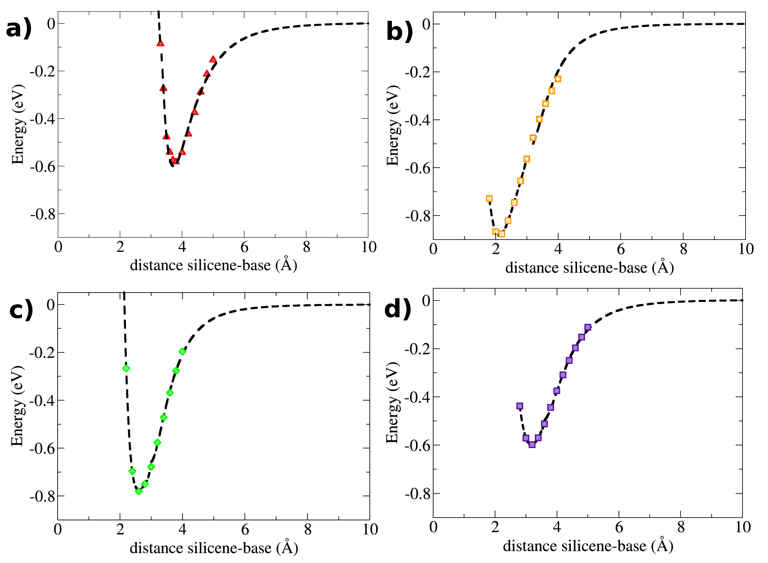
To explore the correlation between equilibrium height of the DNA nucleobases above the silicene substrate and the associated binding energy, we carried out a vertical height scan of the energy of the combined system (Figure 4). The binding energy was calculated from the difference in energy between the minimum of the fitted curve and the asymptotic limit for large distances. Cytosine is found to exhibit the strongest binding, followed closely by Guanine. Adenine and Thymine are both bound about equally strong with the lowest overall binding energies. The precise numerical values for the binding energies are provided in the last column of Table 2. Clearly, the lower binding energies are found for those two nucleobases (A and T) that are furthest away from silicene, as it could be expected.
5 Charge Density Redistribution
To better understand the processes occurring at the electronic structure level when a nucleobase interacts with silicene, we calculated how the charge density of the system changes when these two entities are brought together. Mathematically, the change in charge density is simply expressed as . In Figure 5 we plot the resulting isosurfaces of the calculated charge density difference in space for the four nucleobases physisorbed on silicene. Blue color indicates that possesses a negative value, meaning that electronic charge density has increased in this region under the physisorption/chemisorption processes, while red color means that is of positive value, indicating that the electronic charge density has been decreased in this region. It can be seen quite clearly from these plots that for adenine and thymine interacting with silicene (Figure 5a and d), charge redistribution is concentrated mainly to the nucleobase part and in a trivial manner: a shift distributed uniformly over the whole area of the nucleobase, which could be interpreted as an electrostatic repulsion (electronic charge density shifting away from the silicene sheet). The interaction of adenine and thymine with silicene could thus be characterized as weak and purely non-covalent. However, the situation is radically different for the cases of cytosine and guanine interacting with silicene. Here, we notice a complex redistribution of charge density both in the nucleobase part and in the silicene substrate (Figure 5b and c). The respective insets in panels b and c of the figure clearly show that the major charge density redistribution occurs along the connection between the single oxygen atom of these two nucleobases and a Si atom of silicene, suggesting the formation of a weak bond of partially covalent nature. In other words: cytosine and guanine appear to be at least weakly chemisorbed on silicene, while adenine and thymine are merely physisorbed (no sign of covalent interaction). It is interesting to note that S. Kilina et al.53 observed similar behavior for nucleobases adsorbed on a Cu(111) surface.
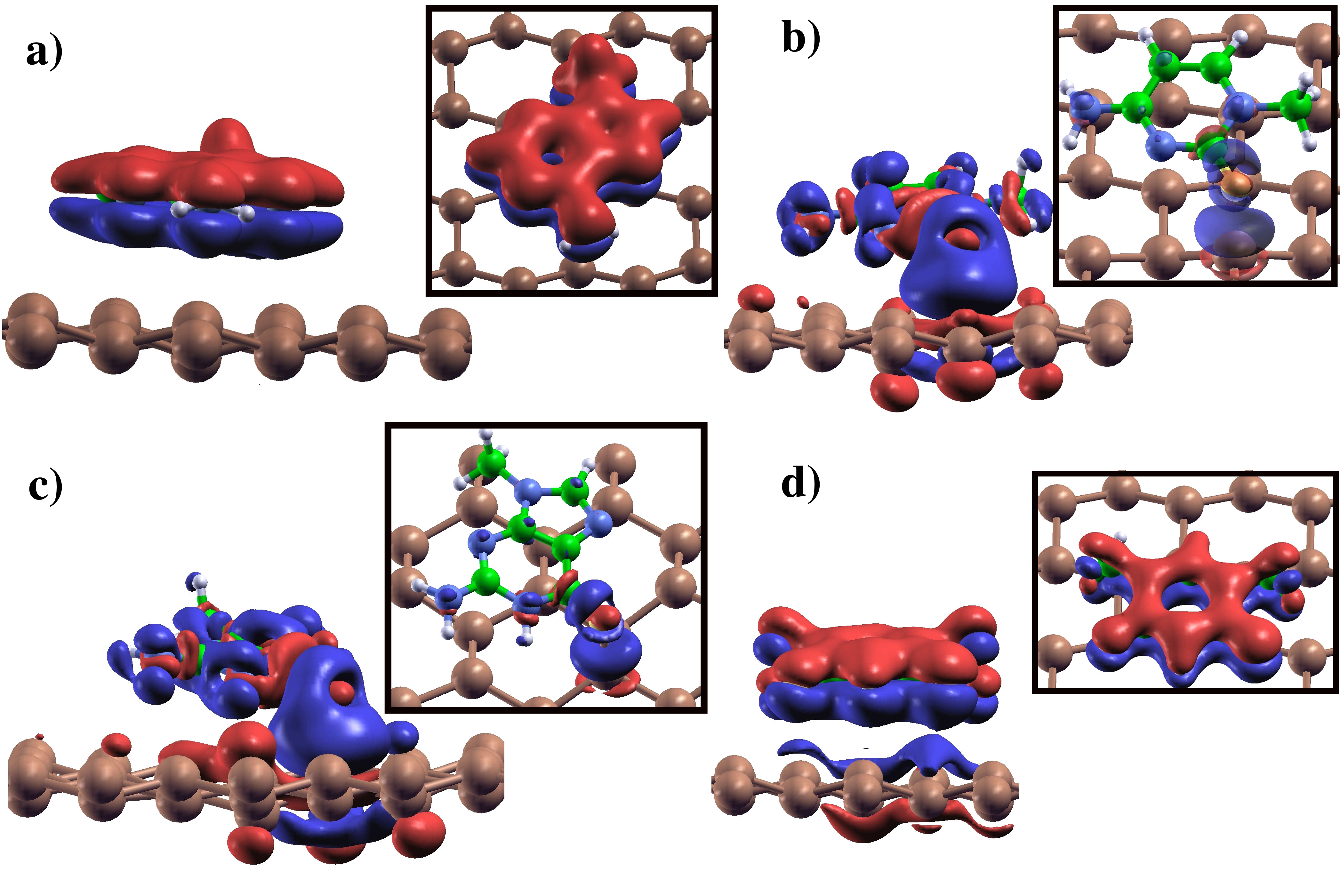
What is common for cytosine and guanine, the two bases that interact more strongly with silicene, is that they each possess one oxygen atom (Figure 3). It is via this oxygen atom that they form a quasi-covalent bond with a Si atom in silicene. The two nucleobases which are found by us not to interact strongly with silicene, adenine and thymine, possess either no oxygen atom (adenine) or two oxygen atoms (thymine). In the former case, it is trivially obvious that where there is no oxygen atom, no oxygen-mediated interaction between nucleobase and silicene can take place. And for thymine, forming two covalent bonds simultaneously with Si atoms through its two oxygen atoms is not possible for simple geometric reasons without enforcing any drastic distortions of the bond angles or bond lengths in thymine.
6 Effect on Electronic Transport
We finally come to the question whether silicene may possess any functionality for DNA sequencing. Stated in a more specific way, we are interested in how the electronic transport properties of silicene are affected when the four different nucleobases are physisorbed on its surface. We distinguish two possible transport directions, perpendicular to zigzag rows on the one hand, and perpendicular to armchair rows on the other hand (cf. Fig. 2c and 2d).
The energy-resolved transmittance indicates the probability of an electron to be transmitted from one electrode to the other via the scattering region in between. When analyzing in the following the changes in the zero-bias function upon adsorption of the nucleobases on silicene, it is important to remember the results of the equilibrium binding geometries presented above, which led us to identify two groups of nucleobases in terms of their silicene-nucleobase distance: group I (A and T) with a larger distance between silicene and nucleobase, and group II (C and G) with shorter distances and stronger coupling between the sole oxygen atom from the respective nucleobases and a protruding silicon atom in the buckled silicene sheet.

First, we discuss transport perpendicular to armchair rows (see Figure 6), concentrating on three energies: (i) eV, (ii) (which corresponds to the zero bias conductance of the system), and (iii) eV. For (i), we find decreases in the transmittance ranging from 5-15% for the nucleobases, allowing in principle to distinguish all the nucleobases from each other because the transmittance changes are quite characteristic. We note for (ii) that the transmittance is not changing for group I (A and T) compared with pristine silicene; however in group II (C and G) changes of 5% (7%) were seen in the transmittance. In the case for (iii) finally we again observe that it might be possible to distinguish C and G nucleobases, and in this case the decrease in transmission is even larger: about 15% (27%), respectively.

Next, we present the analogous analysis for transport perpendicular to zigzag rows (see Figure 7). Here, we are also concentrating on three energies: (i) eV and (ii) and (iii) are the same as in the previous case (i.e., and eV). In this case, there is a gap at the Fermi energy (see Figure 7). The interesting finding here is, for this setup we note that for (i) it is possible to distinguish the A and T nucleobases while for (iii) the other two nucleobases, C and G, show a decrease in the Transmission of 20-25%.
As expected, group II shows the larger change in transmittance due to the strong coupling with silicene, as seen in the charge density difference plots (cf. Figure 5). Group I exhibits a much smaller decrease in the transmittance due to weak interaction with silicene.

To clearly demonstrate that the diminution of the transmittance for C and G is due to the strong coupling between the oxygen atom from the nucleobase and silicene, we performed a transport calculation in a minimalistic model system consisting of an OH group bound with silicene (at the same distance as was found for the system silicene + nucleobase). The transmittance change for silicene when OH is bound to it is shown in Figure 8 (for comparison, the transmittance plots of C and G have also been reproduced here from Figure 6). We see that the addition of an OH group to silicene overall generates the same trend as that seen for C and G, thus confirming that the reduction in transmittance originates from the binding of oxygen to silicene.
7 Conclusions
In summary, we have presented here a comprehensive theoretical study about DNA nucleobases adsorbed on silicene and discussed a possible emerging application as a biosensor. Our computational results demonstrate that Adenine and Thymine are physisorbed on silicene, whereas Cytosine and Guanine are weakly chemisorbed through the formation of a Si–O bond. Simulated STM images can serve as a guide for experimentalists to recognize nucleobases on silicene. We also investigated the electronic transport using two setups, demonstrating that it is possible to distinguish the four nucleobases. For specific energies, the transmission of the nucleobases differs from that of pristine silicene in a characteristic manner. This result indicates that silicene may be a promising candidate for applications as a biosensor.
8 Methods
We combined ab initio density functional theory (DFT) 54, 55 as implemented in the SIESTA 56 code with the non-equilibrium Green’s function (NEGF) method from the TranSiesta code 57 to perform electronic transport calculations. To take into account weak dispersive interactions we employed a van der Waals correction 58, 59 to the Generalized Gradient Approximation (PBE-GGA) 60 for the exchange-correlation functional in DFT. A grid of -points were used for -space integration and the transport direction is aligned with the -axis. Furthermore, double- polarized basis sets (DZP) and norm-conserving pseudopotentials 61 were used. The conjugate gradient (CG) method was applied to obtain equilibrium structures with residual forces on atoms below eV/Å.
The principal idea of quantum transport calculations is to divide the system under investigation into three parts: two electrodes and a scattering region in between. Defining the boundary as a region where the charge density matches with the bulk electrodes and using localized basis sets, it is possible to write the non-equilibrium Green’s functions for the scattering region as:
| (1) |
where and are overlap matrix and Hamiltonian, respectively, for the scattering region and are self-energies that take into account the effect from the left (L) and right (R) electrode onto the central region. The self energies are given by , where are the surface Green’s functions for the semi-infinite leads and are the coupling matrix elements between the electrodes and the scatter region. The Hamiltonian can be calculated through a variety of approaches (e.g., using tight-binding methods), but really, is a functional of the electronic density, and for this reason, we used the Hamiltonian obtained from DFT calculations. The charge density is self-consistently calculated via Green’s functions until convergence is achieved at which point the transmission coefficient can be obtained:
| (2) |
where the coupling matrices are given by , with . Further details regarding the methods for calculating electronic transport properties can be found in the literature 57, 62.
Financial support from the Carl Tryggers Foundation and the Swedish Research Council (VR, Grant No. 621-2009-3628) is gratefully acknowledged. The Swedish National Infrastructure for Computing (SNIC) and the Uppsala Multidisciplinary Center for Advanced Computational Science (UPPMAX) provided computing time for this project.
Projected Densities of States for the combined system of DNA nucleobases adsorbed in silicene are presented in the supporting information.
![[Uncaptioned image]](/html/1404.2706/assets/TOC.jpg)
Structural view and simulated STM image for the nucleobase Adenine physisorbed on silicene. Electronic transport properties for all four DNA nucleobases on silicene are shown to the right.
References
- Takeda and Shiraishi 1994 Takeda, K.; Shiraishi, K. Theoretical possibility of stage corrugation in Si and Ge analogs of graphite. Physical Review B 1994, 50, 14916–14922
- Fagan et al. 2000 Fagan, S.; Baierle, R.; Mota, R.; da Silva, A.; Fazzio, a. Ab initio calculations for a hypothetical material: Silicon nanotubes. Physical Review B 2000, 61, 9994–9996
- Guzmán-Verri and Lew Yan Voon 2007 Guzmán-Verri, G.; Lew Yan Voon, L. Electronic structure of silicon-based nanostructures. Physical Review B 2007, 76, 075131
- Cahangirov et al. 2009 Cahangirov, S.; Topsakal, M.; Aktürk, E.; Şahin, H.; Ciraci, S. Two- and One-Dimensional Honeycomb Structures of Silicon and Germanium. Physical Review Letters 2009, 102, 236804
- Aufray et al. 2010 Aufray, B.; Kara, A.; Vizzini, S.; Oughaddou, H.; Leandri, C.; Ealet, B.; Le Lay, G. Graphene-like silicon nanoribbons on Ag(110): A possible formation of silicene. Applied Physics Letters 2010, 96, 183102
- Lalmi et al. 2010 Lalmi, B.; Oughaddou, H.; Enriquez, H.; Kara, A.; Vizzini, S.; Ealet, B.; Aufray, B. Epitaxial growth of a silicene sheet. Applied Physics Letters 2010, 97, 223109
- Lin et al. 2012 Lin, C.-L.; Arafune, R.; Kawahara, K.; Tsukahara, N.; Minamitani, E.; Kim, Y.; Takagi, N.; Kawai, M. Structure of Silicene Grown on Ag(111). Applied Physics Express 2012, 5, 045802
- Jamgotchian et al. 2012 Jamgotchian, H.; Colignon, Y.; Hamzaoui, N.; Ealet, B.; Hoarau, J. Y.; Aufray, B.; Bibérian, J. P. Growth of silicene layers on Ag(111): unexpected effect of the substrate temperature. Journal of physics. Condensed matter : an Institute of Physics journal 2012, 24, 172001
- Feng et al. 2012 Feng, B.; Ding, Z.; Meng, S.; Yao, Y.; He, X.; Cheng, P.; Chen, L.; Wu, K. Evidence of silicene in honeycomb structures of silicon on Ag(111). Nano letters 2012, 12, 3507–11
- Vogt et al. 2012 Vogt, P.; Padova, P. D.; Quaresima, C.; Avila, J.; Frantzeskakis, E. Silicene: Compelling Experimental Evidence for Graphenelike Two-Dimensional Silicon. Physical Review Letters 2012, 108, 155501
- Fleurence et al. 2012 Fleurence, A.; Friedlein, R.; Ozaki, T.; Kawai, H.; Wang, Y.; Yamada-Takamura, Y. Experimental Evidence for Epitaxial Silicene on Diboride Thin Films. Physical Review Letters 2012, 108, 245501
- Novoselov et al. 2004 Novoselov, K. S.; Geim, a. K.; Morozov, S. V.; Jiang, D.; Zhang, Y.; Dubonos, S. V.; Grigorieva, I. V.; Firsov, a. a. Electric field effect in atomically thin carbon films. Science (New York, N.Y.) 2004, 306, 666–9
- Branton et al. 2008 Branton, D.; Deamer, D. W.; Marziali, A.; Bayley, H.; Benner, S. a.; Butler, T.; Di Ventra, M.; Garaj, S.; Hibbs, A.; Huang, X. et al. The potential and challenges of nanopore sequencing. Nature biotechnology 2008, 26, 1146–53
- Fyta et al. 2011 Fyta, M.; Melchionna, S.; Succi, S. Translocation of biomolecules through solid-state nanopores: Theory meets experiments. Journal of Polymer Science Part B: Polymer Physics 2011, 49, 985–1011
- Venkatesan and Bashir 2011 Venkatesan, B. M.; Bashir, R. Nanopore sensors for nucleic acid analysis. Nature nanotechnology 2011, 6, 615–24
- Scheicher et al. 2012 Scheicher, R. H.; Grigoriev, A.; Ahuja, R. DNA sequencing with nanopores from an ab initio perspective. JOURNAL OF MATERIALS SCIENCE 2012, 47, 7439–7446
- Di Ventra 2013 Di Ventra, M. Fast DNA sequencing by electrical means inches closer. Nanotechnology 2013, 24, 342501
- Yang et al. 2013 Yang, Y.; Liu, R.; Xie, H.; Hui, Y.; Jiao, R.; Gong, Y.; Zhang, Y. Advances in Nanopore Sequencing Technology. JOURNAL OF NANOSCIENCE AND NANOTECHNOLOGY 2013, 13, 4521–4538
- Haque et al. 2013 Haque, F.; Li, J.; Wu, H.-C.; Liang, X.-J.; Guo, P. Solid-state and biological nanopore for real-time sensing of single chemical and sequencing of DNA. NANO TODAY 2013, 8, 56–74
- Postma 2010 Postma, H. W. C. Rapid sequencing of individual DNA molecules in graphene nanogaps. Nano letters 2010, 10, 420–5
- Merchant et al. 2010 Merchant, C. a.; Healy, K.; Wanunu, M.; Ray, V.; Peterman, N.; Bartel, J.; Fischbein, M. D.; Venta, K.; Luo, Z.; Johnson, a. T. C. et al. DNA translocation through graphene nanopores. Nano letters 2010, 10, 2915–21
- Schneider et al. 2010 Schneider, G. F.; Kowalczyk, S. W.; Calado, V. E.; Pandraud, G.; Zandbergen, H. W.; Vandersypen, L. M. K.; Dekker, C. DNA translocation through graphene nanopores. Nano letters 2010, 10, 3163–7
- Garaj et al. 2010 Garaj, S.; Hubbard, W.; Reina, a.; Kong, J.; Branton, D.; Golovchenko, J. a. Graphene as a subnanometre trans-electrode membrane. Nature 2010, 467, 190–3
- Nelson et al. 2010 Nelson, T.; Zhang, B.; Prezhdo, O. V. Detection of nucleic acids with graphene nanopores: ab initio characterization of a novel sequencing device. Nano letters 2010, 10, 3237–42
- Min et al. 2011 Min, S. K.; Kim, W. Y.; Cho, Y.; Kim, K. S. Fast DNA sequencing with a graphene-based nanochannel device. Nature nanotechnology 2011, 6, 162–5
- Cho et al. 2011 Cho, Y.; Min, S. K.; Kim, W. Y.; Kim, K. S. The origin of dips for the graphene-based DNA sequencing device. Physical chemistry chemical physics : PCCP 2011, 13, 14293–6
- Bergvall et al. 2011 Bergvall, A.; Berland, K.; Hyldgaard, P.; Kubatkin, S.; Lofwander, T. Graphene nanogap for gate-tunable quantum-coherent single-molecule electronics. PHYSICAL REVIEW B 2011, 84, 155451
- Sathe et al. 2011 Sathe, C.; Zou, X.; Leburton, J.-P.; Schulten, K. Computational Investigation of DNA Detection Using Graphene Nanopores. ACS NANO 2011, 5, 8842–8851
- He et al. 2011 He, Y.; Scheicher, R. H.; Grigoriev, A.; Ahuja, R.; Long, S.; Huo, Z.; Liu, M. Enhanced DNA Sequencing Performance Through Edge-Hydrogenation of Graphene Electrodes. Advanced Functional Materials 2011, 21, 2674–2679
- Prasongkit et al. 2011 Prasongkit, J.; Grigoriev, A.; Pathak, B.; Ahuja, R.; Scheicher, R. H. Transverse conductance of DNA nucleotides in a graphene nanogap from first principles. Nano Letters 2011, 11, 1941–5
- Liu et al. 2012 Liu, Y.; Dong, X.; Chen, P. Biological and chemical sensors based on graphene materials. Chemical Society reviews 2012, 41, 2283–307
- Saha et al. 2012 Saha, K. K.; Drndić, M.; Nikolić, B. K. DNA base-specific modulation of microampere transverse edge currents through a metallic graphene nanoribbon with a nanopore. Nano letters 2012, 12, 50–5
- Venkatesan et al. 2012 Venkatesan, B. M.; Estrada, D.; Banerjee, S.; Jin, X.; Dorgan, V. E.; Bae, M.-H.; Aluru, N. R.; Pop, E.; Bashir, R. Stacked Graphene-Al2O3 Nanopore Sensors for Sensitive Detection of DNA and DNA-Protein Complexes. ACS NANO 2012, 6, 441–450
- Cheng and Zhao 2012 Cheng, C.-L.; Zhao, G.-J. Steered molecular dynamics simulation study on dynamic self-assembly of single-stranded DNA with double-walled carbon nanotube and graphene. NANOSCALE 2012, 4, 2301–2305
- Qiu and Guo 2012 Qiu, H.; Guo, W. Detecting ssDNA at single-nucleotide resolution by sub-2-nanometer pore in monoatomic graphene: A molecular dynamics study. APPLIED PHYSICS LETTERS 2012, 100, 083106
- Wells et al. 2012 Wells, D. B.; Belkin, M.; Comer, J.; Aksimentiev, A. Assessing Graphene Nanopores for Sequencing DNA. NANO LETTERS 2012, 12, 4117–4123
- Liu et al. 2012 Liu, Y.; Dong, X.; Chen, P. Biological and chemical sensors based on graphene materials. CHEMICAL SOCIETY REVIEWS 2012, 41, 2283–2307
- Lv et al. 2013 Lv, W.; Chen, M.; Wu, R. The impact of the number of layers of a graphene nanopore on DNA translocation. SOFT MATTER 2013, 9, 960–966
- Garaj et al. 2013 Garaj, S.; Liu, S.; Golovchenko, J. A.; Branton, D. Molecule-hugging graphene nanopores. Proceedings of the National Academy of Sciences of tThe United States of America 2013, 110, 12192–12196
- Li et al. 2013 Li, J.; Zhang, Y.; Yang, J.; Bi, K.; Ni, Z.; Li, D.; Chen, Y. Molecular dynamics study of DNA translocation through graphene nanopores. PHYSICAL REVIEW E 2013, 87, 062707
- Hui et al. 2013 Hui, Z.; Xiang, N.; Sheng-Lin, P.; Jun, O.; Yu, C.; Fang-Ping, O. First-Principles Study of Graphene-Based Biomolecular Sensor. ACTA PHYSICO-CHIMICA SINICA 2013, 29, 250–254
- Avdoshenko et al. 2013 Avdoshenko, S. M.; Nozaki, D.; da Rocha, C. G.; Gonzalez, J. W.; Lee, M. H.; Gutierrez, R.; Cuniberti, G. Dynamic and Electronic Transport Properties of DNA Translocation through Graphene Nanopores. NANO LETTERS 2013, 13, 1969–1976
- Prasongkit et al. 2013 Prasongkit, J.; Grigoriev, A.; Pathak, B.; Ahuja, R.; Scheicher, R. H. Theoretical Study of Electronic Transport through DNA Nucleotides in a Double-Functionalized Graphene Nanogap. JOURNAL OF PHYSICAL CHEMISTRY C 2013, 117, 15421–15428
- Jeong et al. 2013 Jeong, H.; Kim, H. S.; Lee, S.-H.; Lee, D.; Kim, Y. H.; Huh, N. Quantum interference in DNA bases probed by graphene nanoribbons. APPLIED PHYSICS LETTERS 2013, 103, 023701
- Freedman et al. 2013 Freedman, K. J.; Ahn, C. W.; Kim, M. J. Detection of Long and Short DNA Using Nanopores with Graphitic Polyhedral Edges. ACS NANO 2013, 7, 5008–5016
- Schneider et al. 2013 Schneider, G. F.; Xu, Q.; Hage, S.; Luik, S.; Spoor, J. N. H.; Malladi, S.; Zandbergen, H.; Dekker, C. Tailoring the hydrophobicity of graphene for its use as nanopores for DNA translocation. NATURE COMMUNICATIONS 2013, 4, 2619
- Traversi et al. 2013 Traversi, F.; Raillon, C.; Benameur, S. M.; Liu, K.; Khlybov, S.; Tosun, M.; Krasnozhon, D.; Kis, A.; Radenovic, A. Detecting the translocation of DNA through a nanopore using graphene nanoribbons. Nature Nanotechnology 2013, 8, 939–945
- Mukhopadhyay et al. 2010 Mukhopadhyay, S.; Gowtham, S.; Scheicher, R. H.; Pandey, R.; Karna, S. P. Theoretical study of physisorption of nucleobases on boron nitride nanotubes: a new class of hybrid nano-biomaterials. Nanotechnology 2010, 21, 165703
- Lee et al. 2013 Lee, J.-H.; Choi, Y.-K.; Kim, H.-J.; Scheicher, R. H.; Cho, J.-H. Physisorption of DNA Nucleobases on h -BN and Graphene: vdW-Corrected DFT Calculations. The Journal of Physical Chemistry C 2013, 117, 13435–13441
- Gowtham et al. 2007 Gowtham, S.; Scheicher, R.; Ahuja, R.; Pandey, R.; Karna, S. Physisorption of nucleobases on graphene: Density-functional calculations. Physical Review B 2007, 76, 033401
- Horcas et al. 2007 Horcas, I.; Fernández, R.; Gómez-Rodríguez, J. M.; Colchero, J.; Gómez-Herrero, J.; Baro, a. M. WSXM: a software for scanning probe microscopy and a tool for nanotechnology. The Review of scientific instruments 2007, 78, 013705
- Tersoff, J and Hamann 1985 Tersoff, J and Hamann, D. R. Theory of the scanning tunneling microscope. Phys. Rev. B 1985, 31, 805
- Kilina et al. 2007 Kilina, S.; Tretiak, S.; Yarotski, D.; Zhu, J.-X.; Modine, N.; Taylor, a.; a.V. Balatsky, Electronic Properties of DNA Base Molecules Adsorbed on a Metallic Surface. Journal of Physical Chemistry C 2007, 111, 14541–14551
- Hohenberg and Kohn 1964 Hohenberg, P.; Kohn, W. Inhomogeneous electron gas. Physical Review 1964, 155
- Kohn and Sham 1965 Kohn, W.; Sham, L. Self-consistent equations including exchange and correlation effects. PHYSICAL REVIEW 1965, 385
- Soler et al. 2002 Soler, M.; Artacho, E.; Gale, J. D.; Garc, A.; Junquera, J.; Ordej, P.; Daniel, S. The SIESTA method for ab initio order- N materials. J. Phys.: Condens. Matter 2002, 2745, 2745–2779
- Brandbyge et al. 2002 Brandbyge, M.; Mozos, J.-L.; Ordejón, P.; Taylor, J.; Stokbro, K. Density-functional method for nonequilibrium electron transport. Physical Review B 2002, 65, 165401
- Dion et al. 2004 Dion, M.; Rydberg, H.; Schröder, E.; Langreth, D. C.; Lundqvist, B. I. Van der Waals Density Functional for General Geometries. Physical Review Letters 2004, 92, 246401
- Román-Pérez and Soler 2009 Román-Pérez, G.; Soler, J. Efficient Implementation of a van der Waals Density Functional: Application to Double-Wall Carbon Nanotubes. Physical Review Letters 2009, 103, 096102
- Perdew et al. 1996 Perdew, J. P.; Burke, K.; Ernzerhof, M. Generalized Gradient Approximation Made Simple. PHYSICAL REVIEW LETTERS 1996, 77, 3865–3868
- Troullier 1991 Troullier, N. Efficient pseudopotentials for plane-wave calculations. Phys. Rev. B 1991, 43, 1993–2006
- Rocha et al. 2006 Rocha, a.; García-Suárez, V.; Bailey, S.; Lambert, C.; Ferrer, J.; Sanvito, S. Spin and molecular electronics in atomically generated orbital landscapes. Physical Review B 2006, 73, 085414