Fingerprints of Inelastic Transport at the Surface of Topological Insulator Bi2Se3: Role of Electron-Phonon Coupling
Abstract
We report on electric-field and temperature dependent transport measurements in exfoliated thin crystals of Bi2Se3 topological insulator. At low temperatures ( K) and when the chemical potential lies inside the bulk gap, the crystal resistivity is strongly temperature dependent, reflecting inelastic scattering due to the thermal activation of optical phonons. A linear increase of the current with voltage is obtained up to a threshold value at which current saturation takes place. We show that the activated behavior, the voltage threshold and the saturation current can all be quantitatively explained by considering a single optical phonon mode with energy meV. This phonon mode strongly interacts with the surface states of the material and represents the dominant source of scattering at the surface at high electric fields.
The observation of surface states protected by time inversion invariance in the Bi2Se3 family of materials hasan10 ; moore10 ; zhang11 ; brune11 ; xia09 ; zhang09 , have triggered intense research because of the possibility of developing topological insulator (TI) devices at room temperature. However, the properties limiting charge transport, which is key for electronic applications, are still not known in detail. Elastic scattering by disorder imposes a limit to the conductivity of the surface states at low temperatures, nevertheless, as disorder is reduced, the limit at finite temperatures will be ultimately set by the intrinsic electron-phonon (e-ph) coupling. In recent theoretical work a strong e-ph coupling in Bi2Te3 was obtained egger11 ; giraud12 . The results are in agreement with temperature-dependent angle-resolved photoemission spectroscopy (ARPES) measurements in Bi2Se3 hofmann11 ; zhou13 . ARPES studies target the electronic structure and integrate the e-ph interaction over all phonon modes. The main dispersive surface optical-phonon branch with an energy of about 6 to 8 meV at the point was identified using helium-beam surface scattering, which also showed the absence of Rayleigh phonons batanouny11 . The e-ph coupling constant for this branch was found to be larger than any of the integrated values that are reported with ARPES batanouny12 . Such results are further supported by magneto-optical basov10 and Fourier-transform interferometry dipietro13 which found an optical phonon mode at meV.
Experimental investigations therefore suggest an anomalously large e-ph coupling for a specific surface-phonon branch, which could be readily observable in electrical transport measurements, wu13 in particular because surface states in Bi2Se3 carry a large fraction of the current flowing in thin crystals peng09 ; steinberg10 ; ong11 ; sacepe11 ; xiu11 and films steinberg11 ; kandala13 . Additionally, the calculated bulk phonon dispersion curves projected into the surface Brillouin zone also show an optical phonon in the same energy range batanouny11 . However, no fingerprint of an optical phonon mode on inelastic transport has been reported to date.
In this Letter, by performing temperature and voltage dependent transport measurements in Bi2Se3 thin crystals, a strong electron-phonon mediated inelastic backscattering phenomenon is unveiled. For temperatures K ( is the Boltzmann constant), the resistance is highly nonlinear and is consistent with a thermally-activated behavior dictated by an optical phonon with meV, as identified in spectroscopic experiments batanouny11 ; batanouny12 ; basov10 ; dipietro13 . Moreover, the onset of suppression of the conductance for meV, in conjunction with current saturation as reported in graphene meric08 ; barreiro09 ; Foa2006 , further confirm the influence of a meV mode.
The devices were fabricated with single crystals mechanically exfoliated onto a highly-doped Si substrate with 280 nm or 440 nm of thermally grown SiO2, followed by e-beam lithography, metal deposition, and lift-off. The inset of Fig. 1(c) shows an optical microscope image of a typical device used in the present study. The chosen crystals have elongated shape to obtain a homogeneous current flow. The distances between the inner and outer electrodes are about 0.3 - 1 m and 2 - 3 m, respectively. Four-probe transport measurements down to 4.2 K were performed on six different devices in vacuum, yielding similar results (Table SI SI ). Here we present representative data for two of them with nm (device D1) and nm (device D2).
Figures 1(a) and (b) show the square resistance as a function of gate voltage for devices D1 and D2, respectively. When sweeping from positive to negative values, an increase in is observed, which is due to the -type doping commonly observed in Bi2Se3 crystals. Figure 1(c) shows versus temperature for device D1 at three gate voltages (+30, -60, and -100 V) and nA. For = 30 V, is weakly temperature dependent, presumably because the chemical potential lies inside the conduction band and disorder scattering is dominant ong11 . In contrast, the temperature dependence of becomes highly nonlinear when is shifted towards the material bulk gap, where the surface transport is expected to dominate steinberg10 ; ong11 . This is evident for = -60 and -100 V and from weak localization measurements ong11 ; steinberg11 .
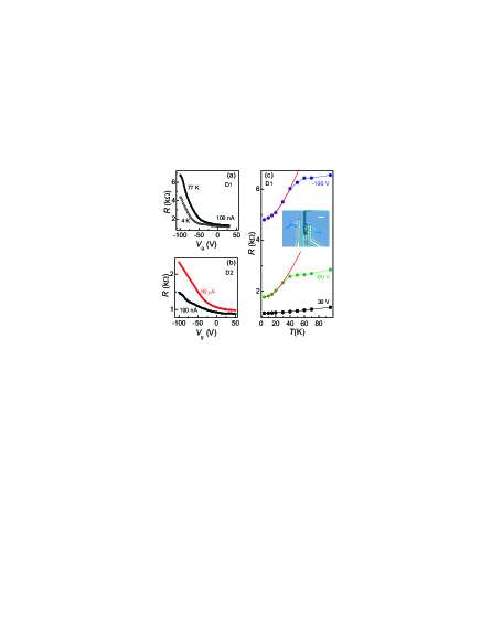
When lies inside the gap, the conductance splits in surface and bulk contributions, , where results from carriers excitation to the conduction or valence bands, which is more significant for K ong11 ; fuhrer12 . Hence, the strong temperature dependence for negative at K suggests an activated process at the surface mediated by inelastic scattering involving a single or multiple phonon modes. Our data can be indeed fitted (red lines on Fig. 1c) with an equation that only includes a single Bose-Einstein term, thus a single phonon mode, as follows:
| (1) |
where the first term accounts for low temperature (residual) resistance due to scattering on static impurities or defects, while the second term is associated to acoustic phonons, for which a linear resistance with temperature has been predicted egger11 and recently observed fuhrer12 .
In Eq. (1), and are fitting parameters, where is independent on for carriers with a linear dispersion relation, that is, for Dirac fermions at the surface fuhrer08 . The best fit gives meV which corresponds to the energy of the dominant surface phonon branch observed by helium-beam surface scattering batanouny12 and optical methods basov10 ; dipietro13 . It could also be due to scattering off bulk optical phonons projected into the surface batanouny11 . The fit however is not enough proof to demonstrate that the main scattering mechanism originates from an optical phonon branch. A power-law dependence expected in some cases for acoustic phonons scattering can also fit the results, and therefore further experiments are necessary SI .
An activated response similar to that in Fig. 1c was found in graphene on a SiO2 substrate fuhrer08 . It was argued to originate from remote interfacial phonon scattering by surface optical phonon modes in SiO2. Because the lowest energy of the relevant modes exceeds 50 meV, much larger than that in Bi2Se3, the activated behavior was only observed at K. Additionally, the same nonlinear -dependence of was noted in Ca-doped Bi2Se3 crystals and its onset with was interpreted as reaching the lower edge of the conduction band ong11 , however the activated nature of the effect was not discussed SI .
Electrical transport experiments in graphene have shown that the current tends to saturate as the bias voltage is increased above meV meric08 ; barreiro09 ; Foa2006 . The saturation has been attributed to scattering of electrons by optical phonons, either activated at the SiO2 surface meric08 ; scharf13 or intrinsic to graphene barreiro09 . If the activation energy observed in Fig. 1c was due to an optical phonon mode, the current in Bi2Se3 should also tend to saturate with . Such saturation behavior is expected for scattering of electrons by optical phonons but not for acoustic phonons. Additionally, the saturation current should be weakly temperature dependent.
A first indication of sublinear - response is observed in Fig. 1b, where an increase in is evident when a large current A is applied. The fact that the relative change of is much larger when is shifted towards the bulk gap ong11 supports that the main phenomenon is surface related.
Figures 2 and 3 show our main results. Figure 2 displays the - characteristics for different gate voltages at 4.2 K. The current at large negative presents a clear tendency for saturation at mV, with a smaller saturation current for larger absolute values of . This behavior is consistent with optical-phonon scattering and resembles the behavior observed in graphene, where the current saturation becomes gate dependent and decreases when approaching the Dirac point meric08 ; barreiro09 . However, also shows a kink at mV. As discussed below, this feature is likely to be associated to carrier excitations into the conduction and/or valence bands.
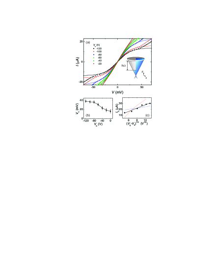
Because the saturation is not complete, we approximate by a saturation model for further analysis. Having compared the fit of our data with different analytical expressions meric08 ; canali75 ; sze85 ; Pop10 , we found that, as in graphene Pop10 , the best results are obtained using , where is the gate-dependent conductance at low , and and the saturation current are fitting parameters. We fitted the data up to the position of the kink , which is determined by the minimum in SI . The gate-dependence of is shown in Fig. 2b. The above equation with gives the best fit, regardless of the value of (lines in Fig. 2a); the extracted values of are shown in Fig. 2c.
In order to model , we note that, for instantaneous phonon emission, a steady-state population is established in which right moving electrons are populated to a higher energy than left moving ones yao00 ; barreiro09 (see inset of Fig. 2a). can then be estimated by integrating the electrons velocity over the steady state population, which for Dirac fermions and two coupled surfaces results in barreiro09 ; Eq1 :
| (2) |
where is the width of the sample and , the backgate capacitance. is the gate voltage at which is tuned at the Dirac point.
Even though we cannot access , because the threshold for breakdown of the SiO2 dielectric is reached first, direct comparison with results in Ca-doped Bi2Se3 crystals ong11 together with the incipient rounding of the response (Figs. 1b and 1c) suggest that is within a few tens of volts beyond the breakdown. Indeed, Eq. (2) gives a good fit to vs with V (Fig. 2c). From the fit, we obtain meV, which is in remarkable agreement with the activation energy estimated from the data in Fig. 1. Additionally, Fig. 2c shows the large discrepancy between the experimental data and the theoretical using Eq. (2) for equal to 5 meV and 12 meV, which further yield unrealistic values of (-245 V and -120 V, respectively). This demonstrates that must be in a very restricted range of energies.
Figure 3 shows the conductance at specific gate voltages. At high positive , presents a smooth decrease with , which is typical of a bulk metal in which the dominant scattering mechanism is disorder. At large negative , when activation effects in Fig. 1 become evident, develops a plateau-like feature under the action of a weak electric field. There, the only contribution to the resistance comes from elastic scattering induced by static disorder. The increase of the bias voltage leads to an energy gain by the propagating electrons, which eventually reaches the energy threshold that allows for an electron-phonon scattering event (such as phonon emission). A new inelastic transport length scale then enters into play and brings about an additional contribution to the resistance, which adds up to the elastic one, in virtue of the Matthiessen rule. At fixed gate voltage (or Fermi level position), the elastic part is given by the measured resistance at low-temperature and zero-bias, whereas the inelastic contribution is bias-dependent. The onset for phonon scattering occurs at about 10 mV (pinpointed by vertical lines in Figs. 3 and 4), while in this crystal the suppression of the conductance becomes significant only beyond 20-30 mV.
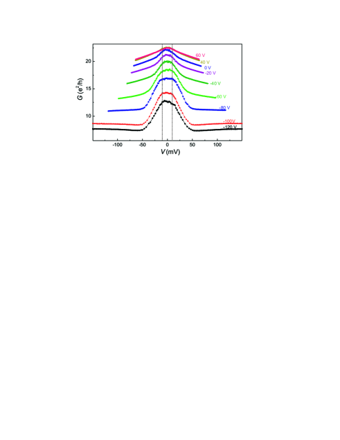
We now focus on the origin of the kink in the - characteristics (Fig. 2a). The position of the kink , which is given in Fig. 2b, is weakly dependent on for V, but drops quickly as approaches zero, becoming undetectable for positive , which coincides with .
The kink can be due to excitations of carriers into the conduction and/or valence bands ong11 ; fuhrer12 ; wu13 . A similar gate-driven transformation to a conductor with strong temperature dependence (Fig. 1c) was reported in Ref. ong11, and associated to the opening of an effective bulk gap meV that results from gap narrowing due to band bending (the intrinsic bulk gap in Bi2Se3 is about 300 meV). At low temperatures, the presence of such gap is essential for observing signatures of surface states. However, at high enough temperatures, thermal excitation of carriers from remnant electron pockets to the conduction band can enhance the bulk transport contribution ong11 ; SI . The transfer of electrons from the electron pockets to the conduction band can also be driven by high electric fields, which for meV exceed 1 kV/cm. Such transitions are known to occur in GaAs between conduction valleys sze85 . This explanation is further supported by the increase of as the chemical potential is moved deeper into the gap; however the weak dependence for V remains unexplained. Thermal activation of a bulk channel was also observed in Ref. fuhrer12, , but ascribed to the activation of electrons from the bulk valence band to the surface band. It is plausible that the overall response of results from the combination of these two phenomena, and thus V may signal the onset of electron transfer from the valence band that prevents from further increasing.
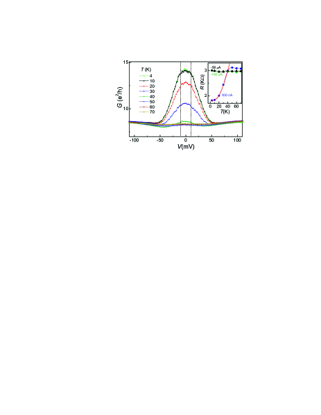
Figure 4 displays at V for between 4.2 K and 70 K. is strongly temperature dependent for mV. Over this range and for K, presents the same activated behavior that is observed at low , with a characteristic energy of about 8 meV (inset). In contrast, is largely temperature independent for mV. This is typical of a disordered metal, a behavior that was found when lies in the bulk conduction band (Fig. 1c), which is in agreement with the hypothesis of electron transfer into bulk channels. Finally, the observation of being nearly independent of despite significant change in , further supports the origin of the saturation as being related to a single optical phonon branch SI .
In conclusion, our results show compelling evidence of a strong e-ph coupling involving an optical phonon mode with meV that mediates inelastic scattering. The thermally activated behavior of the Bi2Se3 resistance at low temperatures, the voltage at which inelastic scattering emerges, and the magnitude of the saturation current at high voltage and its independence of temperature are all consistent with this interpretation. This is reinforced by helium scattering experiments, which identified a main phonon mode at 6-8 meV and the absence of acoustic Rayleigh phonons batanouny11 ; batanouny12 , and theoretical calculations that show a bulk optical phonon that projects into the surface Brillouin zone in the same energy range batanouny11 . The transport experiments carried out here are in a less controlled environment than those in Refs. batanouny11 ; batanouny12 . However, the surface states in Bi2Se3 have proven to be robust to processing and, in particular, the relevant surface phonon mode was observed even after exposure to air basov10 .
We acknowledge the support from the European Research Council (ERC Grant agreement 308023 SPINBOUND) MINECO (MAT2010-18065 and MAT2012-33911, RYC-2011-08319) and AGAUR (Beatriu de Pinós program).
References
- (1) M. Z. Hasan and C. L. Kane, Rev. Mod. Phys. 82, 3045 (2010).
- (2) X.-L. Qi and S.-C. Zhang, Rev. Mod. Phys. 83, 1057 (2011).
- (3) J. E. Moore, Nature (London) 464, 194 (2010).
- (4) C. Brüne, C. X. Liu, E. G. Novik, E. M. Hankiewicz, H. Buhmann, Y. L. Chen, X. L. Qi, Z. X. Shen, S. C. Zhang, and L. W. Molenkamp Phys. Rev. Lett. 106, 126803 (2011).
- (5) Y. Xia, D. Qian, D. Hsieh, L. Wray, A. Pal, H. Lin, A. Bansil, D. Grauer, Y. S. Hor, R. J. Cava, and M. Z. Hasan, Nat. Phys. 5, 398 (2009).
- (6) H. J. Zhang, C. X. Liu, X. L. Qi, X. Dai, Z. Fang, and S. C. Zhang, Nat. Phys. 5, 438 (2009).
- (7) S. Giraud, and R. Egger, Phys. Rev. B 83, 245322 (2011).
- (8) S. Giraud, A. Kundu, and R. Egger, Phys. Rev. B 85, 035441 (2012)¨.
- (9) R. C. Hatch, M. Bianchi, D. Guan, S. Bao, J. Mi, B. B. Iversen, L. Nilsson, L. Hornekaer, and P. Hofmann, Phys. Rev. B 83, 241303 (2011).
- (10) C. Chen et al., arXiv:1302.0123 [cond-mat.str-el] (2013).
- (11) X. Zhu, L. Santos, R. Sankar, S. Chikara, C. . Howard, F. C. Chou, C. Chamon, and M. El-Batanouny, Phys. Rev. Lett. 107, 186102 (2011).
- (12) X. Zhu, L. Santos, C. Howard, R. Sankar, F. C. Chou, C. Chamon, and M. El-Batanouny, Phys. Rev. Lett. 108, 185501 (2012).
- (13) A. D. LaForge, A. Frenzel, B. C. Pursley, T. Lin, X. Liu, J. Shi, and D. N. Basov, Phys. Rev. B 81, 125120 (2010).
- (14) P. Di Pietro et al., Nat. Nano. (2013).
- (15) P. Zhang and M. W. Wu,Phys. Rev. B 87, 085319 (2013).
- (16) H. Peng et al. Nat. Mat. 9, 225, (2009).
- (17) H. Steinberg, D. R. Gardner, Y. S. Lee, and P. Jarillo-Herrero, Nano Lett. 10, 5032 (2010)
- (18) J.G. Checkelsky, Y.S. Hor, R.J. Cava, and N.P. Ong, Phys. Rev. Lett. 106, 196801 (2011).
- (19) B. Sacepe, J.B. Oostinga, J. Li, A. Ubaldini, N.J.G. Couto, E. Giannini, and A.F. Morpurgo, Nat. Commun. 2, 575, (2011).
- (20) F. Xiu et al. Nat. Nano. 6, 216, (2011).
- (21) H. Steinberg, J. -B. Laloe, V. Fatemi, J. S. Moodera, and P. Jarillo-Herrero, Phys. Rev. B 84, 233101 (2011).
- (22) A. Kandala , A. Richardella , D. Zhang , T. C. Flanagan, and N. Samarth, Nano Lett. 13, 2471 (2013).
- (23) I. Meric, M. Y. Han, A. F. Young, B. Özyilmaz, P. Kim and K. L. Shepard, Nat. Nano. 3, 654 (2008).
- (24) B. Scharf, V. Perebeinos, J. Fabian, and I. Z̆utić, arXiv:1307.4008 [cond-mat.mes-hall] (2013), Phys. Rev. B 88, 125429 (2013).
- (25) A. Barreiro, M. Lazzeri, J. Moser, F. Mauri, and A. Bachtold Phys. Rev. Lett. 103, 076601 (2009).
- (26) In deriving the Eq. (2), we considered the second expression of Eq. (1) from Ref. barreiro09 ; due to the low energy of the relevant phonon modes we assumed , a condition that is later verified by the fitting results.
- (27) L.E.F. Foa Torres, S Roche, Phys. Rev. Lett. 97, 076804 (2006).
- (28) See Suplimentary Material at … for more experimental data and discussion.
- (29) D. Kim, Q. Li, P. Syers, N. P. Butch, J. Paglione, S. Das Sarma, and M. S. Fuhrer, Phys. Rev. Lett. 109, 166801 (2012).
- (30) J. H. Chen, C. Jang, S. Xiao, M. Ishigami, and M. S. Fuhrer, Nat. Nano. 3, 206 (2008).
- (31) C. Canali, G. Majni, R. Minder, and G. Ottavianni, IEEE Trans. Electron. Dev. 22, 1045 (1975).
- (32) S. M. Sze, Semiconductor Devices (John Wiley and Sons, New York, 1985).
- (33) V. E. Dorgan, M.-H. Bae, and E. Pop, Appl. Phys. Lett. 97, 082112 (2010).
- (34) Z. Yao, C. L. Kane, and C. Dekker, Phys. Rev. Lett. 84, 2941 (2000).