University of New South Wales]School of Physics, University of New South Wales, Sydney NSW 2052, Australia Australian National University] Department of Electronic Materials Engineering, Research School of Physics and Engineering, The Australian National University, Canberra ACT 0200, Australia Lund University]Solid State Physics/Nanometer Structure Consortium (nmC@LU), Lund University S-221 00 Lund, Sweden University of New South Wales]School of Physics, University of New South Wales, Sydney NSW 2052, Australia
Electron-beam patterning of polymer electrolyte films to make multiple nanoscale gates for nanowire transistors
Abstract
We report an electron-beam based method for the nanoscale patterning of the poly(ethylene oxide)/\ceLiClO4 polymer electrolyte. We use the patterned polymer electrolyte as a high capacitance gate dielectric in single nanowire transistors and obtain subthreshold swings comparable to conventional metal/oxide wrap-gated nanowire transistors. Patterning eliminates gate/contact overlap which reduces parasitic effects and enables multiple, independently controllable gates. The method’s simplicity broadens the scope for using polymer electrolyte gating in studies of nanowires and other nanoscale devices.
Keywords: III-V nanowires, polymer electrolytes, electron beam lithography, nanoelectronics.
Polymer electrolytes 1 and III-V nanowire transistors 2, 3 are two exciting outcomes of recent research on nanoscale devices and novel electronic materials. A polymer electrolyte typically consists of a salt dissolved in a solid polymeric matrix, e.g., \ceLiClO4 in poly(ethylene oxide) (PEO) 4; they are commonly used as a gate dielectric in organic field-effect transistors. The electric field resulting from a voltage applied to the gate drives motion of \ceLi+ and \ceClO4- ions through the polymer matrix to form an electric double layer (EDL) at the gate/insulator and insulator/channel interfaces. EDL formation effectively transfers the gate charge to nm away from the channel, 5 producing the high dielectric constants and specific capacitances for which polymer electrolyte gate dielectrics are known. 1 The benefits of reduced operating voltages 6 and enhanced carrier density 7 that polymer electrolytes bring to organic transistors have seen them applied to one-dimensional nanomaterials also; first with carbon nanotubes, 8, 9, 10 and more recently, with self-assembled InAs nanowires. 11 The latter is part of a broader quest to improve electrostatic gate control in nanowire-based devices, both for fundamental transport studies and potential nanowire device applications.
The first nanowire transistors were gated using a \ceSiO2-coated, degenerately-doped Si substrate; though effective, this approach provides no local control over carrier density. 12 Subsequent work led to patterned local gating of laterally-oriented nanowires via electrodes both under 13 and over 14 the nanowire, and more recently, with a concentric ‘wrap-gate’ 15, 16. Wrap-gates provide more homogeneous carrier depletion and better gate/channel coupling 17, give improved subthreshold characteristics and reduced operating voltage, 18, 15, 16 and enable more controllable devices for fundamental studies of 1D transport. 19, 20, 21
Liang and Gao’s use of a PEO/\ceLiClO4 polymer electrolyte gate spin-coated over an InAs nanowire provides a simpler route to lateral wrap-gated nanowire transistors; 11 however, a key limitation resides in a lack of methods for nanoscale patterning of polymer electrolytes. Patterning the polymer electrolyte is desirable to avoid it overlapping the source/drain contacts, which can lead to parasitic capacitance, leakage currents and contact corrosion 1. It also enables independent contacting of multiple devices on the same chip. The micron-scale resolution of established polymer electrolyte deposition methods, e.g., ink-jet printing, 22, 23 injection into microfluidic channels 10 and photolithography, 24 presently limits the use of polymer electrolytes in nanowire transistors, where nm - m channel lengths are typical. Here we report the development of a process for electron-beam patterning of the PEO/\ceLiClO4 polymer electrolyte, and demonstrate the versatility it provides by making nanoscale-patterned single and double electrolyte-gated nanowire transistors. This nanoscale patterning capability enables us to produce multiple independent devices, each with multiple independently controllable electrolyte gates, on a single chip.
Electron Beam Lithography (EBL) is a widely used tool for nanoscale patterning; it relies on using electron-induced chain scission/crosslinking to locally alter the solubility of a polymeric ‘resist’ layer in a ‘developer’ solution. PEO can be crosslinked by exposure to energetic electrons, which makes these regions comparatively insoluble in developers such as tetrahydrofuran, methanol and \ceH2O; as such PEO is a negative-tone EBL resist, though not widely used practically. Krsko et al. first demonstrated EBL of PEO, 25 with feature sizes down to nm achieved soon thereafter 26. These works used PEO with molecular weights (MW) of and k without any added salts, and keV electrons at doses C/m2. In implementing EBL-patterning of a polymer electrolyte there are some new concerns that arise, e.g., whether the added salt either captures incident electrons or adversely affects electron-induced crosslinking, and whether the cross-linked PEO remaining after development has sufficient ionic mobility to produce a functional device. While EBL patterning of salt-doped PEO for nanoscale functional polymer electrolyte gates has not been previously demonstrated, prior research suggests its viability, e.g., electron-beam crosslinking has been used to enhance ionic conductivity in solid polymer electrolytes for battery applications. 27, 28
Polymer electrolytes were formed by mixing PEO (Aldrich, MW k) and \ceLiClO4.3H2O (Aldrich) in polymer:salt ratios of , and by sonication in mL of methanol. The resulting mixture was left standing at room temperature overnight to precipitate out large particulates, with the supernatant used for deposition. The solution was spun onto the sample at rpm for s and the sample was then baked on a hot-plate at C for mins. The resulting film was EBL patterned using either an FEI Sirion for preliminary experiments (Fig. 1), or a Raith -Two for nanowire device fabrication (Figs 2-4). Patterning was performed using a kV accelerating voltage and beam currents of pA under high vacuum. The patterned films were developed in deionized water at room temperature for s and dried with \ceN2 gas.
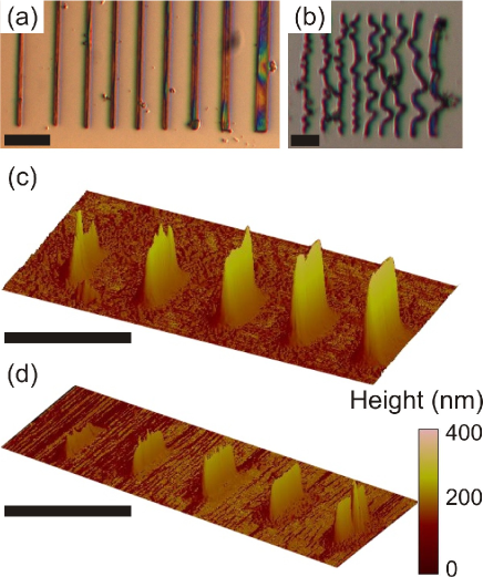
The optical micrograph in Fig. 1(a) shows PEO/\ceLiClO4 patterned at an electron dose C/m2 into lines with different defined line widths, aimed at establishing the patternability of PEO/\ceLiClO4 films using EBL, and an initial assessment of resolution limit. Pattern broadening is common for negative tone EBL resists and is caused by the proximity effect – the same physics produces the undercut profile for positive tone EBL resists such as polymethylmethacrylate (PMMA). 29, 30 This means that the final pattern dimensions can be significantly greater than the region scanned by the electron beam. Thus, two line widths are important: the ‘defined’ line width, , as written by the electron beam, and the measured line width after development, , which we take as the full width at half maximum determined by atomic force microscopy. The proximity effect can also result in depending strongly on dose: This is suggested in Fig. 1(a), where there is a clear difference in measured line width for wider lines ( nm) but saturates for nm with C/m2. We used atomic force microscopy to study the effects that electron dose, polymer:salt ratio and substrate material have on the shape and dimensions of structures remaining after development.
Figures 1(c/d) show nm lines exposed at C/m2 for two polymer:salt ratios (Fig. 1(c)) and (Fig. 1(d)). Focussing first on dose, in Fig. 1(c) decreases continuously from m to nm as is reduced from C/m2 to C/m2. This is expected for proximity effect controlled line-width. Looking more closely at the base-broadening, the width at the substrate can be up to , but the profiles in Fig. 1(c) show that most of the broadening occurs for heights nm above the substrate surface. This suggests the broadening arises due to surface effects, and as such, the base width may be controllable with surface treatments; we will address this in future work. The reduction of with lower would imply that minimizing is most optimum but there are two additional factors that weigh against this: line height and surface adhesion. First and foremost, the line height in Fig. 1(c) decreases with , from nm at C/m2 to nm at C/m2. This aspect is particularly crucial to the application in nanowire transistors because for a nanowire of radius the electrolyte gate needs to have after development to cover the nanowire without discontinuity. This height-dose relationship sets an absolute minimum dose for patterning. Additionally, surface adhesion of the patterned PEO encourages further increases in dose. Figure 1(b) shows an issue that frequently arises for C/m2. Here the exposed PEO is insufficiently crosslinked to prevent detachment of defined lines from the substrate; the significant line deformation arises from unrestrained swelling of the PEO due to \ceH2O uptake during development. 25 This problem becomes particularly prevalent for nm.
Small changes in polymer:salt ratio, e.g., from to , produced little appreciable pattern change, but as Fig. 1(d) shows, and reduce substantially for a larger increase in salt content to . This suggests that ionic capture of incident electrons at the expense of crosslinking occurs; this can be mitigated to some extent by an increase in dose. Comparing the left-most line in Fig. 1(c) with the right-most line in Fig. 1(d) suggests that a increase in salt content requires a increase in dose. Finally, we find that for a given and combination improves by up to nm on moving from a Si substrate with native oxide only to an n+-Si substrate capped with nm thermal oxide and nm \ceHfO2 deposited by atomic layer deposition. The line detachment effect in Fig. 1(b) also becomes less prevalent for the \ceHfO2/\ceSiO2-capped substrates used in nanowire processing. These improvements may be due to improved adhesion of PEO to the substrate surface and modification of the electron beam interaction volume due to the layered oxide structure, 31 combined with the much higher electrical conductivity of the underlying Si. There may be scope for further improvement in resolution, e.g., with added reagents for controlling crosslinking. A line width of nm is sufficient to gate the m long InAs nanowires we use here without electrolyte/contact overlap, so we leave this further process development for future work and now turn to the nanowire devices.
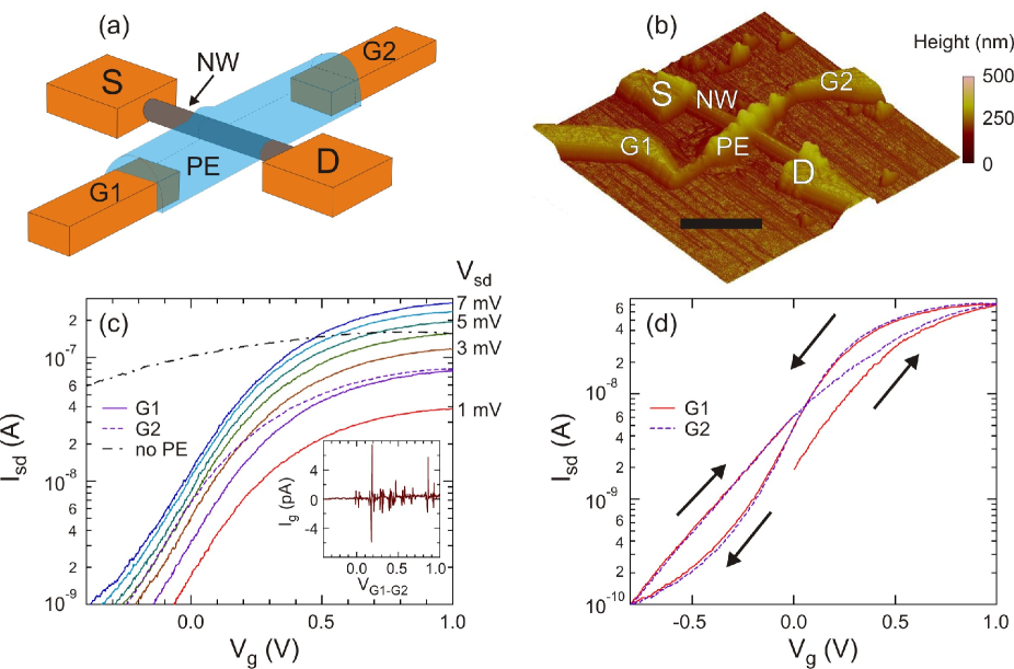
Figures 2(a/b) show a nanowire transistor incorporating a single polymer electrolyte gate (PE) connected to two Ni/Au gate electrodes (G1 and G2). The second electrode was used to test whether the electrode-nanowire separation, or , influences PE gate operation; electrodes G1 and G2 are separated from the nanowire by m (fixed) and m (varied between devices), respectively. The PE gate has a polymer:salt ratio of and was written with nm and C/m2, giving a strip with nm and nm. Figure 2(c) shows the source-drain current versus PE gate voltage for seven different source-drain biases between and mV with applied to G1 (solid lines) and at mV with applied to G2 (dashed line). In all experiments, the electrode that did not have applied was kept at ground - however there was no major difference to the transfer characteristics if this electrode was floated (see Supplementary Figure S2(a)). There is hysteresis in the gate characteristics, as we show in Fig. 2(d) and discuss further below. Hence for the data in Fig 2(c) we only show data obtained for one sweep direction: from positive towards more negative . Considering data for applied to G1 first, we obtain a subthreshold swing of mV/decade for data in Fig. 2(c). Across devices studied so far with polymer:salt ratio (a total of working gates) we obtain an average subthreshold swing mV/decade. The average threshold voltage was V at mV across the devices. We now look at the influence of the separation between the gate electrode and the nanowire on the transistor characteristics. For the device measured in Fig .2(d), m and m. Despite this difference, the gate characteristics in Fig. 2(c) are very similar with almost identical subthreshold swing. We find this same behaviour across many devices where ranges from m to m (see Supplementary Figure S2(b)). The lack of dependence of the sub-threshold swing on gate electrode to nanowire separation is not surprising; for an ideal EDL, drops across the nanowire/electrolyte and electrode/electrolyte interfaces, not across the electrolyte itself. The result is that the steady state gate capacitance – and thereby the subthreshold swing – is independent of the electrode-nanowire separation. Note that the polymer electrolyte is not electronically conductive; Fig. 2(c) (inset) shows a plot of current through the PE gate versus potential difference between electrodes G1 and G2 demonstrating a negligible electronic conductivity despite a significant ionic conductivity.
Gate hysteresis is a common issue for transistors incorporating polymer electrolyte gate dielectrics. It normally arises due to the finite ionic mobility of the polymer electrolyte, since ions need to drift through the polymer to re-establish electrostatic equilibrium at the EDLs when the voltage on the gate electrode is altered. This hysteresis will depend on properties of the polymer electrolyte, but also on the distance between the gate electrode and transistor channel. On its own, the delay imposed by ion migration means that for sweeps from positive (negative) to negative (positive) gate voltages will be higher (lower) than otherwise expected, producing a counter-clockwise hysteresis loop. Figure 2(d) shows extended vs traces for G1 (solid red line) and G2 (dashed purple line) for a device with m and m. Two interesting features are evident. First, neither gate trace follows a simple, counter-clockwise cyclical loop; instead they take a ‘figure of 8’ form that indicates possible additional contributions to the hysteresis. One additional contribution may be charge trapping by nanowire surface states32, 18, which would depend on the exact nature of the InAs/PEO interface. Second, aside from the ‘virgin’ behavior in the initial positive ramp of G1, the hysteresis traces for G1 and G2 are identical, despite the factor of 4 difference between and . While the gate response is not identical for all devices, there is no clear relation between the magnitude of the hysteresis and . This also points to contributions other than ionic mobility to the hysteresis, and suggests that these other contributions are dominant. Indeed, much smaller hysteresis loops are typically seen in organic transistor and carbon nanotube devices with PEO/\ceLiClO4 gate dielectrics10, 33. We characterise the hysteresis further in the Supplementary Information, but most notably, the hysteresis can be reduced significantly by sweeping over a smaller gate range and/or at a lower rate. Determining the relative contributions of ionic mobility, surface states and other possible contributions to the gate hysteresis is beyond the scope of this work, but would be an interesting subject for future studies.
We now consider the effect of increased salt content on the device structure in Fig. 2(a/b). The first place where this presents an effect is in device fabrication. Unlike the test structures in Fig. 1, here we need to precisely align the PE gate to the gate electrodes and nanowire, and this is done by briefly viewing metal alignment markers on the substrate immediately prior to EBL patterning to ensure correct pattern alignment. Increasing the polymer:salt ratio to makes the PEO/\ceLiClO4 film opaque to the electron beam, resulting in difficulties in pattern alignment and thereby dramatically reducing device yield. Interestingly, increasing the polymer:salt ratio to returns some of the PEO/\ceLiClO4 film’s transparency to an electron beam – we explain this below. The second place where we see a salt concentration effect is in the electrical characteristics. Despite reduced yield, we successfully measured four devices at obtaining an average subthreshold swing of mV/decade from eight gates, and four devices at obtaining an average subthreshold swing of mV/decade from eight gates measured. Both the maximal electron beam opacity of the PEO/\ceLiCLO4 film and maximal subthreshold swing at intermediate polymer:salt ratio can be explained by the ‘ionic conductivity peak’ observed as a function of salt concentration; 34 this peak typically occurs at . 35 Thus we have concluded that a polymer:salt ratio offers the best compromise between patternability and device performance for the remainder of this work.
Comparing the performance of our PE gated devices to other nanowire transistors, our typical subthreshold swing of mV/decade compares very favorably with substrate-gated nanowire transistors, where subthreshold swings of order V/decade are typical. 15 The performance is also competitive with metal/oxide wrap-gated nanowire transistors, where subthreshold swings typically range from 100 to 750 mV/decade. 15, 36, 37, 38, 18, 39 This is particularly impressive as the polymer electrolyte does not completely wrap around the nanowire in our devices, unlike in Ref. 11 where a HF etch was used to ‘undercut’ the nanowire to provide access for the PEO/\ceLiClO4 film. This undercut etch was impractical to implement here as our \ceHfO2 cap layer is much more resistant to HF etching than \ceSiO2; 15 this step could easily be implemented for substrates with a thermally grown \ceSiO2 layer alone.
A concern that could be raised is that closely positioned, biased metal electrodes can also influence nanowire conduction. 40 Since we observed evidence for some electron capture by \ceLi+ ions at the patterning stage, the question that naturally follows is: To what extent does the direct coupling of the metal electrodes to the nanowire contribute to modulation of with ? For example, is it that \ceLi+ ions are neutralized by incident electrons during EBL such that ionic conduction is a co-contributor with electrostatic repulsion via the gate electrodes, rather than the dominant contributor to channel depletion? The black dot-dash trace in Fig. 2(c) shows the characteristics for a device like that in Fig. 2(a/b), but without any PEO/\ceLiClO4. At V the bare electrode has only reduced by a factor of compared to factor of for the PE-gated device. Pinch-off can be achieved with a bare electrode, but it requires V with m and a much more negative at greater electrode-nanowire separations. This is expected, since there is no EDL formation for bare electrode gating. The behavior of the bare electrode suggests that EDL formation is the dominant contributor to channel depletion in devices with a polymer electrolyte, despite any ionic mobility loss or neutralization that may arise from the EBL process. We confirm this via one final test with our dual PE-gated devices, which we now discuss.
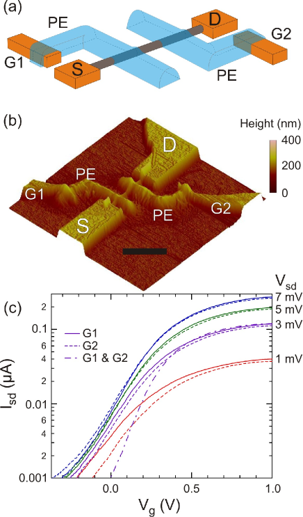
Figures 3(a/b) show a PE-gated device with two independent gates. Here, we have located the electrodes G1 and G2 such that their direct electrostatic coupling to the nanowire is screened by the source/drain contacts. This ensures that all depletion in this device arises from EDL formation by ion migration in the polymer electrolyte, which had polymer:salt ratio . Figure 3(c) shows versus for G1 with G2 grounded (solid lines) and G2 with G1 grounded (dashed lines) for several different . The characteristics for the two gates are similar, with G1 and G2 giving subthreshold swings of and mV/decade, respectively. These values are within error for the average values obtained from the single gate devices; this demonstrates that direct coupling to the metal electrodes makes a negligible contribution to depletion and that consistent performance can be obtained from our PE gate structures. The dotted line in Fig. 3(c) shows the characteristics obtained when is applied to both G1 and G2 simultaneously. The subthreshold swing improves to mV/decade, suggesting that performance gains might be achieved in our single PE-gate transistors by careful adjustment of gate width.
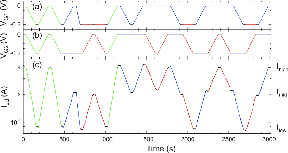
To better assess the control, balance and temporal stability of these gates, and gauge the potential for making more complex devices, e.g., a single electron transistor, we performed a more in-depth study of the two gates in our dual PE-gate transistor device when used within an operating range with relatively low hysteresis. This involved taking the device in Fig. 3(b) through a ‘program’ where G1 and G2 were swept together or separately between two pre-defined voltages mV and V. The program for G1 and G2 versus time is shown in Figs. 4(a) and (b), respectively, with the response plotted in Fig. 4(c). The full program takes 50 min, and the program is paused after each gate sweep to check stability for 30 s (black segments). The program produces an that alternates between three distinct current states , and , which correspond to three gate configurations: = = ; = , = or = , = , and = = . The fact that for both , and , highlights the strong electrical balance between the two nominally identical patterned PE gates. Further, the consistent return to , and across the program in Fig. 4 demonstrates the stability and low gate drift of this device within this operating region.
One could equally view Fig. 4 as a demonstration of two-gate logic, where we set input states [1, 1] (), [1, 0] (, ), [0, 1] (, ) and [0, 0] () giving either AND or OR operations as output if the threshold is set above or below , respectively. While logic is in principle possible in this device, the time response of the polymer electrolyte gates is insufficient to be competitive for applications. The data in Fig. 4 represents the fastest operation we can presently achieve, i.e., a few mV/s, without compromising on stability and reproducibility in of the logic states. For faster sweeps, the current at each state is less stable over the 30 s period and the value of the current at each state varies throughout the program. This makes each state less distinct and limits the practical switching speed to less than 1 Hz. There is some scope for improving the switching speed in future work by passivation of surface states, or engineering of the polymer electrolyte, e.g. by optimizing PEO/\ceLiClO4 salt content or adding plasticisers/nanoparticles. 41, 42, 43 While switching speeds from Hz have been obtained in solid polymer electrolytes such as PEO/\ceLiClO4, speeds up to kHz can be obtained by moving to a special class of polymer electrolytes known as ‘ion gels’. 44, 45, 1, 23, 46 These consist of an ionic liquid, i.e., a room-temperature molten salt, dispersed in a gel matrix typically formed using a block copolymer. A common example is 1-ethyl-3-methylimidazolium bis(trifluoromethylsulfonyl)imide ([EMIM][TFSI]) in poly(styrene - block - ethylene oxide - block - styrene). 23 A first step may be to attempt EBL patterning of PEO-containing ion gels; 46, 24, 44 however, it is possible these would suffer the same resolution difficulties described above. Another candidate may be PMMA-based ion gels: 23, 45 PMMA is a high resolution negative-tone resist under very high electron doses, with feature sizes as small as nm reported 47. This could potentially solve both the resolution and switching speed problems encountered here, and lead to nanoscale electrolyte gates with high resolution, ionic conductivity and switching speed. Nevertheless, the patterned PEO/\ceLiClO4 polymer electrolyte is an effective gate dielectric for applications where a strong field is required but fast switching speeds are not.
In conclusion, we have demonstrated electron-beam patterning of PEO/\ceLiClO4 electrolyte that allows gating of individual InAs nanowires with single or multiple independently controllable gates without gate/contact overlap. The electrolyte facilitates strong gate-channel coupling; the subthreshold swing of our devices is comparable to that of wrap-gated devices and tends to improve with greater channel coverage. The fabrication of these devices is simpler than for wrap-gated devices: only one extra EBL step is required compared to traditional substrate-gated nanowire transistors. Our dual PE-gated devices exhibit independent gate control and ability to perform basic logic operations.
Materials and methods.
Fabrication Nanowire devices were fabricated from 3 - 6 m long, 50 nm diameter InAs nanowires grown by MOCVD. Devices were fabricated on .cm As-doped Si wafer (Silicon Valley Microelectronics) with a nm thermal oxide and an additional nm \ceHfO2 layer deposited by atomic layer deposition. This wafer was prepatterned with Ti/Au interconnects and EBL alignment structures before being divided into smaller ‘chips’ on which nanowire transistors were made. Nanowires were deposited by dry transfer using lab wipe. Source, drain and gate electrodes were then defined by EBL using a Raith 150-two system. The EBL resist was a solution of k MW PMMA in anisole (Microchem) deposited by spin coating at rpm followed by a min hotplate bake at C, developed using a mixture of methylisobutylketone in 2-propanol. The electrodes consisted of 25 nm Ni and 75 nm Au deposited by thermal evaporation, immediately after a 120 s (NH4)2Sx contact passivation step at C.48 Lift-off was performed overnight in N-methyl-2-pyrrolidone at C. Following lift-off, a PEO/\ceLiClO4 film was spin-coated, baked and patterned by EBL as described in the main text to produce completed devices, which were then packaged in LCC20 ceramic chip carriers (Spectrum) and bonded using an Au ball bonder (Kulicke & Soffa 4500). Atomic Force Microscopy (AFM) studies were performed prior to packaging using a Dimension DI-3000 AFM in tapping mode using Veeco OTESPA7 probes. AFM was performed in cleanroom ambient atmosphere (temperature C and relative humidity ).
Electrical Characterization
All electrical characterization presented here was performed at room temperature and atmosphere. The source-drain current was measured using a Stanford Research Systems SRS830 lock-in amplifier with an a.c. excitation mV applied at a frequency of Hz using the internal oscillator. Gate electrodes were biased to using Yokogawa GS200 or Keithley 2400 voltage sources with built-in current monitoring for tracking the gate leakage current. The gate current in the inset of Fig. 2(c) was monitored by a Keithley 6517A electrometer.
Devices were stored in the dark in vacuum between measurements to preserve the quality of the ohmic contacts 48 and polymer electrolytes. Under these conditions, device characteristics typically remained reproducible for a period of 3 - 4 months before beginning to degrade (see Supplementary Figure S4).
Supporting Information. Additional supporting data on line-width studies as well as device characteristics, hysteresis and longevity. This material is available free of charge via the Internet at http://pubs.acs.org.
Corresponding author. *E-mail: adam.micolich@nanoelectronics.physics.unsw.edu.au
This work was funded by the Australian Research Council (ARC), Nanometre Structure Consortium @ Lund University (nmC@LU), Swedish Research Council (VR), and Knut and Alice Wallenberg Foundation (KAW) APM acknowledges an ARC Future Fellowship (FT0990285). We thank D. Liang and X.P.A. Gao for helpful discussions, and D. Alvares, P.-H. Prevot and F. Ladouceur for assistance with initial polymer electrolyte development. This work was performed in part using the NSW and ACT nodes of the Australian National Fabrication Facility (ANFF).
References
- Kim et al. 2013 Kim, S. H.; Hong, K.; Xie, W.; Lee, K. H.; Zhang, S.; Lodge, T. P.; Frisbie, C. D. Advanced Materials 2013, 25, 1822–1846
- Samuelson 2003 Samuelson, L. Materials today 2003, 6, 22 – 31
- Thelander et al. 2006 Thelander, C.; Agarwal, P.; Brongersma, S.; Eymery, J.; Feiner, L. F.; Forchel, A.; Scheffler, M.; Riess, W.; Ohlsson, B. J.; Gösele, U.; Samuelson, L. Materials today 2006, 9, 28 – 35
- Armand 1986 Armand, M. B. Annual Review of Materials Science 1986, 16, 245–261
- Takeya et al. 2006 Takeya, J.; Yamada, K.; Hara, K.; Shigeto, K.; Tsukagoshi, K.; Ikehata, S.; Aoyagi, Y. Applied Physics Letters 2006, 88, 112102
- Panzer et al. 2005 Panzer, M. J.; Newman, C. R.; Frisbie, C. D. Applied Physics Letters 2005, 86, 103503
- Panzer and Frisbie 2006 Panzer, M. J.; Frisbie, C. D. Advanced Functional Materials 2006, 16, 1051–1056
- Rosenblatt et al. 2002 Rosenblatt, S.; Yaish, Y.; Park, J.; Gore, J.; Sazonova, V.; McEuen, P. L. Nano Letters 2002, 2, 869–872
- Siddons et al. 2004 Siddons, G. P.; Merchin, D.; Back, J. H.; Jeong, J. K.; Shim, M. Nano Letters 2004, 4, 927–931
- Ozel et al. 2005 Ozel, T.; Gaur, A.; Rogers, J. A.; Shim, M. Nano Letters 2005, 5, 905–911
- Liang and Gao 2012 Liang, D.; Gao, X. P. A. Nano Letters 2012, 12, 3263–3267
- Duan et al. 2001 Duan, X.; Huang, Y.; Cui, Y.; Wang, J.; Lieber, C. M. Nature 2001, 409, 66–69
- Fasth et al. 2005 Fasth, C.; Fuhrer, A.; Björk, M. T.; Samuelson, L. Nano Letters 2005, 5, 1487–1490
- Pfund et al. 2006 Pfund, A.; Shorubalko, I.; Leturcq, R.; Ensslin, K. Applied Physics Letters 2006, 89, 252106
- Storm et al. 2012 Storm, K.; Nylund, G.; Samuelson, L.; Micolich, A. P. Nano Letters 2012, 12, 1–6
- Dhara et al. 2011 Dhara, S.; Sengupta, S.; Solanki, H. S.; Maurya, A.; Pavan R., A.; Gokhale, M. R.; Bhattacharya, A.; Deshmukh, M. M. Applied Physics Letters 2011, 99, 173101–173103
- Khanal and Wu 2007 Khanal, D. R.; Wu, J. Nano Letters 2007, 7, 2778–2783
- Thelander et al. 2008 Thelander, C.; Rehnstedt, C.; Fröberg, L. E.; Lind, E.; Martensson, T.; Caroff, P.; Lowgren, T.; Ohlsson, B. J.; Samuelson, L.; Wernersson, L.-E. IEEE Transactions on Electron Devices 2008, 55, 3030–3036
- Ford et al. 2012 Ford, A. C.; Kumar, S. B.; Kapadia, R.; Guo, J.; Javey, A. Nano Letters 2012, 12, 1340–1343
- Tian et al. 2012 Tian, Y.; Sakr, M. R.; Kinder, J. M.; Liang, D.; MacDonald, M. J.; Qiu, R. L. J.; Gao, H.-J.; Gao, X. P. A. Nano Letters 2012, 12, 6492–6497
- van Weperen et al. 2013 van Weperen, I.; Plissard, S. R.; Bakkers, E. P. A. M.; Frolov, S. M.; Kouwenhoven, L. P. Nano Letters 2013, 13, 387–391
- de Gans et al. 2004 de Gans, B.-J.; Duineveld, P. C.; Schubert, U. S. Advanced Materials 2004, 16, 203–213
- Cho et al. 2008 Cho, J. H.; Lee, J.; Xia, Y.; Kim, B.; He, Y.; Renn, M. J.; Lodge, T. P.; Frisbie, C. D. Nature Materials 2008, 7, 900–906
- Choi et al. 2010 Choi, J.-H.; Lee, S. W.; Kar, J. P.; Das, S. N.; Jeon, J.; Moon, K.-J.; Lee, T. I.; Jeong, U.; Myoung, J.-M. Journal of Materials Chemistry 2010, 20, 7393–7397
- Krsko et al. 2003 Krsko, P.; Sukhishvili, S.; Mansfield, M.; Clancy, R.; Libera, M. Langmuir 2003, 19, 5618–5625
- Hong et al. 2004 Hong, Y.; Krsko, P.; Libera, M. Langmuir 2004, 20, 11123–11126
- Uchiyama et al. 2009 Uchiyama, R.; Kusagawa, K.; Hanai, K.; Imanishi, N.; Hirano, A.; Takeda, Y. Solid State Ionics 2009, 180, 205–211
- Ueno et al. 2011 Ueno, M.; Imanishi, N.; Hanai, K.; Kobayashi, T.; Hirano, A.; Yamamoto, O.; Takeda, Y. Journal of Power Sources 2011, 196, 4756–4761
- Murata et al. 1981 Murata, K.; Kyser, D. F.; Ting, C. H. Journal of Applied Physics 1981, 52, 4396–4405
- Shimizu and Ze-Jun 1992 Shimizu, R.; Ze-Jun, D. Reports on Progress in Physics 1992, 55, 487–531
- Aizaki 1979 Aizaki, N. Journal of Vacuum Science and Technology 1979, 16, 1726–1733
- Lind et al. 2006 Lind, E.; Persson, A. I.; Samuelson, L.; Wernersson, L.-E. Nano Letters 2006, 6, 1842–1846
- Panzer and Frisbie 2006 Panzer, M. J.; Frisbie, C. D. Applied Physics Letters 2006, 88, 203504–203506
- Bruce and Vincent 1993 Bruce, P. G.; Vincent, C. A. J. Chem. Soc., Faraday Trans. 1993, 89, 3187 – 3203
- Fullerton-Shirey and Maranas 2009 Fullerton-Shirey, S. K.; Maranas, J. K. Macromolecules 2009, 42, 2142–2156
- Rehnstedt et al. 2008 Rehnstedt, C.; Martensson, T.; Thelander, C.; Samuelson, L.; Wernersson, L.-E. IEEE Transactions on Electron Devices 2008, 55, 3037–3041
- Fröberg et al. 2008 Fröberg, L. E.; Rehnstedt, C.; Thelander, C.; Lind, E.; Wernersson, L.; Samuelson, L. IEEE Electron Device Letters 2008, 29, 981–983
- Rehnstedt et al. 2008 Rehnstedt, C.; Thelander, C.; Fröberg, L. E.; Ohlsson, B. J.; Samuelson, L.; Wernersson, L.-E. Electronics Letters 2008, 44, 236
- Tanaka et al. 2010 Tanaka, T.; Tomioka, K.; Hara, S.; Motohisa, J.; Sano, E.; Fukui, T. Applied Physics Express 2010, 3, 025003
- Roddaro et al. 2011 Roddaro, S.; Pescaglini, A.; Ercolani, D.; Sorba, L.; Beltram, F. Nano Letters 2011, 11, 1695–1699
- Croce et al. 1998 Croce, F.; Appetecchi, G. B.; Persi, L.; Scrosati, B. Nature 1998, 394, 456
- Qian et al. 2001 Qian, X.; Gu, N.; Cheng, Z.; Yang, X.; Wang, E.; Dong, S. Journal of Solid State Electrochemistry 2001, 6, 8–15
- Wang et al. 2005 Wang, G. X.; Yang, L.; Wang, J. Z.; Liu, H. K.; Dou, S. X. Journal of Nanoscience and Nanotechnology 2005, 5, 1135–1140
- Klingshirn et al. 2004 Klingshirn, M. A.; Spear, S. K.; Subramanian, R.; Holbrey, J. D.; Huddleston, J. G.; Rogers, R. D. Chemistry of Materials 2004, 16, 3091–3097
- Susan et al. 2005 Susan, M. A. B. H.; Kaneko, T.; Noda, A.; Watanabe, M. Journal of the American Chemical Society 2005, 127, 4976–4983
- Lee et al. 2007 Lee, J.; Panzer, M. J.; He, Y.; Lodge, T. P.; Frisbie, C. D. Journal of the American Chemical Society 2007, 129, 4532–4533
- Zailer et al. 1996 Zailer, I.; Frost, J. E. F.; Chabasseur-Molyneux, V.; Ford, C. J. B.; Pepper, M. Semiconductor Science and Technology 1996, 11, 1235–1238
- Suyatin et al. 2007 Suyatin, D. B.; Thelander, C.; Björk, M. T.; Maximov, I.; Samuelson, L. Nanotechnology 2007, 18, 105307