Effect of Point Defects on the Optical and Transport Properties of MoS2 and WS2
Abstract
Imperfections in the crystal structure, such as point defects, can strongly modify the optical and transport properties of materials. Here, we study the effect of point defects on the optical and DC conductivities of single layers of semiconducting transition metal dichalcogenides with the form S2, where =Mo or W. The electronic structure is considered within a six bands tight-binding model, which accounts for the relevant combination of orbitals of the metal and orbitals of the chalcogen . We use the Kubo formula for the calculation of the conductivity in samples with different distributions of disorder. We find that and/or S defects create mid-gap states that localize charge carriers around the defects and which modify the optical and transport properties of the material, in agreement with recent experiments. Furthermore, our results indicate a much higher mobility for -doped WS2 in comparison to MoS2.
Introduction— The mobility of current single layer crystals of transition metal dichalcogenides (TMD) is highly dependent on the screening environment and is limited by the presence of defects in the samples. The existence of defects in the chemical and structural composition of those materials can influence their optical and transport properties, as revealed by recent experimental results. A broad peak at nm ( eV) in the optical spectrum of bilayer MoS2 has been associated to impurities Wu et al. (2013) whereas the mobility of multilayer samples has been shown to highly depend on the substrate and dielectric effects Bao et al. (2013). Vacancy defects in the crystal, which can be created by means of thermal annealing and -particle Tongay et al. (2013) or electron beam irradiation Zhou et al. (2013a); Qiu et al. (2013), trap free charge carriers and localize excitons, leading to new peaks in the photoluminescence spectra Tongay et al. (2013). Recent experiments Qiu et al. (2013) show that the density of sulphur vacancies in MoS2 is of the order of cm-2, corresponding to an average defect distance about 1.7 nm. The existence of line defects, which separate patches or islands where the layer direction is opposite to its surrounding, can lead to changes in the carrier mobility Enyashin et al. (2013), and the importance of short-range disorder has been proposed as the main limitation for the mobility of chemical vapor deposition (CVD) grown single-layer MoS2 Zhu et al. (2014); Schmidt et al. (2014).
Therefore, it is necessary to understand the effect of impurities in the optical and transport properties of TMD, as a first step to exploit the controlled creation of defects as a route to manipulate their electronic properties. There are several theoretical works which have studied this problem using ab initio methods Ataca and Ciraci (2011); Ma et al. (2011); Wei et al. (2012); Komsa et al. (2012); Ghorbani-Asl et al. (2013); Zhou et al. (2013b); Enyashin et al. (2013); Liu et al. (2013). However, the simulation of realistic disordered samples of TMD with a random distribution of defects are extremely expensive computationally for density functional theory (DFT) methods, since they require a very large unit cell in the calculation. In this paper we follow an alternative route and perform a systematic study of the density of states, optical and DC conductivities of single-layers of MoS2 and WS2 in the presence of point defects, by means of a real space tight-binding (TB) model for large systems, containing millions of atoms. In our simulations, Mo/W and S point defects are introduced by elimination of atoms which are randomly distributed over the sample. This method allows us to study point defects such as unreconstruced vacancies, chemically bonded atoms or molecules, and strong substitutional defects which prevent the electronic hopping to the neighbors. We also consider clusters of point defects. We use a TB model that considers the relevant orbital contribution in the valence and conduction bands, as well as the effect of spin-orbit coupling (SOC) Cappelluti et al. (2013); Roldán et al. (2014). The optical and electronic properties are obtained numerically by using the tight-binding propagation methods (TBPM) Yuan et al. (2010); Wehling et al. (2010); Yuan et al. (2011, 2012). Our results show that point defects create midgap states whose energy depends on the specific impurities. We show that optical transitions involving the impurity bands lead to a background contribution in the photoconductivity at low energies, in agreement with recent experiments Mak et al. (2010). We further calculate the DC conductivity of disordered MoS2 and WS2, finding that the impurity states do not contribute to the conductivity within the gap, whereas they lead to a depletion of it outside the gap.

Method— Transition metal dichalcogenides as MoS2 and WS2 are composed, in its bulk configuration, of two-dimensional S--S layers (Mo,W) stacked on top of each other, coupled by weak van der Waals forces. The transition metal atoms are ordered in a triangular lattice, each of them bonded to six S atoms located in the top and bottom layers, forming a sandwiched material. Similarly as in graphene, the weak interlayer coupling makes possible to exfoliate this material down to a single-layer Novoselov et al. (2005). The electronic band structure of MoS2 changes from an indirect band gap for multilayer samples, to a direct gap semiconductor for single-layers Splendiani et al. (2010); Cappelluti et al. (2013). We consider a 6-bands tight-binding model which contains the proper orbital combination that contributes to the valence and conduction bands of S2: 3 -orbitals of the transition metal (, and ) as well as the symmetric (antisymmetric) combination of the () orbitals of the top and bottom chalcogen atoms Cappelluti et al. (2013); Castellanos-Gomez et al. (2013). The base vector can be written as
| (1) |
where , , and the subscripts and refer to the top and bottom S layers, respectively.
We also consider the intra-atomic spin-orbit coupling , where S accounts for both, the transition metal as well as the chalcogen atom S, is the corresponding intra-atomic SO interaction, is the atomic angular momentum operator, and is the spin operator. The optical and electronic properties, such as density of states (DOS), quasi-eigenstates, optical and DC conductivities, are obtained numerically by using the TBPM Yuan et al. (2010); Wehling et al. (2010); Yuan et al. (2011, 2012) (more details can be found in the Supplementary Material).
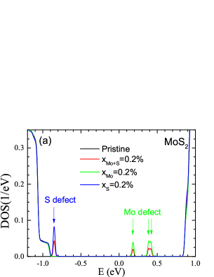
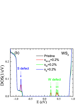
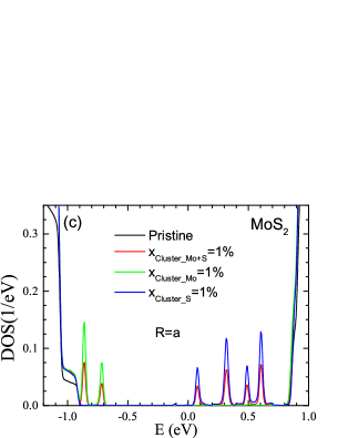
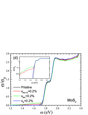
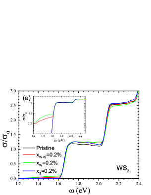
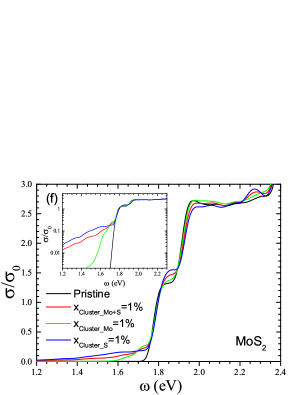
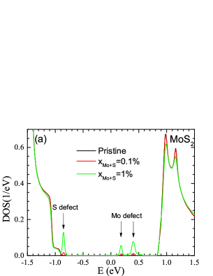
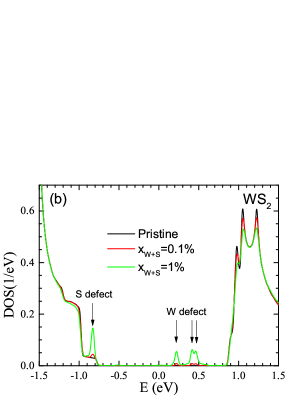
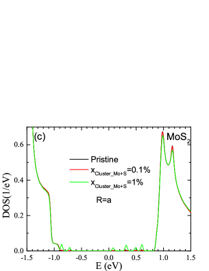
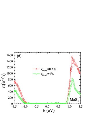
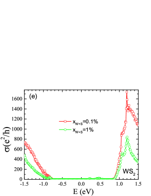
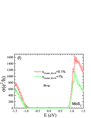
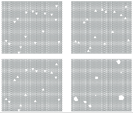
Results and discussion— The effect of point defects in the DOS of MoS2 and WS2 are shown in Fig. 1(a)-(c). The defect concentration for single point defects in Fig. 1(a) and (b) is chosen to be of the same order as the intrinsic vacancies observed in recent experiments Qiu et al. (2013). For clean samples (black lines), the DOS has a gap which corresponds to the well known direct gap of single layer samples at the points of the Brillouin zone (BZ). Defects in the samples lead to the appearance of a series of peaks in the gapped region of the DOS, which are associated to the creation of midgap states localized around the defects, whose energy and strength depends on the specific missing atoms, their concentration as well as the specific arrangement of the point defects as individual missing atoms [Fig. 1(a) and (b)] or in clusters of point defects with variable radius [Fig. 1(c)]. For the same concentration of defects, isolated point defects modify more strongly the DOS than clusters of defects. This is the reason why we show results for 0.2% of single defects, and 1% of cluster of defects with a radius 111See Supplementary Material for a detailed description of the arrangement of the defects in our calculation.. The impurity states have also an important effect on the optical conductivity [Fig. 1(d)-(e)]. First, let us consider the case of undoped and clean MoS2 and WS2. Since single layers of those TMD are direct gap semiconductors, the only optical transitions allowed at low energies are two set of inter-band transitions with from the edges of the SOC split valence bands to the conduction band at the and points of the BZ Li and Carbotte (2012). Those transitions lead to the A and B absorption peaks observed in photoluminescence experiments Mak et al. (2010), and the SOC splitting of the valence band manifests itself in the optical conductivity through the step like feature of that can be seen in the black lines (for pristine MoS2 and WS2) of Fig. 1(d)-(f). This feature is especially visible for WS2 due to the strong SOC associated to the heavy W atom Roldán et al. (2014), which lead to a plateau like feature for of meV, in agreement with the energy separation between the spin polarized valence bands. The existence of defects in the sample lead to flat midgap bands which activate new optical transitions with in the optical spectrum. Most importantly, these new optical transitions lead to a background contribution which appears in the optical conductivity at low energies, as it can be seen in Fig. 1(d)-(f) for different concentration of defects, suggesting that resonant impurities, like the defects studied in this work, could have a relevant contribution to the optical spectrum of TMDs Mak et al. (2010). Furthermore, it is interesting to note that this background contribution due to disorder resembles that observed in the the optical conductivity of highly doped graphene Li et al. (2008).
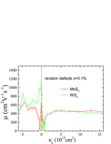
Our results for the DC conductivities are shown in Fig. 2, which demonstrate a significant asymmetry between electrons and holes, in reasonable agreement with experiments Bao et al. (2013) (note that the observations are done in multilayered samples). The fact that Mo and W defects lead to localized states well inside the gap, as illustrated by the densities of states also shown in Fig. 2, combined with the fact that the bands at the and points of the BZ can be approximated by an effective gapped Dirac equation Xiao et al. (2012); Lu et al. (2013), suggests that these defects can act as resonant scatterers Stauber et al. (2007), which give rise to a mobility almost independent of the carrier density (see below and the T-matrix analysis in the Supplementary Material).
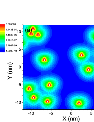
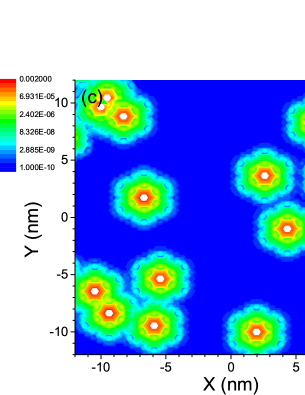
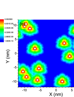
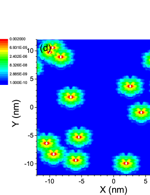
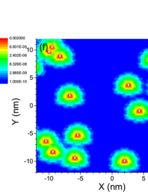
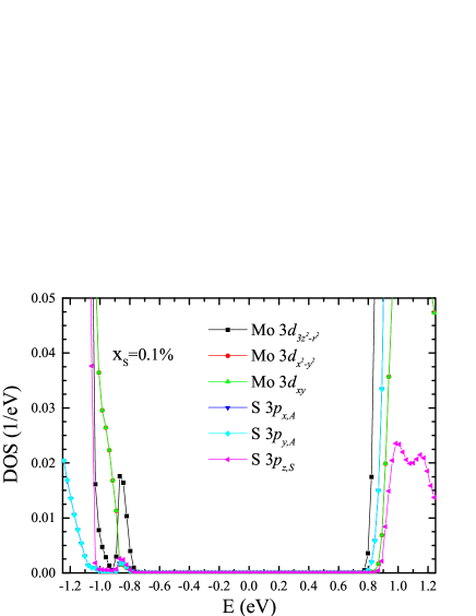
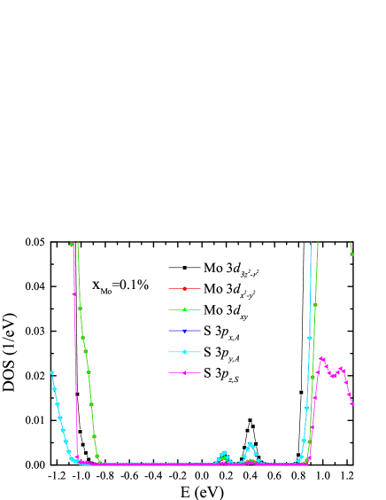
The localization of these midgap states are clearly seen by their local density of states (LDOS) plotted in Fig. 3. The amplitude of each orbital in real space is obtained from the average of quasiegenstates with different initial states. The profiles of the localized states show either hexagonal symmetry or mirror symmetry, depending on the type of the orbital and the energy of the midgap states. For S defects, the impurity state at the energy eV is localized mainly () on orbitials of neighboring Mo atoms, with small amount () on orbitals of neighboring S atoms. For Mo defects, on the other hand, there are two midgap states, one centered at eV, with mainly localized and orbitals, and another centered at eV, with mainly localized and orbitals. The detailed DOS of each orbital as a function of energy is shown in the Supplementary Material.
Results for the carrier mobility, defined as , where the charge density is obtained from the integral of density of states via are shown in Fig. 4. We notice that -doping corresponds to Mo(W) point defects, whereas -doping corresponds to S point defects. We observe that for -doped samples, MoS2 and WS2 show similar mobilities, whereas for -doped samples, the mobility of WS2 is larger than for MoS2. Our results show that in general, the mobilities of TMDs are low, but they are larger for holes than for electrons, in agreement with previous experimental results Bao et al. (2013); Zhu et al. (2014). The results for the mobility suggest that it is independent of carrier concentration, except at the edge of the valence band. As we have discussed before, this is consistent with the expected features of resonant scatterers. A more detailed analysis of resonant scatterers in gapped Dirac systems is required in order to make this statement more quantitative, however. Note, finally, that our analysis leaves out the effect of the missing charge at the defect, which can lead to a long range potential, and to intravalley scattering Peres (2010).
Conclusions— We have studied the effect of point defects in the DOS, optical and DC conductivity of single layers of TMDs like MoS2 and WS2. The existence of point defects in the sample creates flat midgap bands which activate new optical transitions in the optical spectrum, leading to a background contribution which appears in the optical conductivity at low energies, in agreement with photoconductivity measurements. Our results show a significant asymmetry between electrons and holes. The DC conductivities and mobilities are larger for holes, in agreement with experiments, and we find higher mobilities for -doped WS2 than for MoS2. Mo and W defects induce localized states well inside the gap, suggesting a behavior similar to that of resonant scatterers in graphene.
Acknowledgments— We thank the European Union Seventh Framework Programme under grant agreement n604391 Graphene Flagship. The support by the Stichting Fundamenteel Onderzoek der Materie (FOM) and the Netherlands National Computing Facilities foundation (NCF) are acknowledged. S.Y. and M.I.K. thank financial support from the European Research Council Advanced Grant program (contract 338957). RR acknowledges financial support from the Juan de la Cierva Program (MEC, Spain). R.R. and F.G. thank financial support from MINECO, Spain, through Grant No. FIS2011-23713, and the European Research Council Advanced Grant program (contract 290846).
References
- Wu et al. (2013) S. Wu, J. S. Ross, G.-B. Liu, G. Aivazian, A. Jones, Z. Fei, W. Zhu, D. Xiao, W. Yao, D. Cobden, et al., Nature Physics (2013).
- Bao et al. (2013) W. Bao, X. Cai, D. Kim, K. Sridhara, and M. S. Fuhrer, Applied Physics Letters 102, 042104 (2013).
- Tongay et al. (2013) S. Tongay, J. Suh, C. Ataca, W. Fan, A. Luce, J. S. Kang, J. Liu, C. Ko, R. Raghunathanan, J. Zhou, et al., Scientific reports 3 (2013).
- Zhou et al. (2013a) W. Zhou, X. Zou, S. Najmaei, Z. Liu, Y. Shi, J. Kong, J. Lou, P. M. Ajayan, B. I. Yakobson, and J.-C. Idrobo, Nano Letters 13, 2615 (2013a).
- Qiu et al. (2013) H. Qiu, T. Xu, Z. Wang, W. Ren, H. Nan, Z. Ni, Q. Chen, S. Yuan, F. Miao, F. Song, et al., Nature Communications 4, 2642 (2013).
- Enyashin et al. (2013) A. N. Enyashin, M. Bar-Sadan, L. Houben, and G. Seifert, The Journal of Physical Chemistry C (2013).
- Zhu et al. (2014) W. Zhu, T. Low, Y.-H. Lee, H. Wang, D. B. Farmer, J. Kong, F. Xia, and P. Avouris, Nature Communications 5, 3087 (2014).
- Schmidt et al. (2014) H. Schmidt, S. Wang, L. Chu, M. Toh, R. Kumar, W. Zhao, A. H. Castro Neto, J. Martin, S. Adam, B. Oezyilmaz, et al., ArXiv e-prints (2014), eprint 1401.1063.
- Ataca and Ciraci (2011) C. Ataca and S. Ciraci, The Journal of Physical Chemistry C 115, 13303 (2011).
- Ma et al. (2011) Y. Ma, Y. Dai, M. Guo, C. Niu, J. Lu, and B. Huang, Physical Chemistry Chemical Physics 13, 15546 (2011).
- Wei et al. (2012) J.-w. Wei, Z.-w. Ma, H. Zeng, Z.-y. Wang, Q. Wei, and P. Peng, AIP Advances 2, 042141 (2012).
- Komsa et al. (2012) H.-P. Komsa, J. Kotakoski, S. Kurasch, O. Lehtinen, U. Kaiser, and A. V. Krasheninnikov, Phys. Rev. Lett. 109, 035503 (2012).
- Ghorbani-Asl et al. (2013) M. Ghorbani-Asl, A. N. Enyashin, A. Kuc, G. Seifert, and T. Heine, ArXiv e-prints (2013), eprint 1311.0474.
- Zhou et al. (2013b) Y. Zhou, P. Yang, H. Zu, F. Gao, and X. Zu, Phys. Chem. Chem. Phys. 15, 10385 (2013b).
- Liu et al. (2013) D. Liu, Y. Guo, L. Fang, and J. Eq:H0, Applied Physics Letters 103, 183113 (2013).
- Cappelluti et al. (2013) E. Cappelluti, R. Roldán, J. A. Silva-Guillén, P. Ordejón, and F. Guinea, Phys. Rev. B 88, 075409 (2013).
- Roldán et al. (2014) R. Roldán, M. P. López-Sancho, E. Cappelluti, J. A. Silva-Guillén, P. Ordejón, and F. Guinea, ArXiv e-prints (2014), eprint 1401.5009.
- Yuan et al. (2010) S. Yuan, H. De Raedt, and M. I. Katsnelson, Phys. Rev. B 82, 115448 (2010).
- Wehling et al. (2010) T. O. Wehling, S. Yuan, A. I. Lichtenstein, A. K. Geim, and M. I. Katsnelson, Phys. Rev. Lett. 105, 056802 (2010).
- Yuan et al. (2011) S. Yuan, R. Roldán, H. De Raedt, and M. I. Katsnelson, Phys. Rev. B 84, 195418 (2011).
- Yuan et al. (2012) S. Yuan, T. O. Wehling, A. I. Lichtenstein, and M. I. Katsnelson, Phys. Rev. Lett. 109, 156601 (2012).
- Mak et al. (2010) K. F. Mak, C. Lee, J. Hone, J. Shan, and T. F. Heinz, Phys. Rev. Lett. 105, 136805 (2010).
- Novoselov et al. (2005) K. S. Novoselov, D. Jiang, F. Schedin, T. J. Booth, V. V. Khotkevich, S. V. Morozov, and A. K. Geim, Proc. Natl. Acad. Sci. USA 102, 10451 (2005).
- Splendiani et al. (2010) A. Splendiani, L. Sun, Y. Zhang, T. Li, J. Kim, C. Y. Chim, and F. Wang, Nano Lett. 10, 1271 (2010).
- Castellanos-Gomez et al. (2013) A. Castellanos-Gomez, R. Roldán, E. Cappelluti, M. Buscema, F. Guinea, H. S. J. van der Zant, and G. A. Steele, Nano Letters 13, 5361 (2013).
- Li and Carbotte (2012) Z. Li and J. P. Carbotte, Phys. Rev. B 86, 205425 (2012).
- Li et al. (2008) Z. Li, E. A. Henriksen, Z. Jiang, Z. Hao, M. C. Martin, P. Kim, H. Stormer, and D. N. Basov, Nature Physics 4, 532 (2008).
- Xiao et al. (2012) D. Xiao, G.-B. Liu, W. Feng, X. Xu, and W. Yao, Phys. Rev. Lett. 108, 196802 (2012).
- Lu et al. (2013) H.-Z. Lu, W. Yao, D. Xiao, and S.-Q. Shen, Phys. Rev. Lett. 110, 016806 (2013).
- Stauber et al. (2007) T. Stauber, N. M. R. Peres, and F. Guinea, Phys. Rev. B 76, 205423 (2007).
- Peres (2010) N. M. R. Peres, Rev. Mod. Phys. 82, 2673 (2010).
- Hams and De Raedt (2000) A. Hams and H. De Raedt, Phys. Rev. E 62, 4365 (2000).
- Ishihara (1971) A. Ishihara, Statistical Physics (Academic Press, New York, 1971).
- Wehling et al. (2009) T. Wehling, M. Katsnelson, and A. Lichtenstein, Chemical Physics Letters 476, 125 (2009).
Supplementary Material
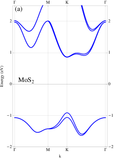
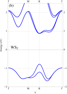
Tight-binding band structure and distribution of defects— In Fig. 5 we show the band structure of MoS2 and WS2 obtained from the TB model used in the calculations. The TB parameters are given in Ref. Roldán et al. (2014).
In Fig. 6 we show an sketch of the distribution of defects considered in the main text.
Tight-binding Propagation Method— Our method is based on the numerical solution of time-dependent Schödinger equation (TDSE) in the TB model. The initial state is considered as a random superposition of all orbitals over the whole space which covers all the energy eigenstates Hams and De Raedt (2000); Yuan et al. (2010)
| (2) |
where are random complex numbers normalized as , and represents the orbital with spin at site . The density of states can be obtained by the Fourier transformation of the overlap between the time-evolved state and the initial state as Hams and De Raedt (2000); Yuan et al. (2010)
| (3) |
Here we use units such that . The time-evolution operator is calcualted numerically by using Chebyshev polynomial algorithm, extremly efficient for a TB Hamitlonian which is a sparse matrix. Within the TBPM, the optical conductivity (omitting the Drude contribution at ) is calculated by using the Kubo formula Ishihara (1971); Yuan et al. (2010)
where is the inverse temperature, is the sample area, is the Fermi-Dirac distribution operator, and the time-dependent current operator in the ( or ) direction is .
The DC conductivity at zero temperature is calculated by using the Kubo formula at Ishihara (1971); Yuan et al. (2010)
where is the normalized quasi-eigensate 222 Following Ref. Yuan et al. (2010), the normalized quasi-eigenstate is defined from the quasi-eigenstate , which is a superposition of the degenerate eigenstates with the same eigenenergy , obtained as the Fourier transform of , i.e. The quasi-eigenstate is not exactly an energy eigenstate, unless the corresponding eigenstate is not degenerate at energy . The average of the real space distribution of the amplitude for different realization of intial states can be used to examine the localization of the modes Yuan et al. (2010, 2011, 2012). . The accuracy of TBPM is mainly determined by the time interval and total time steps used in the Fourier transformation. The main limitation of the numerical calculations is the size of the physical memory that can be used to store the quasi-eigenstates in the calculation of DC conductivity. In the present work, we have fixed the temperature to K for the optical conductivity and to for the DC conductivity. We study systems containing atoms, with periodic boundary conditions.
Orbital DOS— Here we complement the information for the localized states around the impurities shown in Fig. 3 of the main text, and we show in Fig. 7 the contribution of each orbital to the DOS of MoS2 with 0.1% of S or Mo defects.
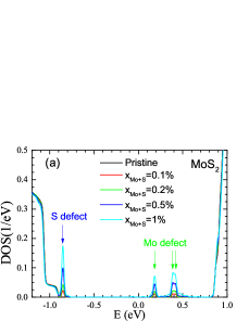
Dependence of the conductivity on the concentration of defects— In Fig. 8 we show results similar to Fig. 1 of the main text, but comparing different concentrations of defects. The height of the peaks in the DOS in the middle of the gap, associated to localized states around the impurities, increases with disorder, resulting in a larger background contribution to the optical conductivity for energies lower than the gap.
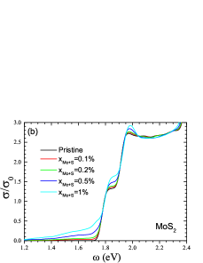
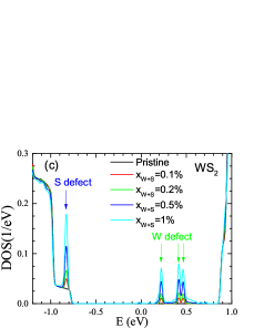
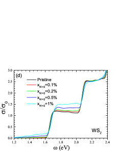
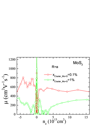
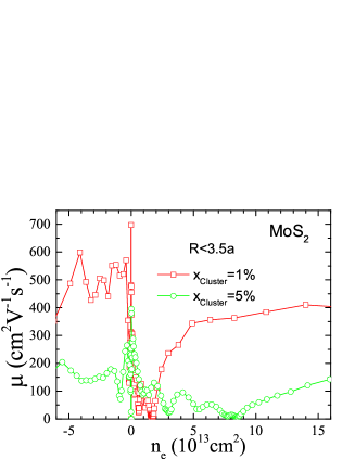
The mobility of the samples decreases with the concentration of defects, as it is shown in Fig. 9 for samples with clusters of defects, as stated in the figure.
Low energy model for the DC conductivity— The numerical results shown in Fig. 2 for the DC conductivity can be complemented with a low energy approximation in which we can calculate the conductivity using the matrix Wehling et al. (2009), which accounts for the scattering of electrons by resonant impurities
| (6) |
where is the potential accounting for the impurity, and is the local unperturbed Green’s function, which for a semiconductor with electron-hole asymmetry can be obtained from a density of states of the form , from which we obtain
| (7) |
where accounts for the width of the conduction (valence) bands. The case of interest here, which is defects, can be considered by the limit which leads to . From this the conductivity can be calculated from where is the scattering rate in terms of the concentration of impurities .
References
- Roldán et al. (2014) R. Roldán, M. P. López-Sancho, E. Cappelluti, J. A. Silva-Guillén, P. Ordejón, and F. Guinea, ArXiv e-prints (2014), eprint 1401.5009.
- Hams and De Raedt (2000) A. Hams and H. De Raedt, Phys. Rev. E 62, 4365 (2000).
- Yuan et al. (2010) S. Yuan, H. De Raedt, and M. I. Katsnelson, Phys. Rev. B 82, 115448 (2010).
- Ishihara (1971) A. Ishihara, Statistical Physics (Academic Press, New York, 1971).
- Wehling et al. (2009) T. Wehling, M. Katsnelson, and A. Lichtenstein, Chemical Physics Letters 476, 125 (2009).
- Yuan et al. (2011) S. Yuan, R. Roldán, H. De Raedt, and M. I. Katsnelson, Phys. Rev. B 84, 195418 (2011).
- Yuan et al. (2012) S. Yuan, T. O. Wehling, A. I. Lichtenstein, and M. I. Katsnelson, Phys. Rev. Lett. 109, 156601 (2012).