Integrated nanophotonics based on wire plasmons and atomically-thin material
Abstract
Photonic integrated circuits are an enabling technology in modern communications systems. The continually increasing demands for higher-speed and lower operating power devices have resulted in the continued impetus to shrink photonic components. In this work, we demonstrate a primitive nanophotonic integrated circuit element composed of a single silver nanowire and single-layer molybdenum disulfide (MoS2) flake. We show that nanowire plasmons can excite MoS2 photoluminescence via direct plasmon-to-exciton conversion along the wire and plasmon-to-photon-to-exciton conversion at the MoS2-covered wire end. We also find that the reverse process is possible: MoS2 excitons can decay into nanowire plasmons that can then be routed via the nanowire on-chip. Finally, we demonstrate that the nanowire may serve the dual purpose of both exciting MoS2 photoluminescence via plasmons and recollecting the decaying excitons.
1 Institute of Optics, University of Rochester, Rochester, New York 14627, USA
2Materials Science,University of Rochester, Rochester, New York 14627, USA
3ETH Zürich, Photonics Laboratory, 8093 Zürich, Switzerland
As silicon photonic integrated circuits have continued to mature1, novel nanophotonic devices and nanomaterials are being explored for their potential in next-generation on-chip optical processing2, 3. Particularly exciting is the possibility to engineer nanophotonic devices that both enhance light-matter interaction and support confined electromagnetic modes that can propagate in deeply subwavelength regions. Surface plasmon polaritons (SPPs)4, 5, electromagnetic excitations that propagate along the interface between a metal and a dielectric, are a natural candidate for both integrated subwavelength light guiding and pronounced light-matter coupling6, 7, 8, 9, 10, 11, 12. An exemplary system in this regard are silver (Ag) nanowires13, 14, 15, 16, 17, 18, 19, 20, 21, 22, 23 and, to date, the optical properties of individual Ag nanowires have been extensively studied19, 21, 23, 22, 20. A step towards efficient and compact nanophotonic circuitry is the integration of plasmonic waveguides that couple directly to on-chip sources, detectors, and modulators3. Initial steps have been made in coupling Ag nanowires with other nanostructures, such as quantum dots24, 25, 26, 27, fluorescent molecules28, and nitrogen-vacancy centers29, 30. Furthermore, near-field coupling between these nanostructures and the wire allows for plasmons to be generated anywhere along the wire, not just at the ends25, 27, 28, 29, 30. Recently, an on-chip germanium field-effect transistor has exploited this near-field coupling to directly measure Ag nanowire plasmons31.
Although there has been some investigation into graphene-nanowire hybrids for nanophotonic circuitry32, 33, the vast potential for two-dimensional atomically-thin materials in this realm is largely unexplored. Single-layer molybdenum disulfide (MoS2)34, a semiconductor being explored for its photoluminescence35, valley-selective properties36, 37, 38, and potential as a transistor39 and photodetector40, 41, is an ideal choice to couple with nanoplasmonic circuitry. In this paper, we explore the nanophotonics of a MoS2/Ag nanowire hybrid structure. We demonstrate coupling between a single-layer MoS2 flake and a single Ag nanowire. We show that a plasmon excited at the uncovered end of the nanowire can propagate and excite MoS2 photoluminescence (PL), both by direct plasmon-to-exciton conversion along the wire and by absorbing photons rescattering from the end of the wire. We also demonstrate MoS2 excitons can decay to generate Ag-nanowire plasmons. Finally, we show it is possible for the Ag nanowire to serve a dual role as both a channel for MoS2 excitation and subsequent extraction of the decaying MoS2 excitons.
Results
MoS2/nanowire hybrid device
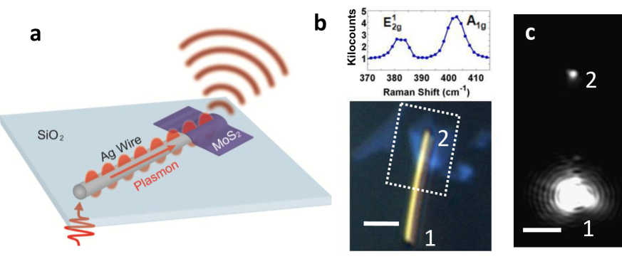
Figure 1a presents an illustration of the fabricated MoS2/Ag nanowire device. An incident photon is converted to a plasmon that propagates along the wire. When the plasmon arrives at the MoS2, the plasmon may either be converted to an exciton, resulting in frequency-shifted photon emission from the MoS2, or it can be converted back to a photon at the end of the wire. An optical micrograph of the hybrid device studied in this work is shown in the bottom panel of Fig. 1b. The top panel is a Raman spectrum acquired at the overlap region between the end of the nanowire and the MoS2. The measured Raman spectrum reveals that the flake is single-layer MoS242. See the Methods section for details on the fabrication of the device.
The charge-coupled device (CCD) image in Fig. 1c demonstrates plasmon propagation and photon re-emission. Laser radiation ( = 635 nm), polarized parallel to the wire axis, is coupled from the far-field into the nanowire at the end labeled “1” in Fig. 1b using a 100 oil-immersion objective with numerical aperture (NA) of 1.3. The power at the sample is 20 W. To reduce scattering and eliminate leakage radiation, the sample was covered in index-matching (n = 1.515) oil. In order to convert a photon into an SPP, the laser must be focused onto one of the ends of the wire; this accounts for the momentum mismatch between the incoming photon and the plasmon19. Due to confinement of the SPP modes, smaller-diameter wires yield shorter 1/ propagation lengths31, 43. In addition, the SPP 1/ propagation length increases as the optical excitation wavelength increases6. The wires used in our study support two lower-order modes. When the incident light is polarized parallel to the wire, the light couples to the lowest-order, SPP mode (Fig. 1c), and light oriented perpendicular to the wire couples to the mode22 (see Supplementary Fig. 1e and 1f). The in-coupling efficiency is always greater for the mode than for the mode, but the 1/ propagation length of the mode becomes longer for larger diameter wires, explaining why SPP propagation still occurs when incoming light is polarized perpendicular to the wire. For a wire of this length, we calculate the efficiency of photon re-emission at the end of the wire after plasmon propagation to be around 0.008% to 0.012%. See Supplementary Discussion 1 and Supplementary Fig. 1 for a discussion of photon re-emission efficiencies.
Optical interaction between the nanowire and MoS2
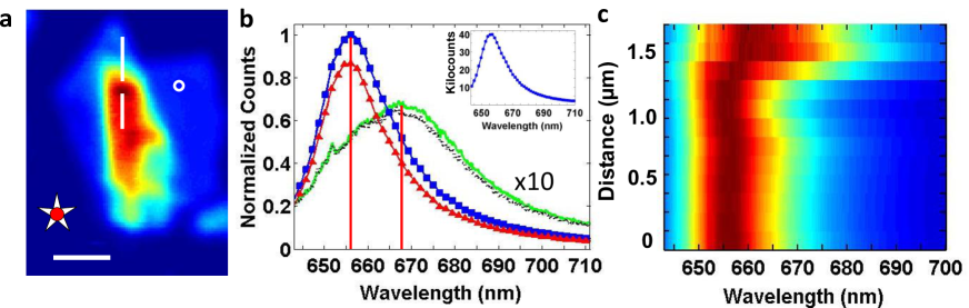
Coupling between far-field photons, SPPs, and the single-layer MoS2 was studied using an inverted confocal microscope utilizing an oil-immersion objective (NA = 1.4). See the Methods section for more details. A fluorescence image of the single-layer flake on the wire from Fig. 1b (region is outlined with dashed white box) is shown in Fig. 2a. For photon counting images, we adopt the convention of using a solid red circle to indicate the excitation and a white star to represent the approximate center of the collection focal volume, respectively. For this data set, the excitation and collection focal volumes are coincident so the dot and star overlap indicating no displacement between excitation and collection; however, later images introduce displacement of the excitation with respect to the collection. In Fig. 2a, we observe strong direct band gap PL from the MoS2 flake, characteristic of single-layer, as well as a large increase in counts in the area where the flake overlaps with the wire. To investigate the origin of the increased counts, Fig. 2b presents spectra acquired with the excitation polarization parallel and perpendicular to the wire on the bare flake (white circle in Fig. 2a) and at the wire-flake overlap region (break in the solid vertical line in Fig. 2a). Spectra taken at the wire-flake overlap region (bare flake) with excitation polarized parallel to the wire is shown in blue (green), and the red (black) curve shows the perpendicular polarization case. There can be a number of contributing effects to this enhancement. First, by removing direct contact with the substrate, MoS2 fluorescence is known to increase34, 44. Second, the enhancement of the MoS2 fluorescence when the excitation is polarized parallel to the nanowire is a manifestation of an antenna-like enhancement of the excitation field. In contrast, the PL intensity from the MoS2 on the substrate does not exhibit dependence on the excitation polarization. The enhancement in MoS2 fluorescence in the vicinity of the region where the Ag nanowire end overlaps with the MoS2 flake is consistent on all devices we have fabricated (see Supplementary Fig. 2 for data from four other single-layer devices, Supplementary Fig. 3 for a bilayer sample, and Supplementary Fig. 4 for a device that exhibits a 40-fold enhancement).
In addition to the enhancement, there is a clear spectral shift in the peak of the PL for the MoS2 over the wire (656 nm) compared to on the substrate (668 nm). We attribute this shift to the MoS2 flake not being in direct contact with the Ag nanowire as a result of the transfer process. The main PL peak of single-layer MoS2 consists of two peaks: the A peak centered at 655 nm attributed to uncharged excitons and the A- peak centered around 670 nm due to negatively-charged trions45. It has been reported that interaction of the MoS2 with the substrate suppresses exciton emission due to doping44. When removed from the substrate, the A peak becomes dominant. This shift is not due to strain, as strain would redshift the spectra46. For comparison, Fig. 2c presents MoS2 spectra as we measure along the line in Fig. 2a, starting from the bottom. Each spectrum is independently normalized. The spectral position of the peak is consistent along the wire covered by the MoS2, and as the collection region moves off of the wire, the peak redshifts. See Supplementary Fig. 5 for spatially-resolved Raman spectra of the same line cut and both Raman and PL along the line orthogonal to the vertical white line in Fig. 2a.
Plasmonic excitation of MoS2
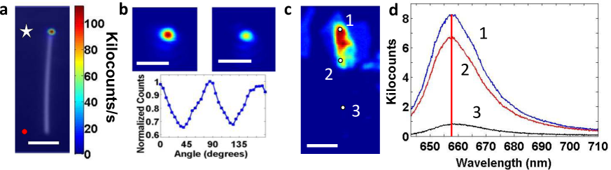
To explore plasmon excitation of MoS2 PL, the collection and excitation focal volumes are displaced vertically by the length of the wire. Figure 3a shows the resulting fluorescence image when the sample is scanned in this configuration with the laser polarized parallel to the wire. A CCD image of the MoS2/wire structure is overlayed on this image. The prominent feature in the fluorescence image results when the laser excites plasmons at the end of the wire opposite the MoS2, which propagate along the wire and excite MoS2 PL. Figure 3b displays scans of this feature when light is polarized parallel (upper left panel) and perpendicular (upper right panel) to the wire. There is a reduction in intensity when the light is polarized perpendicular to the wire, suggesting that this feature is the result of plasmon propagation. The bottom panel of Fig. 3b shows the normalized polarization dependence of the signal with a visibility of 21%. While the large-diameter Ag wire has modes that can be excited with an incident field polarized parallel or perpendicular to the wire, the observed modulation indicates that the coupling is stronger when the excitation is parallel. The largest visibility that we observed on a device was 80% (see Supplementary Fig. 6). Simulations using the finite-difference time-domain (FDTD) method in Lumerical to further investigate the plasmon excitation are shown in Supplementary Fig. 7.
We anticipate that plasmon-excited MoS2 PL is not limited to the end of the wire. To investigate this, the displacement between the laser excitation and collection was adjusted to be a fraction of the wire length. The sample is then translated so that the laser excitation is at the uncovered end of the wire. For reference, Fig. 3c shows a fluorescence scan of the full sample with circles to mark the effective positions of the spectral collection along the wire. Figure 3d presents the spectra corresponding to each of these points, starting from the top circle, labeled “1”, and walking downward in Fig. 3c. We observe that the PL is strongest near the end of the wire. However, we also obtain significant signal over the entire length that the wire is covered by the MoS2. This is suggestive of two mechanisms at play. First, plasmons that propagate to the end of the wire are rescattered as photons and reabsorbed by the MoS2, exciting an exciton. The electron-hole recombination then produces the PL signal. Second, plasmons in the wire are directly converted to excitons in the MoS2, which then fluoresces. The exact separation between the nanowire and the MoS2 flake determines the efficiency of direct plasmon absorption.
Plasmon extraction from MoS2 fluorescence
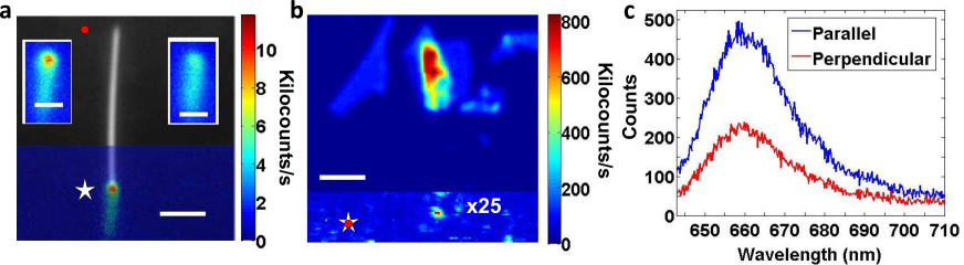
In addition to plasmons exciting the MoS2, the reverse process can also occur; that is, excitons in the MoS2 can be converted to plasmons that propagate along the wire and are rescattered as photons. To demonstrate that MoS2 fluorescence can couple to Ag nanowire plasmons, the excitation is aligned with the overlap region of the MoS2 flake/nanowire end, and the collection focal volume is aligned to the uncovered nanowire end (the reverse configuration of Fig. 3). Figure 4a shows the resulting fluorescence image when the sample is scanned in this configuration with the excitation laser polarized parallel to the wire. Again, a CCD image of the MoS2/wire structure is overlayed on this image. Compared to the localized feature in Fig. 3a, the present image shows an attribute that extends beyond the end of the wire. This is suggestive of plasmonic excitation along the MoS2/wire interface, not just at the covered end. As the laser excitation scans over the MoS2/wire interface, photons that re-emerge from the uncovered end are still detected by the confocal volume of the APD. If plasmons could only be excited at the end of the wire and not along the length of the MoS2/wire overlap, the attribute in this image would look similar to the feature in Fig. 3a. The insets display scans of the feature when the excitation light is polarized both parallel (upper left) and perpendicular (upper right) to the wire. Evident from comparing the two insets is an increase in the emission from the uncovered end when the excitation is parallel to the nanowire axis. The enhancement again suggests the nanowire provides an antenna-like enhancement of the excitation. Because MoS2 absorption does not prefer a linear polarization, any mismatch results from excitation effects.
Finally, we demonstrate it is possible to use the Ag nanowire both as a channel for near-field excitation of the MoS2 flake and to recollect the resultant MoS2 fluorescence. The re-excited plasmons, at the MoS2 photon energy, can propagate back along the wire and rescatter to the far-field as photons. Figure 4b shows a fluorescence image of the entire sample with the excitation and collection aligned. For this image, we have rescaled the end of the wire not covered by the MoS2. There is a pronounced fluorescence feature at the excitation end of the wire that is stronger than the background. To investigate this feature, spectra were collected for light polarized parallel and perpendicular to the wire (Fig. 4c). The spectra reveal this is indeed PL from the MoS2 flake; see Fig. 2b for comparison. The pronounced polarization contrast in the two different excitation directions suggests that the Ag nanowire plasmons mediate this excitation and collection process.
In summary, we have demonstrated photonic and plasmonic interactions between an individual Ag nanowire and single-layer MoS2. We found it is possible to excite MoS2 with Ag nanowire plasmons as well as convert decaying MoS2 excitons into Ag wire plasmons. This first step shows that there is pronounced nanoscale light-matter interaction between plasmons and atomically-thin material that can be exploited for nanophotonic integrated circuits. A natural next step is the creation of a near-field detector based on MoS2 as well as MoS2 light-emitting diodes coupled to on-chip nanoplasmonic circuitry.
Methods
Sample fabrication
A solution of silver nanowires (Nanostructured and Amorphous Materials, Inc.) with 386 nm average diameter and 8.6 m average length is diluted at a 2000:1 ratio of ethanol to solution, and a small amount (150 L) is stamped onto a clean silica coverslip using a polycarbonate membrane filter (5 m pore diameter, SPI Supplies, Inc.). The coverslip was placed in a petri dish with a hole bored in it and held in place with rubber cement for the transfer. On a separate silicon substrate with 270 nm of oxide (Si/SiO2), we exfoliated MoS2 from the bulk (SPI Supplies, Inc.) by micromechanical cleavage using adhesive tape (Semicorp). The optical interference due to the thickness of the oxide allows for identification of single-layers47, which is also confirmed by Raman spectroscopy (Fig. 1b top panel)42. The flakes were lifted off using a poly(methyl methacrylate) (PMMA)-based technique48, 49. After a candidate MoS2 flake is found on the Si/SiO2, two coats of 495K PMMA and one coat of 950K PMMA were spun onto the Si/SiO2; the sample was baked for 5 minutes at 105∘ C then immersed in 1 M NaOH at 80∘ C until release begins (about 10 minutes). It was transferred to deionized (DI) water, where the PMMA film was detached with assistance from tweezers. The petri dish with the wire sample was then filled with DI water, and a suitable wire was found using an inverted microscope with a long working distance objective. The PMMA film was transferred to the petri dish, and a post with a teflon-coated end attached to a micropositioner was brought into contact with the PMMA. Using a Harvard PhD 2000, the water was pumped from the petri dish; the objective focus could be adjusted to position the flake over the wire. The sample dried before immersion in an acetone bath to dissolve the PMMA.
Optical characterization
The samples were characterized with an inverted microscope equipped with an oil-immersion objective. A nanopositioning stage (Mad City Labs, Inc.) was used to scan and position the sample. The sample was characterized using a 532 nm wavelength laser for Raman spectroscopy or a 633 nm wavelength laser for photoluminescence and plasmon propagation measurements. Excitation polarization was controlled by a half-wave plate. The signal from the sample was sent to either an APD or a spectrometer. Longpass filters to block the laser line were used in front of both detectors. For some of the fluorescence images, a similar second set-up with a 635 nm wavelength laser was used. Laser power of 5 W was used in Fig. 2, Fig. 3, and Fig. 4b and 4c. Laser power of 20 W was used in Fig. 1c and Fig. 3a. Laser power of 70 W was used in Fig. 1b.
References
- 1 Rattner, J. Plenary: The future of silicon photonics. In Integrated Photonics Research, Silicon and Nanophotonics and Photonics in Switching, JTuA1 (Optical Society of America, 2010).
- 2 Sorger, V. J., Oulton, R. F., Ma, R.-M. & Zhang, X. Toward integrated plasmonic circuits. MRS Bulletin 37, 728–738 (2012).
- 3 Huang, K. C. Y. et al. Electrically driven subwavelength optical nanocircuits. Nat. Photon. 8, 244–249 (2014).
- 4 Novotny, L. & Hecht, B. Principles of Nano-Optics (Cambridge University Press, Cambridge, 2006).
- 5 Maier, S. A. Plasmonics: Fundamentals and Applications (Springer, New York, 2007).
- 6 Barnes, W. L., Dereux, A. & Ebbeseni, T. W. Surface plasmon subwavelength optics. Nature 424, 824–830 (2003).
- 7 Ozbay, E. Plasmonics: Merging photonics and electronics at nanoscale dimensions. Science 311, 189–193 (2006).
- 8 Maier, S. A. & Atwater, H. A. Plasmonics: localization and guiding of electromagnetic energy in metal/dielectric structures. J. Appl. Phys. 98, 011101 (2005).
- 9 Bozhevolnyi, S. I., Volkov, V. S., Devaux, E., Laluet, J.-Y. & Ebbesen, T. W. Channel plasmon subwavelength waveguide components including interferometers and ring resonators. Nature 440, 508–511 (2006).
- 10 Oulton, R. F., Sorger, V. J., Genov, D. A., Pile, D. F. P. & Zhang, X. A hybrid plasmonic waveguide for subwavelength confinement and long-range propagation. Nat. Photon. 2, 496–500 (2008).
- 11 Pacifici, D., Lezec, H. J. & Atwater, H. A. All-optical modulation by plasmonic excitation of cdse quantum dots. Nat. Photon. 1, 402–406 (2007).
- 12 Beams, R. et al. Nanoscale fluorescence lifetime imaging of an optical antenna with a single diamond NV center. Nano Lett. 13, 3807–3811 (2013).
- 13 Ditlbacher, H. et al. Silver nanowires as surface plasmon resonators. Phys. Rev. Lett. 95, 257403 (2005).
- 14 Laroche, T. & Girard, C. Near-field optical properties of single plasmonic nanowires. Appl. Phys. Lett. 89, 233119 (2006).
- 15 Zou, C.-L. et al. Plasmon modes of silver nanowire on a silica substrate. Appl. Phys. Lett. 97, 183102 (2010).
- 16 Wei, H., Zhang, S., Tian, X. & Xu, H. Highly tunable propagating surface plasmons on supported silver nanowires. Proc. Natl. Acad. Sci. U.S.A 110, 4494–4499 (2013).
- 17 Chang, D. E., Sørensen, A. S., Hemmer, P. R. & Lukin, M. D. Quantum optics with surface plasmons. Phys. Rev. Lett. 97, 053002 (2006).
- 18 Manjavacas, A. & Garcia de Abajo, F. J. Robust plasmon waveguides in strongly interacting nanowire arrays. Nano Lett. 9, 1285–1289 (2009).
- 19 Sanders, A. W. et al. Observation of plasmon propagation, redirection, and fan-out in silver nanowires. Nano Lett. 6, 1822–1826 (2006).
- 20 Wang, W., Yang, Q., Fan, F., Xu, H. & Wang, Z. L. Light propagation in curved silver nanowire plasmonic waveguides. Nano Lett. 11, 1603–1608 (2011).
- 21 Li, Z. et al. Directional light emission from propagating surface plasmons of silver nanowires. Nano Lett. 9, 4383–4386 (2009).
- 22 Li, Z. et al. Correlation between incident and emission polarization in nanowire surface plasmon waveguides. Nano Lett. 10, 1831–1835 (2010).
- 23 Fang, Y. et al. Branched silver nanowires as controllable plasmon routers. Nano Lett. 10, 1950–1954 (2010).
- 24 Fedutik, Y., Temnov, V. V., Schöps, O., Woggon, U. & Artemyev, M. V. Exciton-plasmon-photon conversion in plasmonic nanostructures. Phys. Rev. Lett. 99, 136802 (2007).
- 25 Wei, H., Ratchford, D., Li, X., Xu, H. & Shih, C.-K. Propagating surface plasmon induced photon emission from quantum dots. Nano Lett. 9, 4168–4171 (2009).
- 26 Gruber, C., Trügler, A., Hohenau, A., Hohenester, U. & Krenn, J. R. Spectral modifications and polarization dependent coupling in tailored assemblies of quantum dots and plasmonic nanowires. Nano Lett. 13, 4257–4262 (2013).
- 27 Akimov, A. V. et al. Generation of single optical plasmons in metallic nanowires coupled to quantum dots. Nature 450, 402–406 (2007).
- 28 Shegai, T., Huang, Y., Xu, H. & Käll, M. Coloring fluorescence emission with silver nanowires. Appl. Phys. Lett. 96, 103114 (2010).
- 29 Huck, A., Kumar, S., Shakoor, A. & Andersen, U. L. Controlled coupling of a single nitrogen-vacancy center to a silver nanowire. Phys. Rev. Lett. 106, 096801 (2011).
- 30 Kolesov, R. et al. Wave-particle duality of single surface plasmon polaritons. Nat. Phys. 5, 470–474 (2009).
- 31 Falk, A. L. et al. Near-field electrical detection of optical plasmons and single-plasmon sources. Nat. Phys 5, 475–479 (2009).
- 32 Kim, J. et al. Electrical control of optical plasmon resonance with graphene. Nano Lett. 12, 5598–5602 (2012).
- 33 Qian, H. et al. Electrical tuning of surface plasmon polariton propagation in graphene-nanowire hybrid structure. ACS Nano 8, 2584–2589 (2014).
- 34 Mak, K. F., Lee, C., Hone, J., Shan, J. & Heinz, T. F. Atomically thin MoS2: A new direct-gap semiconductor. Phys. Rev. Lett. 105, 136805 (2010).
- 35 Splendiani, A. et al. Emerging photoluminescence in monolayer MoS2. Nano Lett. 10, 1271–1275 (2010).
- 36 Zeng, H., Dai, J., Yao, W., Xiao, D. & Cui, X. Valley polarization in MoS2 monolayers by optical pumping. Nat. Nanotech. 7, 490–493 (2012).
- 37 Mak, K. F., He, K., Shan, J. & Heinz, T. F. Control of valley polarization in monolayer MoS2 by optical helicity. Nat. Nanotech. 7, 494–498 (2012).
- 38 Cao, T. et al. Valley-selective circular dichroism of monolayer molybdenum disulphide. Nat. Commun. 3, 887 (2012).
- 39 Radisavljevic, B., Radenovic, A., Brivio, J., Giacometti, V. & Kis, A. Single-layer MoS2 transistors. Nat. Nanotech. 6, 147–150 (2011).
- 40 Yin, Z. et al. Single-layer MoS2 phototransistors. ACS Nano 6, 74–80 (2012).
- 41 Lopez-Sanchez, O., Lembke, D., Kayci, M., Radenovic, A. & Kis, A. Ultrasensitive photodetectors based on monolayer MoS2. Nat. Nanotech. 8, 497–501 (2013).
- 42 Lee, C. et al. Anomalous lattice vibrations of single- and few-layer MoS2. ACS Nano 4, 2695–2700 (2010).
- 43 Takahara, J., Yamagishi, S., Taki, H., Morimoto, A. & Kobayashi, T. Guiding of a one-dimensional optical beam with nanometer diameter. Opt. Lett. 22, 475–477 (1997).
- 44 Scheuschner, N. et al. Photoluminescence of freestanding single- and few-layer MoS2. Phys. Rev. B 89, 125406 (2014).
- 45 Mak, K. et al. Tightly bound trions in monolayer MoS2. Nat. Mater. 12, 207–211 (2013).
- 46 Conley, H. J. et al. Bandgap engineering of strained monolayer and bilayer MoS2. Nano Lett. 13, 3626–3630 (2013).
- 47 Benameur, M. M. et al. Visibility of dichalcogenide nanolayers. Nanotechnology 22, 125706 (2011).
- 48 Reina, A. et al. Transferring and identification of single- and few-layer graphene on arbitrary substrates. J. Phys. Chem. C 112, 17741–17744 (2008).
- 49 Sundaram, R. S. et al. Electroluminescence in single layer MoS2. Nano Lett. 13, 1416–1421 (2013).
Acknowledgements
The authors acknowledge support from the Institute of Optics, the U. S. Department of Energy (grant DE-FG02-05ER46207), the National Science Foundation IGERT program, and the National Science Foundation (DMR-1309734).
Author Contributions
R. B., L. N., and A. N. V. conceived the research. K. G. and C. C. fabricated the samples. K. G. and R. B. conducted the measurements. C. C. conducted the simulations. All authors discussed the data and wrote the manuscript.
Competing Financial Interests
The authors declare no competing financial interests.
See pages - of Supplement0404.pdf