Corresponding author. ]Tel.: +7 831 4623304;
E-mail address: maksimova.galina@mail.ru (G.M. Maksimova)
Transport in graphene nanostructures with spatially modulated gap and potential
Abstract
We study transport properties of graphene nanostructures consisted of alternating slabs of gapless and gapped graphene in the presence of piecewise constant external potential equal to zero in the gapless regions. The transmission through single-, double-barrier structures and superlattices has been studied. It was revealed that any -barrier structure is perfectly transparent at certain conditions defining the positions of new Dirac points created in the superlattice. The conductance and the shot noise were as well computed and investigated for the considered graphene systems. In a general case, existence of gapped graphene fraction leads to decrease of the conductance and increase of the Fano factor. For two barriers formed by gapped graphene and separated by a long and highly doped region the Fano factor rises up to 0.5 in contrast to the similar gapless structure where the Fano factor is close to 0.25. Similarly to a gapless graphene superlattice, creation of each new Dirac point manifests itself as a conductivity resonance and a narrow dip in the Fano factor. However, gapped graphene inclusion into the potential-barrier regions in the superlattice leads to more complicated dependence of the Fano factor on the potential height compared to pseudo-diffusive behaviour (with ) typical for a gapless superlattice.
I Introduction
Transport properties of graphene and graphene-based microstructures are currently among the most actively investigated topics in graphene physics Sarma ; Castro ; Peres ; Mucc ; Kats ; Tworz ; DiCarlo ; Dann ; Balandin ; Ghosh ; Novoselov . Aside from fundamental aspects such interest in graphene stems from its potential applications as a high-mobility semiconductor and the experimental ability to tune its properties via gating Castro . Investigation of the electron transport includes the consideration of a conductance and shot noise which is characterized by the Fano factor being the ratio of the noise power and mean current. For instance, the Fano factor of wide and short graphene sheet equals 1/3 Tworz near the Dirac point. This coincides with the well-known result for diffusive wire Beenakker .
Lots of theoretical and experimental works have been devoted to investigations of transmission and conductance through different multibarrier graphene nanostructures and graphene superlattices (SLs) Wang ; Huard ; Bliokh ; Krst ; Pell ; Gatt ; Pereira ; Brey ; Park ; Meyer ; Mar which can be fabricated, e.g., by applying a local top gate voltage. It has been shown that a one-dimensional periodic potential substantially affects the transport properties of graphene. For instance, the Kronig-Penny type electrostatic potential produces strong anisotropy in the carrier group velocity near the Dirac point leading to the supercollimation phenomenon Park1 ; Park2 ; Barbier .
The band structure of an ideal graphene sheet has no energy gap which results, for example, in total transparency of any potential barrier for normally-incident electrons Kats1 (an analog of the Klein paradox Klein ). It is extremely desirable for electronics applications that graphene structures be gapped. Therefore, much effort of researchers has been focused on producing a gap in the graphene spectrum. The gap can be created by strain engineering as well as by deposition or adsorption of molecules on a graphene layer. For instance, a hydrogenated sheet of graphene (graphane) is a semiconductor with a gap of the order of a few eV Leb . Other way of producing the gap is to use hexagonal boron nitride (hBN) substrate. In this case the gap value is small enough owing to the lattice mismatch. However, it can be increased by the applying of a perpendicular electric field Kind .
Creation of various graphene heterostructures, including SLs, with the gap discontinuity is widely discussed now. One way of generating spatially modulated gap is graphene on a substrate made from different dielectrics Ratn . The required gap modulation can also be created by using, e.g., an inhomogeneously hydrogenated graphene or graphene sheet with nonuniformly deposited CrO3 molecules. In our previous work Maks we studied the electronic properties of graphene SL in which the gap and potential profile are piecewise constant functions. It was found that in such SL up to some critical value of potential allowed subbands are separated by gaps. When the potential value is greater or equal to the contact or cone-like Dirac points appear in the spectrum. As a result, SL becomes gapless.
In this work we examine in detail ballistic transport through graphene nanostructures, including SL, formed by space-modulated gap and potential. Using the transfer-matrix formalism we study the transmission, conductance and the Fano factor for systems with arbitrary numbers of barriers.
II Basic equations
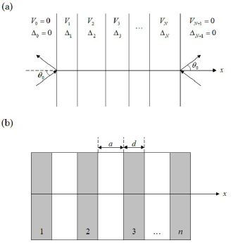
Let us initially consider a lateral one-dimensional multibarrier structure consisting of strips with widths characterized by the gaps and potential heights (see Fig. 1). The outer regions labeled by 0 and correspond to the gapless graphene with . In strip, the carriers are described by the two-dimensional Dirac equation
| (1) |
where is the momentum operator, is the vector of Pauli matrices, and is the Fermi velocity. Due to translation invariance in the -direction, the solution of Eq. (1) in region can be written as . It is convenient to define the wavevector as
| (2) |
Then for the wavefunction in strip is a superposition of plane waves
| (3) |
Here, , , , , . and denote the left and right boundaries of the strip , so that . In the opposite case, when , solution has pure exponential behaviour along the -axis.
Suppose that oscillates everywhere. Then we define the functions , . As a result, Eq. (II) may be written in the form
| (4) |
where
| (5) |
Continuity of the upper and lower components at the strip boundaries requires that
| (6) |
Within the region the solutions , and , are connected by the free propagation matrix :
| (7) |
where
| (8) |
Combining Eqs (7) and (8) one can find:
| (9) |
where the transfer matrix is introduced for the considered heterostructure as
| (10) |
Here is determined by Eq. (5) at and , which yields:
We may use Eq. (II) for an arbitrary multibarrier structure, characterized by different parameters and in each slab of width .
We now consider scattering of a Dirac particle on the graphene superstructure consisted of gapped graphene strips of width and gapless graphene strips of width . Then and equal and , respectively, in the gapped regions and zero elsewhere. In this case the transfer matrix can be written in the form
| (12) |
where expressions for the matrices and are given in the Appendix [Eqs (A) and (A)]. If is large enough, it is convenient to use the -representation in which matrix is diagonal. The diagonalization procedure is a transform with
| (13) |
where
| (14) |
Then,
| (15) |
where
| (16) |
Using the above relations we obtain the final expression for the transfer matrix
| (17) |
Supposing that the incoming wave is scattered on the left border of the structure, we set , , and . Here and are the amplitudes of the reflected and transmitted states. Then the transmission probability is given by
| (18) |
Substituting Eqs (5), (13)–(15), and (A) into Eq. (17 ), one obtains
| (19) |
where matrix elements are defined by Eq. (A).
III Tunneling through multiple barriers
We first consider the single-barrier geometry when the gapped graphene strip of width borders on the gapless graphene. Using Eq. (A) one has
Here the wave vector is defined in the barrier region and also depends on the angle of incidence (or ):
| (21) |
Eq. (III) is a generalization of two cases: , Kats2 and , Gomes . The transmission described by Eq. (21) oscillates as a function of barrier width with a period depending on the wavevector . Such behaviour takes place at all initial angles when the particle energy , where
| (22) |
Note that, at the wave vector is the same for both gapped and gapless regions. If the energy satisfies the conditions or similar oscillating dependence holds only for the angles of incidence , where
| (23) |
When exceeds the critical angle , is pure imaginary and the transmission is determined by the evanescent states in barrier region
| (24) |
where
| (25) |
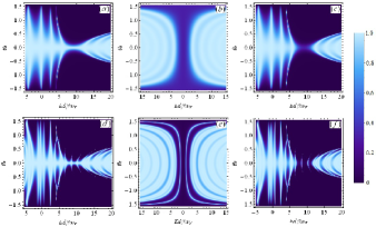
These expressions also describe the transmission through the barrier at all angles for the energies lying inside the gap: . To illustrate the dependence of the transmission on both the energy and the angle of incidence we construct a density plot of . The different colors from black to white correspond to different values of from 0 to 1. Such a density plot for a single barrier of width nm is shown in figures 2(a)–2(c) at various ratios between and . For a gapless graphene it is clearly seen (Fig. 2(a)) the perfect transmission for normal or near-normal incidence , which is a manifestation of Klein tunneling. The opening gap in the barrier region suppresses this effect (figures 2(b), 2(c)). The barrier becomes also completely transparent for values , where is integer. As follows from Eq. (21) these resonances are well-defined at close to . Corresponding resonant energies weakly depend on the gap value for (figures 2(a), 2(c)). On the contrary, when applied potential and is not too large , the transmission probability is about 1 in the wide region of ; plane (Fig. 2(b)).
To calculate the transmission through a double-barrier structure we use the expression for the real and imaginary parts of (A), (A). The results are illustrated in figures 2(d)–2(f) for a symmetrical case when the barrier width coincides with the interbarrier separation . Pronounced resonant structure is seen in the energy interval caused by the quasibound states in the well region.
Note, that for identical barriers the matrix element (III) depends on through the factors , where the eigenvalues and of the matrix define the band structure of infinite periodic SL with period Maks according to equation , where is the Bloch wavevector. Thus, the infinite periodic structure is transparent when . As follows from Eq. (II), arbitrary -barrier structure becomes perfectly transparent for some angles of incidence in special case when and . Here the resonant angles are given by

| (26) |
We should emphasize also that, the above conditions (22) and (26) for existence of resonances in the transmission probability of -barrier structure correspond to the positions of new cone-like Dirac points in -space in the infinite SL Maks .
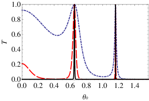
Angular dependence of the transmission coefficients is shown in Fig. 3 for and meV, meV. As seen, the positions and number of resonant peaks are defined by and do not change with increasing the number of barriers . On the contrary, the widths of resonances decrease as increases. As a result, graphene superlattice becomes opaque for almost all angles of incidence except for (see Fig. 3 for ). Such a dependence with is similar to the dependence of the transmission of electromagnetic waves in the periodic structure made of dielectric layers with refractive indices Bliokh ; Wu . The signs correspond, respectively, to dielectrics with positive (right-handed ()) and negative (left-handed ()) refractive indices.
The analogies between the charge transport in graphene structures and propagation of light in layered dielectric media have been discussed earlier Bliokh ; Che ; Bliokh1 . It was shown that the difference in a gapless graphene plays the same role as the refractive index in dielectric structure. In particular, focusing the electric current by a single junction in graphene was predicted, which is similar to focusing the electromagnetic waves by the - interface Che . In our case (Fig. 3) the states with belong to the conduction band in gapless region and to the valence band in gapped region, so that the considered superlattice is similar to the symmetric - periodic dielectric structure. Note also that the existence of gapped fraction in graphene leads to suppression of Klein tunneling. This means that analogous - periodic structure is characterized by different impedances. When is negative, the angular dependence of drastically changes (Fig. 4). As seen, there are many angles other than , for which the transmission is also one. In this case the graphene multibarrier structure has transport properties resembling to the transmission of light through a stack of dielectric layers with the same refractive indices and different impedances Bliokh .
IV Conductance and shot noise
Basing on the obtained results for the transmission probabilities , one can find the two-terminal Landauer conductance and the Fano factor for the finite periodic-potential-gap structure. Within a linear regime on bias voltage at very low temperatures they are given by
| (27) |
| (28) |
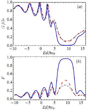
with and the length of the slab in the -direction. equals 4 due to the twofold spin and valley degeneracy. In Fig. 5 we plot the conductance (a) and the Fano factor (b) versus the Fermi energy for a single potential-gap barrier of width nm for meV and meV (solid line), meV (dashed line), and (dash-dotted line). In the considered case for we model the leads (the gapless region) by highly doped graphene.
At the conductance minimum and the Fano factor at the Dirac point (at ) coincide with the ones obtained by Tworzydlo et al. Tworz
| (29) |
With the gap increasing, the minimum value of the conductance decreases while the maximum value of the Fano factor approaches 1. Inside the gap i.e. for (for meV) and (for meV) the dependencies and become almost flat (Fig. 5). When and one can find the approximate expressions for and :
| (30) |
| (31) |
where is the modified Bessel function of argument and .
The results discussed above were obtained at small bias voltage between the leads and the sheet. In this case the main contribution to the current and shot noise comes from the evanescent states. At high voltages we have take into account the propagating waves also. This leads to increase of the conductance and decrease of the Fano factor. Specifically, for a gapless graphene sheet the Fano factor drops from 1/3 at low voltages to 0.125 at high voltages Sonin . Thus, we may suppose, that for , the conductance and the Fano factor are nearly independent of finite value of voltage drops up to .
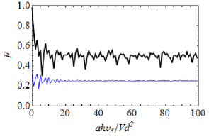
We have studied the double-barrier structure formed by two gapped graphene regions of width separated by highly doped region of width . In Fig. 6 we plot the Fano factor (at ) as function of interbarrier spacing at meV, nm, (thin line) and meV (thick line). It is clearly seen that for two gapless graphene strips kept at the Dirac point and separated by an extensive and highly doped region the Fano factor oscillates near the value 0.25 in accordance with analytic calculations presented in ref. Wiener1 . For and , the similar calculations yield . For small values of the Fano factor in these cases approaches 1/3 and 1 correspondingly.
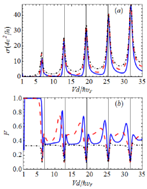
Now let us consider -periodic (i.e. region in Fig. 1(b), with ) symmetric structure. We choose periodic structure modeling general physical properties of a superlattice. As was already shown Maks , depending on the potential barrier height , the band structure of such SL can have more than one Dirac point located at (23). In contrast to the SLs discussed, e.g., in Brey ; Barbier , the Dirac point being a prototype of the original Dirac point (situated at ) arises at certain values of :
| (32) |
which are the solutions of equation , where
In this case the total number of Dirac points is . When the ratio is not integer, the number of the Dirac points symmetrically located around is given by , where denotes an integer part.
Fig. 7 shows the conductivity and the Fano factor at (23) as a function of for three symmetric ( nm) multibarrier structures characterized by different gap values in the barrier regions: meV (solid line), meV (dashed line), and (dash-dotted line). Vertical lines indicate the positions of which weakly depend on for (32). As seen, each a new Dirac point manifests itself as a conductivity resonance and a narrow dip in the Fano factor. Between the resonances at the system demonstrates pseudo-diffusive behaviour similarly to Fertig . The existence of gapped graphene fraction in barrier regions leads to decrease of the conductivity and strongly affects the Fano factor. Independently of the gap value , the Fano factor of the gapped SL equals 1 almost in the whole region that differs from for gapless graphene SL (Fig. 7(b)). Such difference is caused by the qualitative distinction in the electronic spectrum of two types of the SLs in this range of . For gapless SL prototype of the original Dirac point always exists in the energy spectrum. On the contrary, at there is a minigap separating the conduction and valence minibands in the SL with . This results in a nearly zero transmission at , and, correspondingly, . At more complicated Fano factor dependence takes place in the nonresonant domains due to nonmonotonic dependence of the transmission probability in contrast to the case when the perfect transmission occurs at . At large heights of the potential, minimum value of increases and becomes smoother function of between the dips.
V Conclusion
In summary, based on the transfer-matrix method, we have investigated the conductance and Fano factor as well as the angular and energy dependencies of the transmission probability for one-dimensional graphene multibarrier structures. In our study we do not consider distinction in the Fermi velocities in gapped and gapless graphene fractions that can arise, e. g., in graphene deposited on the various substrates, or in appropriately doped graphene Tap .
In general case increasing the number of barriers in the considered heterostructures causes an appearance of extra peaks in transmission probability. It was found that symmetric -barrier structure is perfectly transparent for some angles of incidence (26) at the particle energy (22). If both electronic (in the well regions) and hole (inside the barrier) states contribute to the formation of the propagating modes. In this case the positions and number of resonant peaks do not depend on the barrier number . However increase of leads to the decrease of their widths, so that for the propagation of particles through 1D-graphene structure is similar to the propagation of electromagnetic waves through symmetric dielectric system composed of right- and left-handed materials.
Also, we have investigated the effect of gapped graphene fraction on the conductivity and shot noise. As expected, the inclusion of gapped graphene results in a decrease of the conductance and increase of the Fano factor. At the same time, existence of gapped-graphene regions in the structure affects the Fano factor considerably stronger than the conductivity. We have computed the conductivity and the Fano factor of the SL at (22) depending on . It was shown that each a new Dirac point in the SL with modulated gap manifests itself as a conductivity resonance and a narrow dip in the Fano factor similarly to a gapless SL. Between resonances the behaviour of is more complicated and different from pseudo-diffusive behaviour typical for SL with . It was also shown, that irrespective of the gap value in the range of potential values the Fano factor equal 1 for gapped SL unlike value 1/3 for a gapless SL.
Appendix A
Since the multibarrier structure consists of two kinds of graphene strips, there are two different matrices and
| (33) |
| (34) |
with , , , , , .
As was noted above, we suppose that where . Let the superlattice contain barrier regions of width . Then it is easy to see from Eq. (10), that , where and . Using Eqs. (5), (33) and (34) after some algebra we obtain
| (35) |
| (36) |
and
The above expressions allow us to find the matrix element determining the transmission (II). Thus for a single barrier one obtains
| (38) |
The value corresponds to the transmission of electron through a symmetrical double barrier structure. In this case
| (39) |
| (40) |
Acknowledgments
We are grateful to Dr. Burdov for his interest in this investigation and for helpful remarks. This work was supported by the Russian Foundation for Basic Research (Grant No 13-02-00784)
References
- (1) S. Das Sarma, S. Adam, E.H. Hwang, and E. Rossi, Reviews of Modern Physics 83, 407 (2011).
- (2) A.H. Castro Neto, F. Guinea, N.M.R. Peres, K.S. Novoselov, and A.K. Geim, Reviews of Modern Physics 81, 109 (2009).
- (3) N.M.R. Peres, Journal of Physics: Condensed Matter 21, 323201 (2009).
- (4) E.R. Mucciolo and C.H. Lewenkopf, Journal of Physics: Condensed Matter 22, 273201 (2010).
- (5) M.I. Katsnelson, European Physical Journal B 51, 157 (2006).
- (6) J. Tworzydlo, B. Trauzettel, M. Titov, A. Rycerz, and C.W.J. Beenakker, Physical Review Letters 96, 246802 (2006).
- (7) L. DiCarlo, J.R. Williams, Y. Zhang, D.T. McClure, and C.M. Marcus, Physical Review Letters 100, 156801 (2008).
- (8) R. Danneau, F. Wu, M.F. Craciun, S. Russo, M.Y. Tomi, J. Salmilehto, A.F. Morpurgo, and P.J. Hakonen, Physical Review Letters 100, 196802 (2008).
- (9) A.A. Balandin, S. Ghosh, W. Bao, I. Calizo, D.Teweldebrhan, F. Miao, and C.N. Lau, Nano Letters 8, 902 (2008).
- (10) S. Ghosh, I. Calizo, D. Teweldebrhan, E.P. Pokatilov, D.L. Nika, A.A. Balandin, W. Bao, F. Miao, and C.N. Lau, Applied Physics Letters 92, 151911 (2008).
- (11) K.S. Novoselov, A.K. Geim, S.V. Morozov, D. Jiang, Y. Zhang,S.V. Dubonos, I.V. Grigorieva, A.A. Firsov, Science 306, 666 (2004).
- (12) C.W.J. Beenakker, Reviews of Modern Physics 69, 731 (1997).
- (13) L.-G. Wang and S.-Y. Zhu, Physical Review B 81, 205444 (2010).
- (14) B. Huard, J.A. Sulpizio, N. Stander, K. Todd, B. Yang, and D. Goldhaber-Gordon, Physical Review Letters 98, 236803 (2007).
- (15) Y.P. Bliokh, V. Freilikher, S. Savel’ev, and F. Nori, Physical Review B 79, 075123 (2009).
- (16) P.M. Krstajić and P. Vasilopoulos, Journal of Physics: Condensed Matter 23, 135302 (2011).
- (17) F.M.D. Pellegrino, G.G.N. Angilella, and R. Pucci, Physical Review B 84, 195404 (2011).
- (18) S. Gattenlöhner, W. Belzig, M. Titov, Physical Review B 82, 155417 (2010).
- (19) J.M. Pereira Jr., P. Vasilopoulos, and F.M. Peeters, Applied Physics Letters 90, 132122 (2007).
- (20) L. Brey and H.A. Fertig, Physical Review Letters 103, 046809 (2009).
- (21) C.H. Park, Y.W. Son, L. Yang, M.L. Cohen, and S.G. Louile, Physical Review Letters 103, 046808 (2009).
- (22) J.C. Meyer, C.O. Giret, M.F. Crommie, and A. Zettl, Applied Physics Letters 92, 123110 (2008).
- (23) S. Marchini, S. Günther, and J. Wintterlin, Physical Review B 76, 075429 (2007).
- (24) C.-H. Park, Y.-W. Son, L. Yang, M.L. Cohen, and S.G. Louile, Nature Physics 4, 213 (2008).
- (25) C.-H. Park, Y.-W. Son, L. Yang, M.L. Cohen, and S.G. Louile, Nano Letters 8, 2920 (2008).
- (26) M. Barbier, P. Vasilopoulos, and F.M. Peeters, Physical Review B 81, 075438 (2010).
- (27) M.I. Katsnelson, K.S. Novoselov, and A.K. Geim, Nature Physics 53, 620 (2006).
- (28) O. Klein, Zeitschrift für Physics 53, 157 (1929).
- (29) S. Lebeque, M. Klintenberg, O. Eriksson, and M.I. Katsnelson, Physical Review B 79, 245117 (2009).
- (30) M. Kindermann, B. Uchoa, D.L. Miller, Physical Review B 86, 115415 (2012).
- (31) P.V. Ratnikov, JETP Letters 90, 469 (2009).
- (32) G.M. Maksimova, E.S. Azarova, A.V. Telezhnikov, and V.A. Burdov, Physical Review B 86, 295422 (2012).
- (33) M.I. Katsnelson, K.S. Novoselov, and A.K. Geim, Nature Physics 2, 620 (2006).
- (34) J.V. Gomes and N.M.R. Peres, Journal of Physics: Condensed Matter 20, 325221 (2008).
- (35) L. Wu, S. He, and L. Shen, Physical Review B 67, 235103 (2003).
- (36) V. Cheanov, V. Fal’ko, and B. Altshuler, Science 315, 1252 (2007).
- (37) Y.P. Bliokh, V. Freilikher and F. Nori, Physical Review B 87, 245134 (2013).
- (38) E.B. Sonin, Physical Review B 77, 233408 (2008).
- (39) A.D. Wiener and M. Kindermann, Physical Review B 84, 245420 (2011).
- (40) H.A. Fertig and L. Brey, Philosophical Transactions of the Royal Society A 368, 5483 (2010).
- (41) L. Tapasztó, G. Dobric, P. Nemes-Incze, G. Vertesy, Ph. Lambin and L.P. Biró, Physical Review B 78, 233407 (2008).