Half metallic and insulating phases in BN/Graphene lateral heterostructures
Abstract
We investigate theoretically the electronic structure of graphene and boron nitride (BN) lateral heterostructures, which were fabricated in recent experiments. The first-principles density functional calculation demonstrates that a huge intrinsic transverse electric field can be induced in the graphene nanoribbon region, and depends sensitively on the edge configuration of the lateral heterostructure. The polarized electric field originates from the charge mismatch at the BN-graphene interfaces. This huge electric field can open a significant bang gap in graphene nanoribbon, and lead to fully spin-polarized edge states and induce half-metallic phase in the lateral BN/Graphene/BN heterostructure with proper edge configurations.
pacs:
73.40.-c, 73.22.Pr, 75.76.+jTwo-dimensional (2D) materials are promising to achieve the essential requirements for future flexibleflexible1 ; flexible2 , high speed and low power-consumption electronic devices. Electrons in these 2D atomic crystals such as graphene, hexagonal boron nitride (hBN), molybdenum disulphide (MoS2), other dichalcogenides and layered oxidesgraphene1 ; graphene2 ; MoS21 ; MoS22 ; BN ; 2D ), behave like massless and massive Dirac fermionsgrapheneES , and display unique transportgrapheneTr1 ; grapheneTr2 and optical propertiesgrapheneOp , such as Klein tunnelingklein , half-integer quantum Hall effect at room temperatureHall1 ; Hall2 and valley-spin lockingvalleyspin . Recently, different isolated atomic crystals can be assembled into designing heterostructures layer by layer via van del Waals force between these 2D materials. These remarkable man-made new materials reveal unusual properties and novel phenomenavdW1 ; vdW2 ; vdW3 ; vdW4 ; vdW5 . Very recently, in-plane lateral heterostructures between graphene and hexagonal boron nitride have been fabricated with controlled domain sizes and shaped as combs, bars and ringslateral1 ; lateral2 . The lateral heterostructure between graphene and hBN is particular important since graphene is gapless semimetal whereas a monolayer of hBN is an insulator with a wide bandgap of 5.9eV, and different atomic compositions may coexist within continuous atomically thin films and many well-developed techniques have been realized or attempted in graphene. The hybridized in-plane heterostructures could provide us tremendous oppotunities towards atomically thin integrated circuitry. With proper control the interface between graphene/hBN, the bandgap and spin-relevant property could be precisely engineered, which are essential parts in electronics.
Electronic transport in graphene is the subject of intense interest at present. It might also be a promising material for spintronics and quantum information and computation, owing to the low intrinsic spin-orbit interaction, as well as the low hyperfine interaction of the electron spins with the carbon nuclei.spingra1 ; spingra2 ; spingra3 ; spingra4 ; spingra5 ; spingra6 ; QCgra ; maggra1 ; maggra2 ; Allen Recent theoretical and experimental results show that graphene could be the long-awaited platform for spintronics, since graphene possesses the extremely long spin diffusion length (100) and high mobility at room temperature. This could be a unique advantage for spintronic devices, particularly for logic circuits in which information is coded by spin or pseudo-spin (valley). It is interesting that despite there is no d band electrons, edge states in zigzag graphene nanoribbons (GNR) are spin polarized with large magnetic interaction and ferromagnetically ordered at each side. The spins at the two sides are oriented antiparallelly. This spin distribution at the edges of GNR inspired an interesting idea that a strong transverse electric field may drive the system into half metallic phase,Louie which is an intriguing class of materials, possessing metallic phase for electrons with one spin orientation, but insulating for electrons with the other. Fully spin-polarized electrical current in such systems holds significant promise for spintronic devices. The spin property of half-metal stimulates substantial efforts to search for half-metallic materials containing d-shell electrons, for example, Heusler alloys and manganese perovskite. However, in zigzag GNRs, one can relaize the half-metallic phase under an in-plane electric field which is required very high. For a GNR with 32 zigzag chains (32-GNR), one needs to apply 4.5 MV/cm-1 electric field to achieve the half metallicity. The field needed becomes larger for a narrower GNR. Applying such a strong transverse electric field is challenging for the state-of-art gate technique; and so far, this phenomenon has not been observed experimentally.
Here we propose a new route that require only the fabrication of materials. Our design is inspired by the recent progress in fabricating in-plane BN/graphene heterostructures using selective lithography techniques.lateral1 ; lateral2 This technique can be used to grow BN/Graphene/BN in-plane quantum well (QW) structures. The Graphene region between the hexagonal BN is equivalent to a graphene nanoribbon, therefore we denote this QW as BN/GNR/BN or BNG. We notice that depending on the orientation of the QW, the interfaces may have equal number or unequal number of B-C and N-C bonds. In the former case, the interface is charge neutral the extra electrons filled in B-C bonding states are balanced by the excess electrons from N-C bonds. However, if the interface has different counts for B-C and N-C bonds, it will be charged. The charge will be balanced by the other interface at the opposite side of GNR, and the whole QW is charge neutral. The charges of different sign at the two interfaces will impose large electric field to the GNR region, which can work as driving force toward half metallicity as previously proposed.Louie
We use first principles density functional calculations to demonstrate that graphene in between BN behaves like GNR that can have strongly spin polarized edge states, and more importantly, in some specific designs, may become half-metallic. We use a slab model that contains a single layer of BNG and a large vacuum region of about 20 Å . Our calculations are based on the Kohn-Sham formalism of density funcational theory (DFT) as implemented in the Vienna Ab-initio Simulation Package (VASP)VASP . The potentials of the ions are represented by the projector augmented plane wave (PAW)PAW potentials. The generalized gradient approximation (GGA) in the framework of Perdew-Burke-Ernzerhof (PBE) is adopted for the exchange-correlation potential. All the first-principle calculations are performed using a plane-wave cutoff of 600 eV on a Monkhorst-Pack k-point mesh, and a 20 Å vacuum distance is used to ensure the fine decoupling between adjacent slabs.
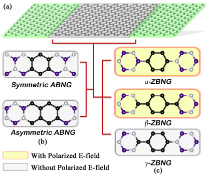
The possible BNG structures are illustrated in Fig. 1. Similar to GNR, the graphene ribbon sandwiched by BN can also be either armchair or zigzag, denoting here as ABNG and ZBNG, respectively. As shown in Fig. 1, the ABNG can be further categorized into symmetric (s-ABNG) and asymmetric (a-ABNG), depending on the exhibition of a mirror symmetry. The interfaces in both structures are charge neutral, therefore no electric field will be built up in them. Because zigzag GNR is the one that possesses peculiar edge states, we will focus our study at ZBNGs. There are two major configurations for ZBNG, distinguished by the fact that the BN and GNR atoms at the interface are connected by one bond (-ZBNG) or by two bonds (-ZBNG). While comparing the total energy, we find that -ZBNG is more stable; its energy is 93.57 meV per atom lower than that of -ZBNG. In both cases, the interfaces are either B-C or N-C and therefore are charged. The charged interface will naturally impose an electric field in the GNR region. In order to compare the ZBNG with large intrinsic polarization field, we also construct a -ZBNG, in which the interfaces consist of only N-C bonds. Therefore, the two interfaces are equally charged and no electric field will be induced.
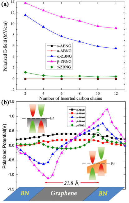
We first examine the strength of the intrinsic electric field in the BNG QWs. Fig. 2 presents the profiles of the electrostatic potentials in the four different edge configurations of BNGs. The profiles for the s-ABNG and a-ABNG are quite flat, consistent to the fact that there is no polarization field as the interfaces of the two structures are neutral. The variations of the profiles are from the small charge redistribution among the center and the edge regions of BN and GNR. In sharp contrast to ABNG, both - and -ZBNGs exhibit very large potential change between the two BN-GNR interfaces, which is a direct result of the polarization field from interface charges. For a GNR region of 21.8 Å (including 12 zigzag or armchair C-C chains), we found that the corresponding electric field are as large as 6.04 MV/cm and 10.24 MV/cm for - and - ZBNGs, respectively. This is much larger than the critical strength required for inducing half metallic state in GNRs. Furthermore, there is no monotonic electric field in graphene region of -ZBNG, which is expected. The large variation of the potential profile is due to the large charge transfer from the interface region to graphene and BN regions.

The top and side views of the spatial spin distributions in planar supercells are illustrated in Fig. 3. For ABNGs, the results are consistent with the fact that there is no edge states for armchair GNRs. However, the spin distributions are different for s- and a-ABNGs. For s-ABNG, the up-spin and down-spin densities distributed uniformly through out the supercell; whereas in a-ABNG, the GNR regions shows neither spin-up nor spin-down density, indicating non-magnetic states. We also calculated the band structures and found that both s-ABNG and a-ABNG exhibit large direct band gaps locating at point [Fig. 4(a) and (b)]. This is consistent to the existence of sizable gaps in armchair GNRs. The calculations also show that the bands of the two spin channels overlap with each other. Hexagonal BN has a much larger gap than GNR, and the band edge states are in the gap of BN. Therefore, both s-ABNG and a-ABNG are nonmagnetic and forms type one QW.

In contrast to ABNGs, the spin densities are highly localized around the interfaces for both - and ZBNGs. This is due to the fact that the spin polarization mainly happens to the edge states in the zigzag GNR region in ZBNG. For -ZBNG, the spins oriented in opposite directions at the two opposite interfaces. The band structure [Fig. 4(c)] further reveals that the -ZBNG is half metallic, since its spin-up channel is metallic and spin-down channel is semiconducting with a gap of 0.193 eV. The mechanism of this induced half metallicity is the same to the half metallicity in zigzag GNR, except that in ZBNG, the electric field is intrinsically induced by charge accumulation. The exceedingly large electric field from the interface charges allows the realization of half metallicity for a very narrow graphene region in ZBNG. While assuming that the accumulation of opposite charge on each interface does not change with the width of graphene region, we can estimate that -ZBNG containing up to 16 number of C-C zigzag chains (29.2 Å of graphene region) or ZBNG containing up to 32 number of C-C zigzag chains (60 Å of graphene region) should be already be half metallic.
For -ZBNG, we found that spin density only localized at the right interface and is spin up, which is distinctively different to -ZBNG. Noticing that the polarization field is larger in -ZBNG than in -ZBNG, we think the reason os that the strong electric field induces large charge transfer from left to the right side and the edge state at the left side is no long occupied. -ZBNG show large spin distribution at both left and right sides and with opposite orientations. However, the band structure shows that it remains semiconducting in both spin-up and spin-down channels (see Fig. 3(e)).
In conclusion, we propose an approach to achieve two dimensional half-metallic systems based on graphene and hexagonal BN lateral heterostructures. We demonstrate that the large polarization field originated from the interface charge accumulation can drive the zigzag graphene ribbons sandwiched between hBN into half metallic state in which the two spin channel locate at the opposite interfaces. The advantage of the intrinsic electric field is the avoidance of applying exceedingly large electric field at nanoscale. Considering the recent progress in fabricating BN-Graphene heterstructures, it is reasonable to expect the half metallic graphene can be observed experimentally using our proposed design.
References
- (1) B. D. Gates, Science 323, 1566 (2009).
- (2) R. J. Hamers, Nature 412, 489 (2001).
- (3) A. K. Geim, Rev. Mod. Phys. 83, 851 (2011).
- (4) K. S. Novoselov, Rev. Mod. Phys. 83, 837 (2011).
- (5) K. Mak, C. Lee, J. Hone, J. Shan, and T. F. Heinz, Phys. Rev. Lett. 105, 136805 (2010).
- (6) B. Radisavljevic, A. Radenovic, J. Brivio, V. Giacometti, and A. Kis, Nature Nanotech. 6, 147 (2011).
- (7) C. Jin, F. Lin, K. Suenaga, and S. Iijima, Phys. Rev. Lett. 102, 195505 (2009).
- (8) M. Xu, T. Lian, M. Shi, and H. Chen, Chem. Rev. 113, 3766 (2013).
- (9) A. H. Castro Neto, F. Guinea, N. M. R. Peres, K. S. Novoselov, and A. K. Geim, Rev. Mod. Phys. 81, 109 (2009).
- (10) S. Das Sarma, S. Adam, E. H. Hwang, and E. Rossi, Rev. Mod. Phys. 83, 407 (2011).
- (11) N. M. R. Peres, Rev. Mod. Phys. 82, 2673 (2010).
- (12) F. Xia, T. Mueller, Y. Lin, A. Valdes-Garcia and P. Avouris, Nature Nanotechnology 4, 839 (2009).
- (13) C. W. J. Beenakker, Rev. Mod. Phys. 80, 1337 (2008).
- (14) Zhang, Y. Tan, H. L. Stormer and P. Kim, Nature 438, 201 (2005).
- (15) K. S. Novoselov, A. K. Geim, S. V. Morozov, et al., Nature 438, 197 (2005).
- (16) D. Xiao, G. Liu, W. Feng, X. Xu and W. Yao, Phys. Rev. Lett. 108, 196802 (2012).
- (17) A. K. Geim and I. V. Grigorieva, Nature 499, 419 (2013).
- (18) B. Hunt, J. D. Sanchez-Yamagishi, A. F. Young, et al., Science 340, 1427 (2013).
- (19) K. S. Novoselov, V. I. Fal’ko, P. R. Gellert, M. G. Schwab and K. Kim, Nature 490, 192 (2012).
- (20) C. R. Dean, A. F. Young, I. Meric, et al., Nature Nanotech. 5, 722 (2010).
- (21) L. A. Ponomarenko, A. K. Geim, A. A. Zhukov, et al., Nature Phys. 7, 958 (2011).
- (22) M. Levendorf, C. Kim, L. Brown, P. Huang, et al., Nature 488, 627 (2012).
- (23) Z. Liu, L. Ma, G. Shi and P. Ajayan, et al., Nature Nanotech. 8, 119 (2013).
- (24) C. L. Kane, and E. J. Mele, Phys. Rev. Lett. 95, 226801 (2005).
- (25) D. Huertas-Hernando, F. Guinea, and A. Brataas, Phys. Rev. B 74, 155426 (2006).
- (26) Hongki Min, J. E. Hill, N. A. Sinitsyn, et al., Phys. Rev. B 74, 165310 (2006).
- (27) N. Tombros, C. Jozsa, M. Popinciuc, H. T. Jonkman, and B. J. van Wees, Nature 448, 571 (2007).
- (28) N. Tombros, S. Tanabe, A. Veligura, et al., Phys. Rev. Lett. 101, 046601 (2008); D. Huertas-Hernando, F. Guinea, and A. Brataas, Phys. Rev. Lett. 103, 146801 (2009); C. Ertler, S. Konschuh, M. Gmitra, and J. Fabian, Phys. Rev. B 80, 041405(R) (2009).
- (29) F. Zhai, and Kai Chang, Phys. Rev. B 77 113409 (2008); W. Han, K. Pi, K. M. McCreary, et al., Phys. Rev. Lett. 105, 167202 (2010); C. Weeks, J. Hu, J. Alicea, M. Franz, and R. Wu, Phys. Rev. X 1, 021001 (2011).
- (30) B. Trauzettel, D. V. Bulaev, D. Loss, and G. Burkard, Nature Phys. 3, 192 (2007).
- (31) O. V. Yazyev, Rep. Prog. Phys. 73, 056501 (2010).
- (32) J. J. Zhu, D. X. Yao, S. C. Zhang, and K. Chang, Phys. Rev. Lett. 106, 097201 (2011); D. A. Abanin, and D. A. Pesin, Phys. Rev. Lett. 106, 136802 (2011).
- (33) D. Pesin, and A. H. Macdonald, Nature Mater. 11, 409 (2012).
- (34) Y. W. Son, M. L. Cohen, and S. G. Louie, Nature. 444, 347 (2006).
- (35) G. Kresse and J. Furthmuller, Phys. Rev. B 54, 11169 (1996).
- (36) P. E. Blöchl, Phys. Rev. B 50, 17953 (1994).