Wave function description of conductance mapping for quantum Hall electron interferometer
Abstract
Scanning gate microscopy of quantum point contacts (QPC) in the integer quantum Hall regime is considered in terms of the scattering wave functions with a finite-difference implementation of the quantum transmitting boundary approach. Conductance () maps for a clean QPC as well as for a system including an antidot within the constriction are evaluated. The step-like locally flat maps for clean QPCs turn into circular resonances that are reentrant in external magnetic field when the antidot is introduced to the constriction. The current circulation around the antidot and the spacing of the resonances at the magnetic field scale react to the probe approaching the QPC. The calculated maps with a rigid but soft antidot potential reproduce the features detected recently in the electron interferometer [F. Martins et al. Nature Sci. Rep. 3, 1416 (2013)].
I Introduction
Transport properties of devices based on two-dimensional electron gas in the integer quantum Hall regime are determined by uncompensated currents that are carried by the edges of the sample.Martin The edge states have a very large coherence length Martin and they can be used for construction of electron interferometers.halperin82 ; alphenaar92 Each of the edges carry the current in a single direction only and the backscattering bu at high magnetic field requires electron transfer from one edge to the other across the bulk of the sample. The interedge tunneling paths can be opened at constrictions (quantum point contacts QPCs) which are intentionally introduced to the channel. A pair of QPCs with an internal cavity ku1 form a setup which is referred to as quantum Hall,rosenow ; hackens ; qh2 electronic Fabry-Pérot fphalperin ; fpcz ; McClure or Aharonov-Bohm (AB) interferometer.zozu1 ; caminoprb ; caminoprl The latter reference is due to the periodicity of conductance () in external magnetic field for the currents following the edges of the cavity. A similar interference mechanism and periodic behavior is found for an antidot introduced between the edges of the samplezozuantidot ; hackens ; anti1 ; anti2 ; anti3 ; anti4 ; anti5 ; anticz with electron currents encircling the antidot.
At low magnetic field the electron currents passing through a quantum point contact can be mappedqpc0 ; qpc1 ; qpc2 ; qpc4 ; qpc8 by the scanning gate microscopy sgmr which measures conductance as functions of the position of the atomic force microscope tip moving above the sample. The charged tip is capacitively coupled to the electron gas and modifies the local potential landscape. In particular a clear semi-classical magnetic focusing wff of electron currents at a field of a fraction of Tesla was observed. The magnetic fields of the order of mT lift the interference pattern of maps of QPC that appear according to the weak localization mechanism.paradiso At higher magnetic fields, within the quantum Hall regime the currents evade a direct mapping bypassing any potential perturbations introduced by the tip. The conductance in the quantum Hall regime can still be affected by the tip when it enhances the inter-edge tunnel coupling,edge1 ; edge3 depopulate the edge states within QPC,edge2 or allow for selective control of individual edge channels.paradiso
Scanning gate microscopy hackens ; qh2 was used for detection of the charging effects fpcz ; edgc ; qpc6cz of the Coulomb island in the interferometer including an intentionally introduced antidot. Recently,martinsglowna a spontaneous formation of an interferometer with a quantum Hall island (QHI) located inside a quantum point contact was demonstrated by the scanning gate microscopy. Simulations of the coherent transport in similar conditions are the purpose of the present work. To the best of our knowledge we provide the first wave function description of the scanning gate microscopy mapping of the coherent flow across the electron interferometer. The QHI is modeled as an antidot with a fixed potential. We discuss formation of current loops around the QHI which is reentrant in function of the magnetic field. We describe perturbation to the current flow pattern introduced by the tip and the consequences of bridging the edge currents by the tip for conductance. The present numerical simulations reproduce the step-like character of experimental edge2 ; paradiso ; paradiso2 integer quantum Hall maps for clean QPCs with flat minima near the QPCs and no distinct features for the tip outside of the QPC. Calculations for the electron interferometer reproduce the characteristics of experimental SGM maps,martinsglowna including the circular form of oscillations in the map, the shifts of resonant lines to lower values of by the repulsive tip as well as the reduction of the periodicity for the tip approaching the QHI. We demonstrate that the latter occurs only when the potential of the QHI potential has a soft profile.
Below we discuss the periodicity of the conductance oscillations. The early experiments ku1 ; anti1 on electron interferometers in the integer quantum Hall regime detected the Aharonov-Bohm periodicity with period , where is the flux quantum and is the area encircled by the currents. Subsequent studies caminoprl ; goldman14 reported fractional periodicity with , where is the number of edge modes fully transmitted across the sample. The fractional periodicity of AB conductance oscillations in electron interferometers are explained as due to the electron-electron interaction.rosenow The interaction effects leading to fractional periodicity are outside the range of mean field descriptionzozu1 ; zozuantidot which reproduces the period. The present calculation neglects the electron-electron interaction and in consequence the integer periodicity is found for any . We focus on the qualitative changes of the AB period that are due to the presence of the tip which are independent of .
II Model
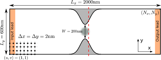

We consider a wide channel with a narrowing that is presented in Fig. 1. The channel has a width of nm that is reduced to 200 nm within the QPC. We assume that the narrowing has a Gaussian shape (aspect ratio is preserved in Fig. 1). The length of the computational box is nm.
The Fermi level electron within the system is described by a two-dimensional effective-mass Schrödinger equation
| (1) |
with the total potential , where is the confinement potential (we assume an infinite potential outside the channel and zero in the inside), is the tip potential and is the potential that models the quantum Hall island within the QPC. We consider a GaAs system with the effective electron band mass . The spin Zeeman effect for of the order of 1 T is still weak in GaAs and is neglected in the calculations.
The original potential of the tip as seen by the two-dimensional electron gas is of the Coulomb form. This potential is screened by deformation of the gas.Szafran11 In consequence the potential as seen by the Fermi level electrons is short-range. Our previous Schrödinger-Poisson calculations Szafran11 ; chwiej13 ; kolasinski13 indicated that the effective tip potential is close to Lorentzian with the width of the order of the distance between the tip and the electron gas. Accordingly, in this paper we use the Lorentz model of the potential
| (2) |
for the tip localized above point . We use nm for the width of the tip potential. The potential of the quantum Hall island is also taken in the Lorentz form
| (3) |
we assume that the QHI is located in the center of the constriction (see Fig. 1) with nm and .
We choose the Lorentz gauge for the uniform magnetic field applied perpendicular to the plane of confinement. The brown areas at the ends of the computational box in Fig. 1 denote the asymptotic regions where the boundary conditions are introduced. The calculation method applied here is a variant of the one used previously in Ref. Szafran11, . We use the gauge-invariant kinetic-energy discretization,Governale which leads to the following finite difference equation
| (4) | |||||
where , and ). For the considered magnetic fields and Fermi wave vectors, convergent results are obtained for nm.
Equation (4) defines a set of linear equations for the wave function in the interior of the computational box. The boundary conditions for the scattering problem are set in the following way. In the leads far away from the QPC and the tip potential, the confinement potential is independent of , i.e. , thus we can write the asymptotic Hamiltonian eigenfunctions as superpositions of plane waves multiplied by transverse modes . Far away from the scattering region – beyond the range of the evanescent modes – the wave function takes the form Datta
| (5) |
where is the number of subbands at the Fermi level, is the real wave vector, [] represents the -th incoming (backscattered) transverse mode. The transverse modes are found by solving the eigenproblem for the homogeneous lead.Szafran11 The coefficients and correspond to the incoming and the outgoing amplitudes, respectively. At the output lead we can write the solution in the form of superposition of outgoing modes
| (6) |
where is the amplitude of outgoing mode . The method applied in Refs. Szafran11, ; chwiej13, ; kolasinski13, used an iterative scheme for evaluation of the scattering amplitudes. Here we get rid of the iteration employing the quantum transmitting boundary (QTB) which was originally developed Lent90 ; Lent94 for the finite element method. Here we adapt QTB for the finite difference method. The details of the present calculation are given in the Appendix. A similar procedure has been applied recently in Ref. Huang12, for the current flow through ballistic nanodevices but in the absence of magnetic field.
After solution of the quantum scattering problem we evaluate the conductance by the Landauer-Büttiker formula
| (7) |
where is the transmission probability of the ’th mode incident from the input lead. The transmission for each incoming mode is calculated in the following way. For a given incoming mode we set the incoming amplitudes to , where . We solve the Schrödinger equation (4) with transmitting boundary conditions (see Appendix). Then, we calculate incoming and outgoing amplitudes (Appendix). Finally, the transmission probability is calculated from the probability current fluxes
| (8) |
where stands for the wave vector of the ’th incoming mode and the expression corresponds to the probability flux of a given mode (with ).
III Results
III.1 maps for a clean QPC
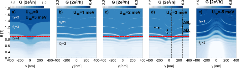
Figure 2(a) demonstrates the transfer probability summed over the subbands [Eq. (7)] as a function of the magnetic field and the Fermi energy . The function exhibits a step-like behavior with reduction of the number of the transport modes with increasing or lowering . The results of Fig. 2(a) are obtained from solution to the scattering problem involving subbands in the leads – see Fig. 2(b) which appear at the Fermi level for a given . For the further discussion we choose Fermi energy equal to meV.
The map obtained for T for the clean QPC is presented in Fig. 3(a). The conductance is reduced from to when the tip approaches the area of the QPC. Note, that when the tip is outside the QPC the map ignores its presence. The flat minimum of within the QPC and the insensitiveness of the map to the position of the tip when its outside the constriction is a characteristic feature of experimental maps obtained in SGM imaging of the edge states in QPCs – see Ref. edge2, of Ref. paradiso, [Fig. 4]. Note that in contrast to the integer quantum Hall regime, for the maps collected from the outside of the QPC contain fine details with resolved branches qpc1 ; paradiso as well as interference fringes qpc4 involving backscattering by the tip. For high the backscattering is only allowed for the tip forming bridges between the conducting sample edges, hence the flat region of the map outside the QPC.
Figure 4(a) shows the conductance for the tip scanning across the channel close to QPC along the red dashed line in Fig. 1 with varying magnetic field. In the absence of the tip the dependence has a step-like character [see Fig. 2(a)] in consistence with the experimental results of Ref. edge2, [Fig. 2(f)] and the ones of Ref. paradiso, [Fig. 4] and Ref. paradiso2, [Fig. 1(a)]. When the repulsive tip approaches the axis of the QPC () it enhances the backscattering and induces shifts of steps to lower values of . The experimental result for the equivalent measurement with QHI inside the constriction [Fig. 2(a) of Ref. martinsglowna, ] exhibits oscillations of instead of steps that appear in the result of Fig. 2(a).

III.2 maps for the interferometer
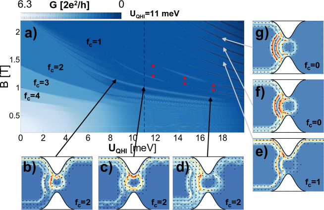
In search for the oscillatory behavior of conductance in function of the tip position we have introduced a local potential maximum to the center of the QPC in order to simulate the quantum Hall island martinsglowna with radius nm [see Eq. (3)]. The results for the transfer probability as a function of the magnetic field and the height of the QHI potential perturbation are given in Fig. 5. For low an increase of monotonically reduces the conductance. However, at higher oscillations of conductance appear. The period of these oscillations decreases with (see the red arrows), which suggests that the resonances correspond to currents circulating around the QHI with area increasing with the value of the local potential maximum. The currents in the selected locations of the diagram were presented in Fig. 5(b-g). In all the plots we find that the current approaches the QPC along the upper edge and is partially backscattered to the lower one. The transmitted current stays close to the upper edge. The area of the QHI is surrounded by an anticlockwise current with the electron density pushed to the left of the current direction in consistence with the classical Lorentz force orientation.szepl We find that the loops of current are fully developed for both resonances [Fig. 5(b-d)] and antiresonances [5(g,f)]. Outside the resonances and antiresonances the current vortex is weak [Fig. 5(e)]. We conclude that the presence of a potential defect inside the QPC leads to formation of closed current loops which is reentrant in function of for values of the magnetic field which are more or less periodically spaced. The current loops are coupled to the edge currents, hence the periodic features of conductance. For the further discussion we fix meV for which for up to 2.2 T.
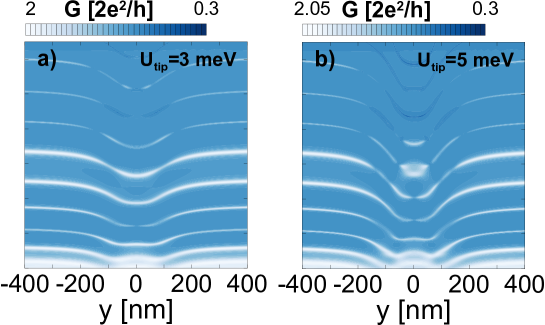
The maps obtained for T for the QHI present inside the QPC are displayed in Fig. 3(b-d). Instead of a central flat minimum of conductance found for the clean QPC [Fig. 3(a)] a resonant ring localized around the QHI defect is detected in agreement with the experimental results.martinsglowna The radius of the ring increases with .
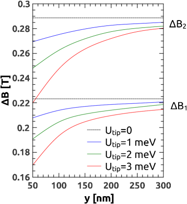
Figures 4(b-d) show scans of conductance along the line at a side of the QPC [see Fig. 1] for the increasing value of the tip potential. Already for the tip outside the channel (=400 nm), the conductance exhibits peaks which reappear nearly periodically as functions of [Fig. 5]. The repulsive tip changes the position of the resonances shifting them to lower magnetic field [Fig. 4(b-d)] in accordance with the experiment.martinsglowna . An opposite shift is found for the attractive tip [Fig.4(e)].
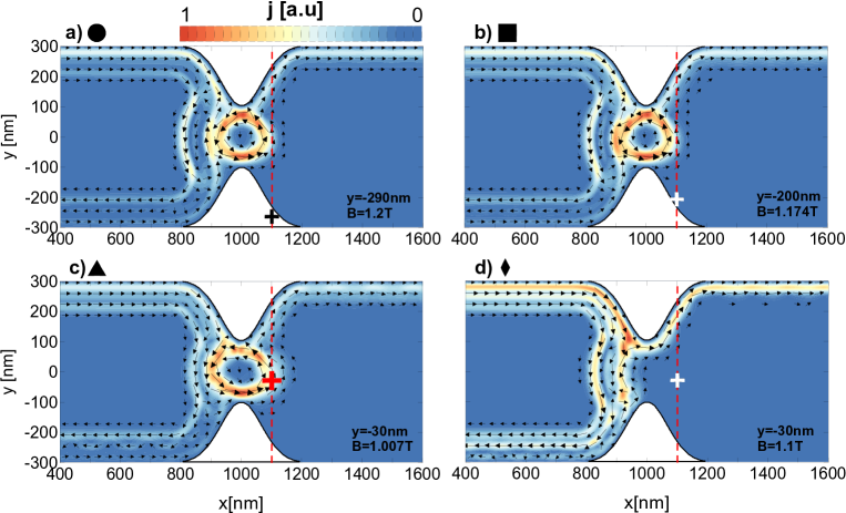
In Fig. 6 we plotted the current distribution for three points following the resonance of Fig. 4(d) that are marked by () and one point () outside the resonance [Fig. 4(e)]. The resonances are related to the interference with current circulating around the QHI. The repulsive tip potential increases the area encircled by the current when placed near the QHI [cf. Fig. 7(a) and Fig. 7(c)]. In consequence, we find that the period of the oscillations is reduced [see Fig. 7] when the tip is near QPC. Note, that for fixed the tip even when far from the center of the QPC destroys the resonant current loop while moving along the straight line (note the radial form of map of Fig. 3). In the discussed plots of Fig. 5(b-f) the values of had to be changed to follow the resonance. Moreover, for the attractive tip [Fig. 4(e)] the spacing between the resonances increases when tip gets close to the center of the QPC, indicating that the area encircled by the current is decreased. The present calculations confirm the interpretation of Ref. martinsglowna, that the reduced period of oscillations for the repulsive tip is a signature of the presence of QHI inside the QPC. Note, that the spacings between values – already in the absence of the tip are not exactly equal (see Fig. 7 for ), which results from the softness of the assumed QHI potential. For the current circulates counter-clockwise around the QHI [see Fig. 5(b-g)]. The Lorentz force pushes the electron density to the left of the current. For higher magnetic field the shift of the electron density to the center of QHI is stronger, hence the reduced area of the loop [cf. Fig. 5(b) and (d)] and the increased Aharonov-Bohm period.
The change of the Aharonov-Bohm period with the presence of the tip results from superposition of the two potentials: the one of the defect forming the QPC and the tip potential. We find that in order for this superposition to be effective in the modulation of the period the potential of the defect needs to be soft. We have performed calculations for a hard-wall QHI potential simulated by
| (9) |
For the purpose of the hard-wall simulation we adopted meV exceeding by 4 meV the Fermi energy, and nm. The results for the scan along the path marked in Fig. 1 by the dashed line are given in Fig. 8. In contrast to the results with the soft QHI potential of Fig. 4 we notice that i) in the absence of the tip ( nm) the subsequent resonances at the scale are spaced by periods which change with the magnetic field much more slowly than for the soft QHI defect and ii) the presence of the tip shifts the position of the resonances but does not change their spacing significantly as it was the case for the soft QHI defect.
IV Summary and Conclusions
We have simulated scanning gate microscopy mapping of conductance of both a clean QPC and the one turned into an electron interferometer by a local maximum of the potential landscape in the integer quantum Hall regime. We have solved the quantum scattering problem as given by the Schrödinger equation using a direct finite difference approach with an implementation of the quantum transmitting boundary method. We have described the stepwise reduction of conductance that is due to the tip for clean QPC as well as formation of resonant current loops around the potential defect when introduced to the constriction. We found that the repulsive tip reduces the period of the Aharonov-Bohm-like conductance oscillations for the interferometers. We demonstrated that the periodicity of AB oscillations reacts to the tip only when the potential defect within QPC has a soft character. The presented results for the conductance maps are consistent with the recent experimental results for both clean QPCs and the electron interferometer.
Appendix
This Appendix contains the details of the implementation of the quantum transmitting boundary method for the finite difference approach. After Refs. Lent90, ; Lent94, we multiply both sides of Eq. (5) by a complex conjugate of the m-th outgoing transverse mode , then we integrate both sides along the channel, putting
| (10) |
where is a standard inner product calculated for the transverse wave function across the channel, here written in finite difference formalism. Equation (10) can be written as system of -th linear equations for outgoing amplitudes
| (11) |
with , , , , and .
Note, that the different lateral modes are not orthogonal in presence of the external magnetic field,Datta and thus and its inverse matrix are not diagonal. We use Eq. (11) to express vector in terms of the incident amplitudes
with
| (12) |
In order to apply the boundary conditions for Eq. (4), we calculate the derivative of Eq. (5) at () using the standard central finite difference formula for first order derivative
| (13) |
where
Now we put the Eq. (12) to the Eq. (13), where we also use the formula for inner product
we get
where
From (Eq. Appendix) we get
which we put into the Schrödinger equation (4) in order to apply boundary conditions for nodes with
Since , we get
which is the final formula for the boundary condition for the input lead. Using Eq. (6) and choosing the coordinate frame in which at nodes with we get
| (14) |
The same as for the input lead one can show that the boundary condition at the output lead is given by formula
with
References
- (1) R.J. Haug, Semicond. Sci. Technol. 8, 131 (1993).
- (2) B.I. Halperin, Phys. Rev. B 25, 2185 (1982).
- (3) B.W. Alphenaar, A.A.M. Staring, H. van Houten, M.A.A. Mabesoone, O.J.A. Buyk, and C.T Foxon, Phys. Rev. B 46, R7236 (1992).
- (4) M. Büttiker, Phys. Rev. B 38, 9375 (1988).
- (5) B.J. van Wees, L.P. Kouwenhoven, C.J.P.M. Harmans, J.G. Williamson, C.E. Timmering, M.E.I. Broekaart, C.T. Foxon, and J.J. Harris, Phys. Rev. Lett. 62, 2523 (1989).
- (6) B. Rosenow, and B.I. Halperin, Phys. Rev. Lett. 98, 106801 (2007).
- (7) B. Hackens, F. Martins, S. Faniel, C.A. Dutu, H. Sellier, S. Huant, M. Pala, L. Desplanque, X. Wallart, and V. Bayot, Nature Communications, 1, 39 (2010).
- (8) F. Martins, S. Faniel, B. Rosenow, M.G. Pala, H. Sellier, S. Huant, L. Desplanque, X. Wallart, V. Bayot, B. Hackens, New J. Phys. 15, 013049 (2013).
- (9) B.I. Halperin, A. Stern, I. Neder, and B. Rosenow, Phys. Rev. B 83, 155440 (2011).
- (10) Y. Zhang, D.T. McClure, E.M. Levenson-Falk, C.M. Marcus, L.N. Pfeiffer, and K.W. West, Phys. Rev. B 79, R241304 (2009).
- (11) D.T. McClure, Y. Zhang, B. Rosenow, E.M. Levenson-Falk, C.M. Marcus, L.N. Pfeiffer, and K.W. West, Phys. Rev. Lett. 103, 206806 (2009).
- (12) S. Ihnatsenka, and I.V. Zozoulenko, Phys. Rev. B 77, 235304 (2008).
- (13) F.E. Camino, W. Zhou, and V.J. Goldman, Phys. Rev. B 72, 155313 (2005); 76, 155305 (2007).
- (14) F.E. Camino, W. Zhou, and V.J. Goldman, Phys. Rev. Lett. 95, 246802 (2005).
- (15) V.J. Goldman, J. Liu, and A. Zaslavsky, Phys. Rev. B 77, 115328 (2008).
- (16) S. Ihnatsenka, I.V. Zozoulenko, and G. Kirczenow, Phys. Rev. B 80, 115303 (2009).
- (17) S.W. Hwang, J.A. Simmons, D.C. Tsui, and M. Shayegan, Phys. Rev. B 44, 13497 (1991).
- (18) C.J.B. Ford, P.J. Simson, I. Zailer, D.R. Mace, M. Yosefin, M. Pepper, D.A. Ritchie, J.E.F. Frost, M.P. Grimshaw, and G.A.C. Jones, Phys. Rev. B 49, 17456 (1994).
- (19) A.S. Sachrajda, Y. Feng, R.P. Taylor, G. Kirczenow, L. Henning, J. Wang, P. Zawadzki, and P.T. Coleridge, Phys. Rev. B 50, 10856 (1994).
- (20) G. Kirczenow, A.S. Sachrajda, Y. Feng, R.P. Taylor, L. Henning, J. Wang, P. Zawadzki, and P.T. Coleridge, Phys. Rev. Lett. 72, 2069 (1994).
- (21) V.J. Goldman, J.Liu, and A. Zaslavsky, Phys. Rev. B 71, 153303 (2005).
- (22) M. Kataoka, C.J.B. Ford, G. Faini, D. Mailly, M.Y. Simmons, D.R. Mace, C.T. Liang, and D.A. Ritchie, Phys. Rev. Lett. 83, 160 (1999).
- (23) R. Crook, C.G. Smith, M.Y Simmons, and D.A. Ritchie, Phys. Rev. B 62, 5174 (2000).
- (24) M.A. Topinka, B.J. LeRoy, S.E.J. Shaw, E.J. Heller, R.M. Westervelt, K.D. Maranowski, and A.C. Gossard, Science 289, 2323 (2000).
- (25) M.A. Topinka, B.J. LeRoy, R.M. Westervelt, S.E.J. Shaw, R. Fleischmann, E.J. Heller, K.D. Maranowski, A.C. Gossard, Nature,410, 183 ( 2001).
- (26) M.P. Jura, M.A. Topinka, L. Urban, A. Yazdani, H. Shtrikman, L.N. Pfeiffer, K.W. West, and D. Goldhaber-Gordon D, Nat. Phys.3, 841 (2007).
- (27) A.A. Kozikov, D. Weinmann, C. Rössler, T. Ihn, K. Ensslin, C. Reichl, and W. Wegscheider, New J. Phys. 15, 083005 (2009).
- (28) H. Sellier, B. Hackens, M.G. Pala, F. Martins, S. Baltazar, X. Wallart, L. Desplanque, V. Bayot, and S. Huant, Sem. Sci. Tech. 26, 064008 (2011); D.K. Ferry, A.M. Burke, R. Akis, R. Brunner, T.E. Day, R. Meisels, F. Kuchar, J.P. Bird, and B.R. Bennett, Sem. Sci. Tech. 26, 043001 (2011).
- (29) K.E. Aidala, R.E. Parott, T. Kramer, E.J. Heller, R.M. Westervelt, M.P. Hanson, and A.C. Gossard, Nat. Phys. 3, 464 (2007).
- (30) N. Paradiso, S. Heun, S.Roddaro, L.N. Pfeiffer, K.W. West, L. Sorba, G. Biasiol, F. Beltram, Physica E 42, 1038 (2010).
- (31) J. Rychen, T. Vančura, K. Ensslin, W. Wegscheider, M. Bichler, Physica E 13, 671 (2002).
- (32) S. Kičin, A.Pioda, T. Ihn, K. Ensslin, D.D. Driscoll, and A.C. Gossard, Physica E 21, 708 (2004).
- (33) N. Aoki, C.R. Cunha, R. Akis, D.K. Ferry, Y. Ochiai, Phys. Rev. B 72, 155327 (2005).
- (34) T. Ihn, J. Rychen, T. Vancura, K. Ensslin, W. Wegscheider, M. Bichler, Physica E 13, 671 (2002).
- (35) A. Pioda, S. Kicin, D. Brunner, T. Ihn, M. Sigrist, K. Ensslin ,M. Reinwald, and W. Wegscheider, Phys. Rev. B 75, 045433 (2007).
- (36) F. Martins, S. Faniel, B. Rosenow, H. Sellier, S. Huant, M. G. Pala, L. Desplanque, X. Wallart, V. Bayot, and B. Hackens, Nature Scientific Reports 3, 1416 (2013).
- (37) N. Paradiso, S. Heun, S. Roddaro, L. Sorba, F. Beltram, G. Biasiol, L. N. Pfeiffer, and K. W. West, Phys. Rev. Lett. 108, 246801 (2012).
- (38) B. Szafran, Phys. Rev. B 84 075336 (2011).
- (39) T. Chwiej, and B. Szafran, Phys. Rev. B 87, 085302 (2013).
- (40) K. Kolasiński, and B. Szafran, Phys. Rev. B 88, 165306 (2013).
- (41) M. Governale, and C. Ungarelli, Phys. Rev. B 58, 7816 (1998).
- (42) S. Datta, Electronic Transport in Mesoscopic Systems (Cambridge University Press, Cambridge, England, 1995).
- (43) D.J. Kirkner, and C.S. Lent, Journal of Applied Physics 67, 6353 (1990).
- (44) M. Leng, and C. S. Lent, Journal of Applied Physics 76, 2240 (1994).
- (45) J. Huang, C.C. Weng, T. Min, and J. Lijun, IEEE Trans. Electron Devices 59, 468 (2012).
- (46) B. Szafran and F.M. Peeters, Europhys. Lett. 70, 810 (2005).
- (47) J.W. Demmel, S.C. Eisenstat, J.R. Gilbert, X.S. Li, and J.W.H. Liu, SIAM. J. Matrix Anal. Appl. 20, 720 (1999).