Impurity-assisted tunneling magnetoresistance under weak magnetic field
Abstract
Injection of spins into semiconductors is essential for the integration of the spin functionality into conventional electronics. Insulating layers are often inserted between ferromagnetic metals and semiconductors for obtaining an efficient spin injection, and it is therefore crucial to distinguish between signatures of electrical spin injection and impurity-driven effects in the tunnel barrier. Here we demonstrate an impurity-assisted tunneling magnetoresistance effect in nonmagnetic-insulator-nonmagnetic and ferromagnetic-insulator-nonmagnetic tunnel barriers. In both cases, the effect reflects on/off switching of the tunneling current through impurity channels by the external magnetic field. The reported effect is universal for any impurity-assisted tunneling process and provides an alternative interpretation to a widely used technique that employs the same ferromagnetic electrode to inject and detect spin accumulation.
For the realization of semiconductor spintronic devices Kato_Science04 ; Nagaosa_03 ; Crooker_Science05 ; Zutic_RMP04 ; Dery_Nature07 ; Zutic_RMP04 ; Appelbaum_Nature07 ; Dery_Nature07 ; Li_PRL13 ; Sasaki_APL11 , the conductivity mismatch problem Johnson_PRB87 ; Schmidt_PRB00 ; Rashba_PRB00 ; Fert_PRB01 and the difficulty of manipulating semiconductors at the nanoscale are the main issues delaying the progress of this research field. Employing the so-called three-terminal (3T) setup and making use of a single ferromagnetic/insulator contact for both injection and detection of spin-polarized currents was a big step towards this purpose Dash_Nature09 . Due to the simplicity of the micron-sized structures employed, this setup has gained popularity in semiconductor spintronics Dash_Nature09 ; Tran_PRL09 ; Li_NatureComm11 ; Dash_PRB11 ; Aoki_PRB12 ; Jain_PRL12 ; Uemura_APL12 ; Sharma_PRB14 ; Shiogai_PRB14 ; Tinkey_arxiv14 . The Lorentzian-shaped magnetoresistance (MR) effect measured in 3T-semiconductor devices has been often attributed to spin injection on accounts of the resemblance to the celebrated Hanle effect in optical spin injection experiments Optical_Orientation . However, it has been increasingly realized that the MR reported depends much on the tunneling process and too little on the semiconductor Dash_Nature09 ; Tran_PRL09 ; Li_NatureComm11 ; Dash_PRB11 ; Aoki_PRB12 ; Jain_PRL12 ; Uemura_APL12 ; Sharma_PRB14 ; Shiogai_PRB14 ; Tinkey_arxiv14 . Furthermore, the typical junction working conditions employed for these measurements, with bias voltage settings much larger than the Zeeman energy, render the signal detection prone to subtle effects driven by impurities embedded in the tunnel barrier Song_Dery_FIN ; Tran_PRL09 .
In this Letter, we elucidate the physics behind such experiments by focusing on the tunnel barrier. Accordingly, our devices render a compact geometry with an aluminum-oxide tunnel barrier created between metallic electrodes, M1/AlOx/M2, as sketched in Fig. 1(a). The M1/AlOx/M2 devices were fabricated in-situ in a UHV electron-beam evaporation chamber with integrated shadow masks. The base pressure of the chamber is below mbar. The thickness of the top and bottom metallic electrodes, M1 and M2, ranged between 10 nm and 15 nm. To decisively probe the role of impurities in the oxide, a series of devices were fabricated with 1) O2 plasma exposure at mbar at a power ranging from around 24 to 40 W for 120 seconds to 210 seconds to minimize the impurity density, or 2) step ( from 2 to 5) deposition of a 6 Å Al layer with subsequent oxidation of 20 min at mbar of O2 pressure with no plasma. The latter method allows us to vary the density and locations of impurities Txoperena_APL13 ; Rippard_PRL02 . The area of the tunnel barrier ranges from 200275 m2 to 375555 m2. The junction resistance is measured with the typical 4-point sensing configuration shown in Fig. 1(a), and the associated MR signal is the ratio between the voltage change across the junction and the constant current between the metallic leads when an external magnetic field is applied. The total amplitude of will be called . By using metallic electrodes, we avoid the complications brought by the Schottky barrier and Fermi-level pinning when using a semiconductor Sze_Book , and we are able to establish a direct relation between the measured signals and the tunnel barrier. Moreover, we detect similar MR effects in ferromagnetic-insulator-nonmagnetic (FIN) and nonmagnetic-insulator-nonmagnetic (NIN) devices, and explain both of them by considering the magnetic-field-induced on/off switching of the tunneling current through impurities embedded in the tunnel barrier. This important finding calls for investigation of a novel effect and provides an alternative interpretation to recent 3T spin injection experiments, whose magnetoresistance has been attributed to spin accumulation on a nonmagnetic material. Although we do not rule out spin injection in our FIN devices, spin accumulation is clearly not being measured in our setup, since the measured signals are many orders of magnitude higher than those expected from the standard theory of spin diffusion and accumulation Txoperena_APL13 .
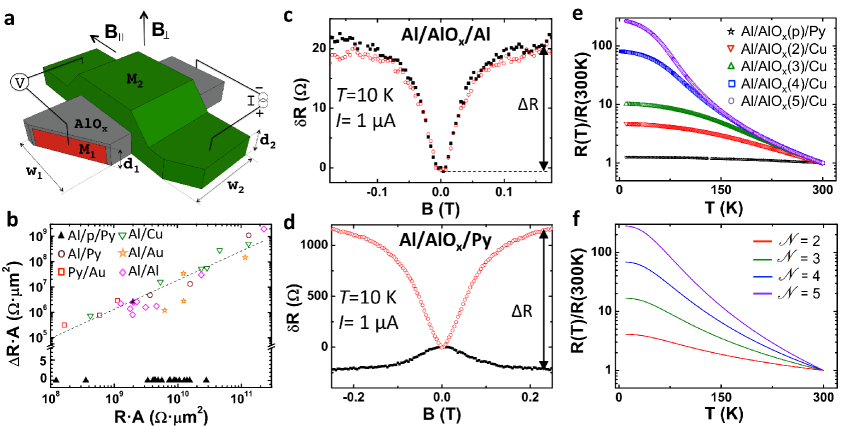
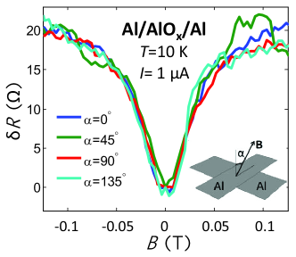
Figure 1(b) shows a compilation of the total amplitude of the MR effect multiplied by the total area of the tunnel barrier (A) for step tunnel barriers (with 2, 3, 4 and 5) with a variety of metallic electrodes, as well as Al/AlOx/Py plasma-oxidized tunnel junctions. For plasma-oxidized AlOx, M1=Al and M2=Py are used (21 devices in total); and the combinations of M1 and M2 metals for step AlOx are: M1=Al with M2=Py (3 devices), with M2=Al (9 devices), with M2=Cu (6 devices) and with M2=Au (4 devices), and M1=Py combined with M2=Au (3 devices). Excluding the vast majority of the plasma-oxidized barriers, we find a power law scaling relation between A and A, with an exponent factor of 1.19 (0.09) [dashed line in Fig. 1(b)]. In the following we focus on the results of two representative impurity-rich NIN (Al/AlOx/Al) and FIN (Al/AlOx/Py) devices whose tunnel barriers are fabricated by a three-step deposition procedure. Figure 1(c) shows of the NIN device modulated by out-of-plane () and in-plane () fields. The full width at half maximum (FWHM) of both curves is 0.065 T and the junction resistance increases with regardless of its orientation. We corroborated the isotropy of in the NIN device for more magnetic field orientations supple . Figure 1(d) shows the respective measurements in the FIN device where the FWHM is 0.134 T (0.142 T) and the resistance increases (decreases) when applying an in-plane (out-of-plane) magnetic field. Notably, the FWHM and values in our devices are comparable to the recurring values seen by 3T-FIN devices employing various insulators and N materials Dash_Nature09 ; Tran_PRL09 ; Li_NatureComm11 ; Dash_PRB11 ; Aoki_PRB12 ; Jain_PRL12 ; Uemura_APL12 ; Sharma_PRB14 ; Erve_NatureNano12 ; Han_NatureComm13 .
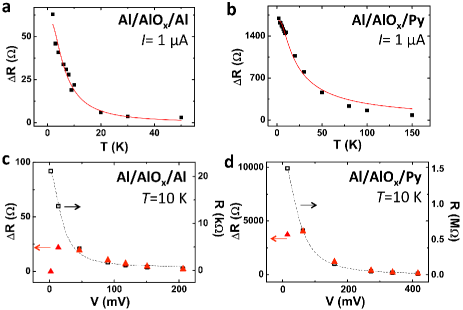
The fact that we observe a non-zero MR signal in NIN, where no spin-polarized source is present, indicates that the MR effect is governed by the oxide barriers rather than by non-equilibrium spin accumulation in N. To better understand the underlying tunnel mechanism, Fig. 1(e) shows the temperature dependence of in a series of devices with different tunnel barriers. The of the plasma-oxidized junction shows a weak temperature dependence, in agreement with direct tunneling transport Akerman_JMMM2002 . In contrast, the data corresponding to step barriers (2, 3, 4 and 5) show a stronger T dependence. This dependence can be described by acoustic phonon-assisted tunneling through impurities that dominate the conduction and should follow , where is the number of impurities assisting the tunneling event, is the Bose-Einstein distribution, and is the upper energy of acoustic phonons in the barrier. Figure 1(f) shows that for an step tunnel junction we indeed reproduce the experimental results with 17 meV Heid_PRB00 and , in agreement with the fabrication method employed. We further support the phonon-assisted tunneling picture by employing the Glazman-Matveev theory Glazman_JETP88_phonon to analyze the I-V curves supple . Confirmation that the effect is entirely impurity-driven comes from the fact that the MR effect is observed in impurity-rich step tunnel barriers while being suppressed in plasma-oxidized barriers where direct tunneling is dominant [Fig. 1(b)]. The and dependence of the MR amplitude , displayed in Fig. 2, can be explained in this framework, as will be discussed below. Figures 2(a) and 2(b) show a pronounced decrease of with for the NIN and FIN devices, respectively. Figures 2(c) and 2(d) show that, in both NIN and FIN, follows a similar voltage dependence as , except for a sharp decrease when is close to zero. We observe similar voltage dependences for different step barriers supple .
We propose a tunneling mechanism to explain the experimental findings. Using the gained information regarding tunneling across impurity chains in our devices, we classify impurities with large on-site Coulomb repulsion energy () into type A and type B classes. In type A (B), the filling energy for the first (second) electron is within the bias window Glazman_JETP88_Coulomb ; Bahlouli_PRB94 . This simple classification of the energetic levels of the localized states captures the core physics of our experiments Boero_PRL97 . Figure 3(a) shows an example when both types form an A-B chain in the tunnel barrier of a NIN junction. When electrons tunnel in the direction from A to B, this chain enables on (off) current switching in small (large) external magnetic fields. To understand this effect, we first focus on the steady-state spin configuration in the chain. Once an electron tunnels from the left bank into the type A impurity, it can be intuitively viewed as an ideal polarized source (‘one electron version of a half metal’). Due to Pauli blocking, this electron cannot hop to the second level of the type B impurity if the first level of the latter is filled with an electron of same spin orientation [see Fig. 3(a)]. The steady-state current across the chain is therefore blocked. This blockade can be lifted when the correlated spin configuration is randomized by spin interactions, which include the spin-orbit coupling Prioli_PRB95 , hyperfine coupling with the nuclear spin system Boero_PRL97 , and spin-spin exchange interactions with unpaired electrons in neighboring impurities Helman_PRL76 . Whatever is the dominant interaction, we can invoke a mean-field approximation and view this interaction as an internal magnetic field at the impurity site that competes with the external field. When the external field is much larger than the internal fields, the type A and type B impurities in the chain see similar fields and the current is Pauli blocked as explained before. In the opposite extreme of negligible external field, the blockade is lifted since the correlated spin configuration is violated by spin precession about internal fields that are likely to point in different directions on the A and B sites. This behavior is illustrated by Fig. 3(b). Although A-B impurity chain is the simplest case that supports magnetic field modulation of the current, similar modulations will also occur in longer chains containing an A-B sequence.

Next we consider FIN junctions. Due to the magnetization of F, there are two main differences compared to NIN. First, the polarized tunnel current in FIN facilitates partial blocking of the impurity-assisted current already without an external field. In NIN junctions, on the other hand, the current is unblocked without an external field due to the randomized spin configuration induced by the presence of internal fields. As will be explained below, the result is that in FIN junctions the tunnel resistance can either increase (larger blocking) or decrease (weaker blocking) depending on the magnetic field orientation with respect to the magnetization axis of F. The second difference is that chains with at least one A-B sequence are needed in order to have field modulation in NIN (where the type A impurity plays the role of ‘polarizing’ the incoming current). In case of FIN, on the other hand, a single impurity is sufficient to block the current. It can be any chain with at least one type B impurity when electrons flow from F to N (spin injection), or at least one type A impurity when electrons flow from N to F (spin extraction) Song_Dery_FIN . Current blockade is established once the spin in the lower level of the type B (A) impurity is parallel (antiparallel) to the majority spins of F in spin injection (extraction). The blockade is lifted when applying an out-of-plane field whose magnitude is much smaller than the saturation field of F. Spin precession of the electron in the lower level of the type B (A) impurity lifts the blockade since this electron can no longer keep a parallel (antiparallel) spin configuration with the majority spins of F. This physical picture explains the measured reduction in the resistance of the FIN for this field orientation [see Fig. 1(d)]. On the other hand, by applying a field parallel to the magnetization axis of F, the resistance increases since the external field impedes spin precession induced by random internal magnetic fields. Therefore, the current blocked configurations are reinforced: spins in the lower levels of type B (A) impurities are parallel (antiparallel) to the majority spins of F in injection (extraction). Such reinforcement is equivalent to the behavior of NIN junctions under a magnetic field pointing in any direction. The above discussed behavior in FIN explains the measured anisotropy in shown in Fig. 1(d). Finally, we emphasize that, details aside, the underlying physics of the MR effect is the same in both FIN and NIN junctions.
To quantify the impurity-assisted tunneling magnetoresistance effect, we describe a toy model based on the tunneling through two-impurity chains by generalizing the Anderson impurity Hamiltonian model to our tunneling case Glazman_JETP88_phonon . The steady-state current across the impurity chains are then found by invoking non-equilibrium Green function techniques and deriving master equations in the slave-boson representation Zou_PRB88 ; LeGuillou_PRB95 . The technical details are given in the supplemental material supple . The steady-state current essentially represents competition between the Zeeman terms, impurity-lead coupling ( where denotes Left/Right impurity-lead pair), and inter-impurity coupling (). These coupling terms reflect tunneling rates (via ). Solving the master equations for the particular case of the A-B impurity chain and bias setting described in Fig. 3, we obtain the following steady-state solution for the dominant contribution supple ,
| (1) |
This expression describes the magnetic-field modulated current via an A-B impurity chain, where the magnetic field dependence is manifested via the angle . For large enough external field () the effective fields in the left and right impurities are aligned (), and the current is blocked (i.e., leading to ). When is much smaller than the internal fields, on the other hand, is effectively of the order of 1/2 after averaging over the distribution of , and the current can flow. The full expression for is given in Eq. (S3) of the supplemental material supple , and in Eq. (1) above we show its simplified form in the limit that the Zeeman energy is larger than the impurity-lead and impurity-impurity couplings (’s). This limit is generally satisfied due to the random distribution of internal fields whose magnitudes and variations can readily exceed those of the weak coupling parameters. In this limit, the FWHM are determined by the characteristic amplitude of the internal fields. This explains why the stray fields due to the F/I roughness Dash_PRB11 that add to the internal fields in FIN give rise to somewhat larger FWHM values compared to NIN. It also justifies the independence of the measured FWHM values on the thickness of the tunnel barrier. Equation (1) shows a series-like resistance for the A-B chain where the negative term, , stems from the coherence between two impurities supple .
We can now recover the measured signal by noting that
| (2) |
where is the number of A-B chains with , and is the total current enabled via tunneling over impurity clusters with various sizes and on-site repulsion ’s.
All the obtained experimental results are readily understood by applying the above analysis. First, Fig. 3(c) shows a current simulation using Eq. (1) after averaging over the amplitude and orientation of the internal fields. Since the tunneling probability decays exponentially with the barrier thickness, the dominant contribution comes from equidistant impurities for which Bahlouli_PRB94 . Using this equality, we model the internal field in each of the impurities as an independent normalized Gaussian distribution whose mean and standard deviation are 20 and , respectively supple . We observe that the shape of the simulated curve is in agreement with the Lorentzian shape measured in both NIN and FIN [Figs. 1(c) and 1(d)]. Second, we explain the behavior for the NIN and FIN devices. On the one hand, we observe a stronger T dependence of the signal for NIN than for FIN [see Figs. 2(a) and 2(b)]. The origin for this behavior is that in NIN devices the blockade is effective when for both impurities on the A-B chain. By contrast, in the FIN devices, it is sufficient to have one such impurity due to the spin polarization of F, rendering less temperature dependent. Using this information, can be fitted by a typical Arrhenius law where for NIN (FIN) devices. The red lines in Figs. 2(a) and 2(b) show the dependence where the activation energy is meV for the NIN device and meV for the FIN device. The activation energy meV is associated with the threshold of small impurities to merge into larger clusters resulting in Helman_PRL76 . This scenario is compatible with our devices where apart from isolated impurities, we might also have impurities in close proximity behaving as big clusters as temperature is increased. Third, the decrease of at low bias values [Figs. 2(c) and 2(d)] is because of the vanishing number of A-B channels within the small bias window. Finally, related to that, the relative signal is a result of the small portion of A-B chains with among all cluster chains. The fact that is nearly constant comparing all devices, as shown in Fig. 1(b), is in agreement with Eq. (2).
In conclusion, the MR effect shows how the impurity-assisted tunnel resistance can be modulated by a magnetic field when the Zeeman splitting of the impurity spin states is smaller compared to the applied bias voltage. Other impurity-driven effects reported up to date, such as the Kondo effect or Coulomb correlation in resonant tunneling Gordon_Nature98 ; Ephron_PRL92 ; Xu_PRB95 , appear in the opposite regime at strong magnetic fields. This mechanism therefore promises new possibilities to explore local states in disordered materials or nanostructures. Our analysis puts NIN and FIN junctions on an equal footing, with the physical picture readily generalizable to chains with impurities in NIN (FIN) junctions. This novel magnetoresistance effect is general for any impurity-assisted tunneling process regardless of the oxide thickness or materials used. Therefore, the presented work will be used as a benchmark to spin injection experiments to any nonmagnetic material, and specially will redirect research of semiconductor spintronics, with all the implications in such a technologically relevant area.
The authors acknowledge Dr. A. Bedoya-Pinto for fruitful discussions. The work in Spain is supported by the European Union 7th Framework Programme (NMP3-SL-2011-263104-HINTS, PIRG06-GA-2009-256470 and the European Research Council Grant 257654-SPINTROS), by the Spanish Ministry of Economy under Project No. MAT2012-37638 and by the Basque Government under Project No. PI2011-1. The work in USA is supported by NRI-NSF, NSF, and DTRA Contracts No. DMR-1124601, ECCS-1231570, and HDTRA1-13-1-0013, respectively.
References
- (1) Y. K. Kato, R. C. Myers, A. C. Gossard, and D. D. Awschalom, Science 306, 1910 (2004).
- (2) S. Murakami, N. Nagaosa, and S.-C. Zhang, Science 301, 1348 (2003).
- (3) I. Zutic, J. Fabian, and S. D. Sarma, Rev. Mod. Phys. 76, 323 (2004).
- (4) H. Dery, P. Dalal, Ł. Cywiński, and L. J. Sham, Nature 447, 573 (2007).
- (5) S. A. Crooker et al., Science 309, 2191 (2005).
- (6) I. Appelbaum, B. Huang, and J. Monsma, Nature 447, 295 (2007).
- (7) P. Li, J. Li, L. Qing, H. Dery, and I. Appelbaum, Phys. Rev. Lett. 111, 257204 (2013).
- (8) T. Sasaki et al., Appl. Phys. Lett. 98, 012508 (2011).
- (9) M. Johnson and R. H. Silsbee, Phys. Rev. B 35, 4959 (1987).
- (10) G. Schmidt, D. Ferrand, L. W. Molenkamp, A. T. Filip, and B. J. van Wees, Phys. Rev. B 62, R4790 (2000).
- (11) E. I. Rashba, Phys. Rev. B 62, R16267 (2000).
- (12) A. Fert and H. Jaffres, Phys. Rev. B 64, 184420 (2001).
- (13) S. P. Dash, S. Sharma, R. S. Patel, M. P. de Jong, and R. Jansen, Nature 462, 491 (2009).
- (14) M. Tran et al., Phys. Rev. Lett. 102, 036601 (2009).
- (15) C. H. Li, O. M. G. van ’t Erve, and B. T. Jonker, Nature Commun. 2, 245 (2011).
- (16) S. P. Dash et al., Phys. Rev. B 84, 054410 (2011).
- (17) Y. Aoki et al., Phys. Rev. B 86, 081201(R) (2012).
- (18) A. Jain et al., Phys. Rev. Lett. 109, 106603 (2012).
- (19) T. Uemura, K. Kondo, J. Fujisawa, K.-I. Matsuda, and M. Yamamoto, Appl. Phys. Lett. 101, 132411 (2012).
- (20) S. Sharma et al., Phys. Rev. B 89, 075301 (2014).
- (21) J. Shiogai et al., Phys. Rev. B 89, 081307(R) (2014).
- (22) H. N. Tinkey, P. Li, and I. Appelbaum, arXiv: 1405.2297.
- (23) F. Meier and B. P. Zakharchenya, Ed., Optical Orientation (North-Holland, New York, 1984).
- (24) Y. Song and H. Dery, Phys. Rev. Lett. 113, 047205 (2014).
- (25) O. Txoperena et al., Appl. Phys. Lett. 102, 192406 (2013).
- (26) W. H. Rippard, A. C. Perrella, F. J. Albert, and R. A. Buhrman, Phys. Rev. Lett. 88, 046805 (2002).
- (27) S. M. Sze, Physics of Semiconductor Devices (Wiley, New York,1981).
- (28) See Supplemental Material at [URL will be inserted by publisher] for supporting experiments showing (a) the isotropy of the signal in NIN junctions with respect to the orientation of the magnetic field, (b) analysis of the I-V curves using the Glazmann-Matveev theory for phonon-assisted tunneling, (c) Bias dependence of the signal in NIN junctions with 3-step, 4-step and 5-step tunnel barriers. In addition, it includes the Hamiltonian model and resulting master equations along with analytical expressions for the tunnel current. It also includes simulation details for the results of Fig. 3(c), and a quantitative discussion showing the proposed MR effect can elucidate recent experimental results of FIN junctions where N is a semiconductor.
- (29) O. M. J. van ’t Erve et al., Nature Nanotechnol. 7, 737 (2012).
- (30) W. Han et al., Nature Commun. 4, 2134 (2013).
- (31) J. J. Åkerman et al., J. Magn. Magn. Mater. 240, 86-91 (2002).
- (32) R. Heid, D. Strauch, and K.-P. Bohnen, Phys. Rev. B 61, 8625 (2000).
- (33) L. I. Glazman and K. A. Matveev, Zh. Eksp. Teor. Fiz. 94, 332 (1988) [Sov. Phys. JETP 67, 1276 (1988)].
- (34) L. I. Glazman and K. A. Matveev, Pis’ma Zh. Eksp. Teor. Fiz. 48, 403 (1988) [JETP Lett. 48, 445 (1988)].
- (35) H. Bahlouli, K. A. Matveev, D. Ephron, and M. R. Beasley, Phys. Rev. B 49, 14496 (1994).
- (36) R. Prioli and J. S. Helman, Phys. Rev. B 52, 7887 (1995).
- (37) M. Boero, A. Pasquarello, J. Sarnthein, and R. Car, Phys. Rev. Lett. 78, 887 (1997).
- (38) J. S. Helman and B. Abeles, Phys. Rev. Lett. 37, 1429 (1976).
- (39) Z. Zou and P. W. Anderson, Phys. Rev. B 37, 627(R) (1988).
- (40) J. C. Le Guillou and E. Ragoucy, Phys. Rev. B 52, 2403 (1995).
- (41) D. Goldhaber-Gordon, et al., Nature 391, 156 (1998).
- (42) D. Ephron, Y. Xu, and M. R. Beasley, Phys. Rev. Lett. 69, 3112 (1992).
- (43) Y. Xu, D. Ephron, and M. R. Beasley, Phys. Rev. B 52, 2843 (1995).
Supplemental Material for “Universal impurity-assisted tunneling
magnetoresistance under weak magnetic field”
Oihana Txoperena, Yang Song, Lan Qing, Marco Gobbi,
Luis E. Hueso, Hanan Dery, Fèlix Casanova
Additional experimental results and discussion
In Fig. S1, we show two additional magnetic field (B) directions applied on the representative NIN device. We observe no correlation between the MR signals and the field directions.
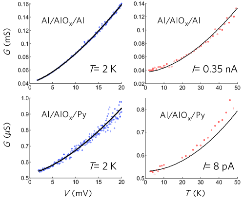
Figure S2 characterizes the conductance of the tunnel junctions, , for the representative 3-step NIN and FIN devices at small bias windows. The left panels show their voltage dependence at while the right panels show their temperature dependence at . In these regimes we can apply Glazman-Matveev theory for ordinary hopping via impurity chains [S1,S2]. We fit the obtained data by and , where with being the average impurity number in the chains under these small bias windows. From the voltage-dependent measurements, we obtain for the NIN sample and for the FIN sample. From the temperature-dependent ones, we obtain for the NIN sample and for the FIN sample. Therefore, the results obtained from the voltage- and temperature-dependent measurements are consistent, and show that at these small bias windows the transport in our 3-step tunnel barriers is dominated by conduction through two-impurity chains, meaning , where is the number of steps of the tunnel barrier. Note that in such small bias window condition, we can observe a perceivable background of and independent conductance due to direct and resonant tunneling, which becomes negligible in the usual working condition (e.g. 1 A constant current in Fig. 1(c) and 1(d) of the main text). The average impurity number slowly increases as the bias window increases [S2], as under the condition used in Fig. 1(e) of the main text where the number of impurity is closer to the number of deposition steps, . Finally, we point out that the above theoretical results [S1] are applicable only when max, where is the maximum acoustic phonon energy. We obtain that is on the order of 17 meV from Fig. 1(e) and 1(f) of the main text. Note that in Fig. 1(e) we have , and in this case the only important temperature dependence comes from that of the phonon population. It is also worth mentioning that the existence of impurities in the tunnel barrier can be also manifested as resonant peaks in the second derivative of the I(V) curve [S3]. Tinkey et al. have recently performed inelastic electron tunneling spectroscopy measurements (IETS) in SiO2 tunnel barriers and observe some sharp peaks not corresponding to Si or SiO2 vibrational modes in the IETS spectra. They observe that the peaks disappear as the barrier thickness is increased, which results in an increase of the barrier resistance. This happens due to the increase in the density of impurities when increasing the barrier thickness, resulting in a dense energetic distribution of impurities and disappearance of the peaks. After doing the corresponding calculations and comparison of our tunnel barrier resistance-area products with those in Ref. [S3], we conclude that the impurity-density in our tunnel barriers is too high for such peaks to be observed in the IETS.
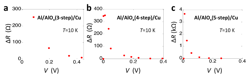
Figure S3 shows of several Al/AlO/Cu samples, with comparable voltage dependences to those shown in Fig. 2 of the main text. At large voltage values, follows the same voltage dependence as the total tunnel resistance, as explained by Eq. (2) of the main text. However, when the bias window reduces significantly, the small portion of impurity chains that are subject to magnetic field modulation (i.e., chains with an A-B sequence) becomes basically non-available compared to the total impurity chains, as well as to the direct and resonant tunneling channels. As a result, there are sharp drops of as the voltage is close to zero. It is worth pointing out that the voltage value where is maximum, , decreases as increases, with =85 mV, 12 mV and 5 mV for 3, 4 and 5, respectively. This can be qualitatively explained as follows: the higher the is, the longer the impurity chains are, and the more probable is to find A-B chains fulfilling , obtaining MR at smaller bias values.
Theory and numerical calculations
We describe the tunneling through two-impurity chains by generalizing the Anderson impurity Hamiltonian model to our tunneling case [S1],
| (S1) | |||||
denotes spin and are for Left/Right leads or impurities. () denotes impurity (lead) electrons and denotes phonons. The respective energy levels and occupation operators are , , and . is the on-site Coulomb repulsion energy. The Zeeman splitting energy at the -th impurity is , where is the sum of internal and external magnetic fields. and define the plane and is the angle between and the axis. and give rise to coupling between two impurities and with their nearby leads, and is the electron-phonon interaction matrix element. We have kept only linear inelastic tunneling terms which dominate the resonant tunneling at our finite bias [S1].
Master equations and the full analytical expression
To find the steady-state current across the impurity chains from the above Hamiltonian, we invoke non-equilibrium Green function techniques and derive master equations in the slave-boson representation [S4,S5]. They describe the competition between the Zeeman terms, impurity-lead coupling () and inter-impurity coupling (). The latter two in the weak coupling regime are expressed by and , respectively, where . Below we derive the general master equations for the A-B tunneling chain, under arbitrary magnetic fields at the two impurity sites and phonon population . We focus on the dominant contribution for which (i.e. ).
The basis states can be understood as , where has four possible states. We define density operators by and . Without loss of generality, we set , , and choose .
| (S2a) | |||||
| (S2b) | |||||
| (S2c) | |||||
| (S2d) | |||||
| (S2e) | |||||
| (S2f) | |||||
| (S2g) | |||||
| (S2h) | |||||
| (S2i) | |||||
| (S2j) | |||||
| (S2k) | |||||
The equations are not all independent but supplemented by . Having solutions to all matrix elements at , and , we get
| (S3) |
where
Equation (S3) leads to the approximated form in Eq. (1) of the main text. The negative term in Eq. (1) is a consequence of physical invariance under the rotation of spin coordinate, and it also occurs in B-A, A-A and B-B chains whose currents are independent of magnetic field. It is reflected in the off-diagonal elements in the master Eqs. (S2).
Calculation of averaged current expressions via AB chains, as well as on BA, AA, and BB chains
In the following we show how to obtain the averaged current expression plotted in Fig. 3(c) starting from the full current expression via an AB chain shown in Eq. (S2). To do that, we need to integrate over the internal field distributions at the two impurities, taking into account that they experience local internal magnetic fields due to spin interactions in addition to the external field. In order to do the integration, we express , and in Eq. (S2) in terms of the left and right internal fields and , and external field . If direction is set along , from one can obtain
| (S4) |
where . The angle between and can be expressed as follows
| (S5) |
As previously mentioned, the averaged current is a result of integration over internal field distribution probability ,
| (S6) |
where and, for simplicity, we assume that and are independent. For example, we may assume they are Gaussian distributions with finite variation around a mean value on the radial direction. Figure 3(c) is obtained in this way by a straightforward numerical integration of Eq. (S6). We assume because at this condition the impurity-assisted inelastic tunneling current is maximum [S1,S2].
For the purpose of gaining more insight of the magnitude of the signal and its trend with external magnetic field, we can make justified simplifications in order to carry out analytical integration. Since we are interested mainly in the regime of average internal field and its variation much larger than the tunneling rate, , we can properly use the approximation in Eq. (1) of the main text. Doing so, for any with spherical symmetry, at we have
| (S7) | |||||
where
| (S8) |
We have well matching the numerical result in Fig. 3(c), with the corresponding parameters used and .
In order to obtain an approximate but analytical trend of the current as a function of external field , we can further approximate by using , obtaining
| (S9) | |||||
where in the last step we have used the condition that the mean magnetic field of the distribution is much larger than its standard deviation, and replaced by in the integrand (this excellent approximation has been checked numerically for the whole range of ).
Last, we show explicitly that the current via other two-impurity chain types BA, AA and BB is magnetic field independent for the NIN devices. They are obtained by exactly solving similar master equations as those shown Eq. (S2).
| (S10) | |||||
| (S11) | |||||
| (S12) |
Discussion of new experimental results from other Groups
The mechanism proposed in the main text can readily explain the recurring magnetic field modulated signals from most 3T-FIN experiments when N is a semiconductor. The commonly seen feature that the MR signals depend less on the lead materials but more on the barriers is consistent with our framework. Here we manifest the versatility of this theory by explaining in detail some new observations that cannot be explained by previous theories [S6].
First, the Fe/MgO/Si devices in Ref. [S6] show coexistence of two effects: the total tunnel resistance saturates when the oxide barrier becomes ultrathin, whereas the MR signal shows a robust exponential dependence on the thickness of the oxide barrier. This phenomena can be straightforwardly explained by our tunneling theory of a FIN junction via one impurity, which is most likely to reside at the impurity-prone atomic interface between the oxide (MgO) and the Schottky barrier in the Si region. The total tunnel resistance saturation is a typical behavior of resonant tunneling via a single impurity. When the thickness of the MgO barrier is significantly reduced (), the resonant resistance is dominated by the smaller tunneling rate yielding
| (S13) |
Therefore, the tunneling resistance becomes constant, since is determined by the Schottky barrier which remains the same regardless of the MgO thickness.
Concerning the magnitude of the MR current , we can see that when it depends on the relative difference of the spin-dependent resonant tunneling rates, , in addition to . and are the spin-average tunneling rate and the spin polarization of the ferromagnet, and the dependence stems from the additional current-induced spin polarization of the impurity. Since ferromagnets are not pure half metal and is a fraction of 1, the intuitive current on/off picture induced by the magnetic field becomes effectively the difference of resonant tunneling rates from two opposite spins. When the tunnel barrier is really thin, their difference becomes extremely small because even the minority spin resonant tunneling rate between Fe and the impurity is much larger than that between Si and the impurity. As a result, the bottleneck of the ‘current-blocked state’ is caused by the Schottky barrier in the Si region rather than the minority spin tunneling from Fe. So the magnetic field modulation tends to be suppressed in this limit. More quantitative analysis is found in Ref. [S7].
All in all, we have
| (S14) |
Combining and with Eq. (2) of the main text, we have for . In the other limit of thick MgO barrier (), both and are proportional to . The magnetic modulation in this case is effective where is governed by the large relative difference . Again, we have . The two proportionality prefactors are of the same order of magnitude. Our MR picture leads to the overall exponential dependence of on the oxide thickness. This dependence has also been seen by other groups [S8]. The remaining control experimental results of Ref. [S7] are naturally understood within this MR picture. Replacing Si with metal eliminates the impurity-prone MgO/Si interface and Schottky barrier, therefore suppressing the impurity-assisted TMR. Inserting non-magnetic layer into the Fe/MgO interface turns off the spin polarization source [S8], and again suppresses our one-impurity-assisted TMR effect in FIN devices.
A noteworthy difference between FIN junctions where N is a semiconductor or a metal is the absence of the Schottky barrier in the latter ones. In both cases, treating the tunnel barrier by plasma oxidation is likely to eliminate the impurities inside the oxide layer. But defects can still be produced on the atomic interface between two different materials. When N is a semiconductor, the resonance current via impurities on the atomic interface between the oxide and the Schottky barrier can be large, and the MR signal comes from those impurities with large on-site Coulomb repulsion. When N is a metal, on the other hand, the tunnel current via impurities at the oxide/metal interface is negligible because the density of states in N is much higher than that of the impurities. This difference can then explain the negligible MR signal in our plasma-oxidized samples where both leads are metallic, and its appearance in experiments when N is a semiconductor.
[S1] L. I. Glazman and K. A. Matveev, Zh. Eksp. Teor. Fiz. 94, 332 (1988) [Sov. Phys. JETP 67, 1276 (1988)].
[S2] Y. Xu, D. Ephron, M. R. Beasley, Phys. Rev. B 52, 2843 (1995).
[S3] H. N. Tinkey, P. Li, I. Appelbaum, arXiv: 1405.2297 (2014).
[S4] Z. Zou and P. W. Anderson, Phys. Rev. B 37, 627(R) (1988).
[S5] J. C. Le Guillou and E. Ragoucy, Phys. Rev. B 52, 2403 (1995).
[S6] S. Sharma et al., Phys. Rev. B 89, 075301 (2014).
[S7] Y. Song and H. Dery, Phys. Rev. Lett. 113, 047205 (2014).
[S8] T. Uemura, K. Kondo, J. Fujisawa, K.-I. Matsuda, M. Yamamoto, Appl. Phys. Lett. 101, 132411 (2012).