Quantum size effect on the paramagnetic critical field in Pb nanofilms
Abstract
The quantum size effect on the in-plane paramagnetic critical field in Pb nanofilms is investigated with the use of the spin-generalized Bogolubov-de Gennes equations. It is shown that the critical field oscillates as a function of the nanofilm thickness with the period of ML (even-odd oscillations) modulated by the beating effect. This phenomena is studied in terms of the quantization of the electron energy spectra caused by the confinement of the electron motion in the direction perpendicular to the sample. The calculated values of critical fields for different nanofilm thicknesses are analyzed in the context of Clogston-Chandrasekhar limit. The influence of the thermal effect on the magnetic field induced superconductor to normal metal transition is also discussed. Furthermore, the thickness-dependence of the electron-phonon coupling and its influence on the value of the critical magnetic field are studied.
pacs:
74.78.-wI Introduction
The interplay between superconductivity and quantum confinement has attracted growing interest due to the unique phenomena which appear if the electron motion is limited to the size smaller than the coherence length.Zgirski et al. (2005); Tian et al. (2005); Janković et al. (2006); Altomare et al. (2006); Bezryadin et al. (2000); Savolainen et al. (2004); Shanenko et al. (2006) The huge progress in nanotechnology which has been made in the last decade allows to prepare uniform ultrathin films Pfenningstorf et al. (2002); Zhang et al. (2010); Uchihashi et al. (2011); Qin et al. (2009); Zhang et al. (2010); Uchihashi et al. (2011) with new superconducting properties which were predicted many years ago.Blatt and Thompson (1963) The oscillations of the superconducting energy gap as a function of the nanofilm thickness were predicted by Blatt and ThompsonBlatt and Thompson (1963) in 1963. The authors of Ref. Blatt and Thompson, 1963 showed that the quantum-well states which are created due to the confinement of the electron motion in the direction perpendicular to the film, greatly modulate the electron density of states near the Fermi level and thus significantly affect the superconducting energy gap of the nanofilm. As a result, one would expect a significant increase of the energy gap each time the bottom of a subband passes through the Fermi sphere. Nevertheless, either the experimental studies carried out in these years did not exhibit such an effect or the observed oscillations differed quantitatively from the theoretical predictions.Orr et al. (1984) This inconsistency was attributed to the technological difficulties in the preparation of uniform films which were typically polycrystalline and contained a large number of defects. Since then, many technological obstacles were overcame what reopened the issue for the quantum confinement effect on the superconductivity in the nanoscale regime.
Recently, Guo at al.Guo et al. (2004) have fabricated ultrathin Pb films on Si(111) substrate and observed the oscillations of the critical temperature as a function of the number of atomic monolayers. The origin of oscillations associated with the quantum confinement has been confirmed independently by the measurements of the quantum-well energies by using photoemission spectroscopy. The results presented in Ref. Guo et al., 2004 have concerned only films with the thickness greater than ML because of problems with stability of the even-layered films below ML. The study of Pb nanofilms has been extended by Eom et al.Eom et al. (2006) who have reported oscillations in the epitaxially grown crystalline Pb films in the thickness range ML. In Ref. Eom et al., 2006 the critical temperature has been measured using scanning tunneling micoroscopy which allows to avoid ambiguities associated with the Au layer which has to be applied in the transport measurements reported in Ref. Guo et al., 2004. It has been found that there is a direct correlation between the oscillations of the density of states at the Fermi level and oscillations. Also, the measurements of the critical temperature for Pb nanofilms on Si(111) substrate have revealed one more interesting phenomena called bilayer or even-odd oscillations. As it has shown, the critical temperature for nanofilms with even number of monolayers is greater than the one for nanofilms with odd number of monolayers in proper ranges of nanofilm thickness. This dependence reverses (odd monolayer films have the critical temperature greater than even monalayer films) with the periodicity of ML depending on the experiment.Guo et al. (2004); Eom et al. (2006) This effect has been theoretically investigated by Shanenko et al. in Ref. Shanenko et al., 2007 and observed in many experiments.Özer et al. (2006, 2007); Zhang et al. (2010)
The new direction of studies devoted to superconductivity in nanoscale regime concerns the effect of quantum confinement on the superconductor to normal metal transition induced by the magnetic field. It has been theoretically shown, that a cascade of jumps in the energy gap as a function of the magnetic field occurs in the metallic nanowires.Shanenko et al. (2008) This effect has been explained in terms of depairing in the subsequent bands when the magnetic field increases. Shanenko et al. (2008) The oscillations of the perpendicular upper critical field in ultrathin lead films have been reported by Bao et al. in Ref. Bao et al., 2005. This experimental report has shown the even-odd oscillations of the upper critical field for Pb nanofilms. It is also worth mentioning that very recently an interesting effect has been found in amorphous Pb nanofilm. Gardner et al. (2011) Namely, the increase of the critical temperature has been observed after application of a parallel magnetic field to the sample.
According to our knowledge, the theoretical study of the superconducting-normal metal transition induced by the in-plane magnetic field and its interplay with the quantum confinement has not been reported until now. In the present paper we investigate the superconductor-normal metal transition driven by the in-plane magnetic field for Pb nanofilms. We show that the critical field oscillates as a function of the nanofilm thickness with the period of ML (even-odd oscillations) modulated by the beating effect with the periodicity of ML. The calculated paramagnetic critical field differs from the Clogston-Chandrasekhar paramagnetic bulk limit.Clogstone (1962); Chandrasekhar (1962) We also discuss the thermal effect and determine formulas for in the limit . Finally, we take into account the oscillatory behavior of the electron-phonon coupling occurring in nanofilms and calculate as a function of the nanofilm thickness for the experimental samples for which a good agreement of theory and experiment has been found in the study of the critical temperature. Chen et al. (2012)
II Theoretical method
The superconducting properties of the conventional phonon-mediated pairing system for the high quality single crystalline structures can be described with the use of the BCS theory, which leads to the Bogoliubov-de Gennes (BdG) equations in the form
| (1) |
where and are the spin-dependent electron-like and hole-like wave functions (), is the superconducting energy gap and is the quasi-particle energy. In the presence of the in-plane magnetic field the Hamiltonian is given by
| (2) |
where corresponds to the spin and is related to the spin ,
is the free electron mass, is the Bohr magneton, is the chemical potential and
is the vector potential related to the parallel magnetic field.
In the present paper we neglect the orbital effects and consider the superconducting nanofilms in
the clean paramagnetic limit. This approximation is justified for the
nanofilms with the thickness less than the magnetic length .
The use of the Clogston-Chandrasekhar paramagnetic field for Pb T gives nm
which means that the paramagnetic approximation can be used for Pb nanofilms with thickness
less than ML (we assume the lattice constant for Pb, nm).
In the paramagnetic limit the Hamiltonian can be further simplified to the form
| (3) |
If we assume the periodic boundary conditions in the plane, the quasi-particle wave functions can be expressed as
| (4) |
where denotes the opposite spin. In the equation (4) the index has been replaced by , where , are the free electron wave vector components in the and direction, while labels the quantum states in the direction. By substituting the wave function given by (4) into the BdG equations (1) we obtain two independent set of equations
| (5) |
and
| (6) |
where
| (7) |
and . Assuming that the system is infinite in the and directions (), the order parameter can be expressed as
| (8) | |||||
where is the electron-phonon coupling and is the Fermi-Dirac distribution. The summation in Eq. (8) is carried out only over these states for which the single-electron energy satisfies the condition , where is the Debye frequency and is given by
| (9) | |||||
where is the nanofilm thickness in the -direction. The system of equations (5)-(6) and equation (8) are solved in a self consistent manner until the convergence is reached. As a result the spatially varying energy gap is obtained. In the further analysis we often use spatially averaged energy gap defined as
| (10) |
Since the chemical potential for nanostructures strongly deviates from the bulk value, for each nanofilm thickness we determine the chemical potential by using the formula
| (11) | |||||
In the calculations we adopt the the hard-wall potential profile as the boundary conditions in the direction.
The set of self-consistent equations can lead to solutions with even for the values of the magnetic field
for which the superconducting phase is already not stable - its free energy is greater than the free energy corresponding
to the normal metal solution (). That is why in determining the critical field one should calculate and compare
the free energy of the normal and superconducting phase, as it is done here.
III Results
In this section we analyze the superconductor to normal metal transition induced by the parallel magnetic field. The thickness range under consideration is chosen based on the experiments which present measurements for the Pb nanofilms with thickness varying from 5 to 30 ML. The calculations have been carried out for the following values of the parameters: where is the bulk density of the single-electron states at the Fermi level, meV, the lattice constant nm and the bulk critical temperature K which corresponds to the energy gap meV. Within the parabolic band approximation used in the present model, the Fermi level in the bulk is treated as a fitting parameter. Shanenko et al. (2007) Its value is determined based on the experimental results from the photoemission spectroscopy.Eom et al. (2006); Zhang et al. (2005) We take on eV which corresponds to the nm being about four times the single monolayer thickness .
III.1 Paramagnetic critical field oscillations
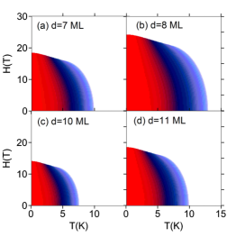
In Fig. 1 the in-plane critical field as a function of the nanofilm thickness is presented for different temperatures . The value of is determined based on calculations of the energy gap as a function of the magnetic field and is defined as the field for which the spatially averaged energy gap drops below .
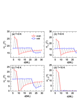
Fig. 1(a) displays the oscillatory behavior of the paramagnetic critical field with the period of ML. In the thickness range ML the critical field for the even-layered films is higher than the critical field for the odd-layered films. This relation reverses for films with the number of monolayers varying from 10 to 22 ML and changes again in the range ML. The periodicity of such modulation is equal to ML. The even-odd (bilayer) oscillations with the beating effect have been observed in recent measurements of the critical temperature Eom et al. (2006); Guo et al. (2004) and the electron-phonon coupling in Pb thin nanofilms. Zhang et al. (2010) In these experiments the modulation periodicity varies from 7 ML in Ref. Eom et al., 2006 to 9 ML in Ref. Zhang et al., 2005 indicating that this quantity depends on the quality of the nanofilm and might vary from one experiment to another. Both the oscillations of in Fig. 1 result from the confinement of the electron motion in the direction perpendicular to the film. In the ultra thin nanofilms, the confinement of the electron motion leads to the quantization of its energy. The Fermi sphere transforms into the series of parabolic subbands, positions of which on the energy scale decreases with increasing nanofilm thickness. Since the Cooper-pairing in the phonon-mediated superconductor is determined by the number of the electron states in the energy window ( is Debye energy), the superconducting energy gap increases each time, the subsequent subband passes through the Fermi surface. The presented mechanism, predicted theoretically in 1963 by Blatt and Thomson Blatt and Thompson (1963), results in the tooth-like oscillations of the spatially averaged energy gap as a function of the nanofilm thickness. The tooth-shape of the energy gap oscillations is directly related to the changes of the electron density of states in the vicinity of the Fermi level. It abruptly increases when the subband minima reach the Fermi level and then exponentially decreases with increasing nanofilm thickness. Blatt and Thompson (1963) The zero temperature energy gap as a function of the number of monolayers for Pb nanofilms is presented in Fig. 2.
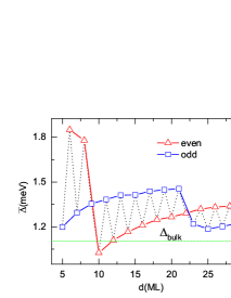
We see that the shape of oscillations at K [Fig. 1(a)] is directly related to the shape of oscillations in Fig. 2. It is because, in the ultra thin nanofilms with in-plane magnetic field, the pair-breaking mechanism is mainly governed by the paramagnetic (Pauli) limit which is given by Clogston-Chandrasekhar Clogstone (1962); Chandrasekhar (1962) (CC) formula, . Therefore, the bilayer oscillations of the in-plane critical field result from the contribution of the subsequent subbands to the superconducting energy gap.

In Fig. 3 the quasi-particle energy versus the wave vector is presented for the film thickness ML (a,b) and ML (c,d). The first pair of thicknesses correspond to the range in which is higher for the even-layered films while the second pair is related to the range for which a reversed situation is observed. We see that for the film thickness ML three lowest subbands participate in the creation of the superconducting state [Fig. 3(a)]. Increasing the thickness by one monolayer causes that the forth subband begins to contribute to the superconducting phase which leads to the enhancement of the energy gap and the critical field depicted in Fig. 1(a). In the thickness range ML the subsequent subbands pass through the Fermi level only if the number of monolayers is even. The period of the passages can be well estimated by the single-electron energy level in the form , where the hard-wall potential is assumed in the direction. It allows us to determine the period , which for the assumed effective Fermi level gives ML. The difference between 2 ML and the real period of the quantum well states which pass through the Fermi surface ( ML) results in the beating effect observed in Fig. 1(a). In Fig. 3(c,d) the new subband () appears for the odd-layered film ( ML) which is in contradiction to the pair ML [see Fig. 3(a)(b)] for which the subsequent subband () appears for the even-layered film ( ML). The interval in which the critical field for the odd-layered films is higher than for the even-layered films ranges from ML to ML. The source of the beating effect is clearly visible in Fig. 4 in which the energy of the quantum well states as a function of the nanofilm thickness is presented.
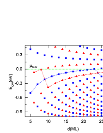
In Fig. 4 only the states with the energy below Fermi level (set as zero energy) are occupied and contribute to the Coooper pair condensation. The closer to the Fermi energy they are located the larger is their contribution to the density of states. In Fig. 4 the energies closest to the Fermi level are joined by the blue (red) line for the even (odd) number of monolayers. Note that such procedure leads to the “structure”, in the sense of the shape, exactly the same as depicted in Fig. 1(a).
Let us now discuss the value of the paramagnetic critical field obtained from our calculations. It is well-known that in the ultra thin films with the in-plane magnetic field, the orbital-magnetic interaction is strongly reduced and the upper limit for the critical field is determined by the paramagnetic breakdown of the Cooper pairs. The formula for the paramagnetic critical field in the bulk was derived by Clogston and Chandrasekhar Clogstone (1962); Chandrasekhar (1962) and has the form which for Pb gives T. This value strongly differs from the critical field obtained in our calculations which vary from T to T. Such deviation for the Pb nanofilms has been recently reported in Ref. Sekihara et al., 2013 in which the experimental critical field , has been much higher than the paramagnetic limit . It seems that such discrepancy results from the fact that due to the electron confinement in the nanofilm, the energy gap is enhanced (Fig. 2) which leads to increase of the . Nevertheless, the use of the CC formula with the spatially averaged energy gap calculated for each nanofilm thickness still produces the value of the critical field which is lower than the results from numerical solution of the spin-generalized BdG equations, i.e. for ML, T while calculated T. This fact can be understood if we realize that the superconducting energy gap depends on the coordinate and is not uniform as in the expression for Clogston-Chandrasekhar field. Taking into account the correction which results from the averaging of the energy gap over the coordinate we introduce the thickness-dependent parameter and express the critical field in the form
| (12) |
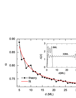
Fig. 5 shows that the parameter is the decreasing function of the thickness and for sufficiently large thickness reaches the value . The asymptotic behavior of for results from the fact that for the large thickness the spatially varying energy gap diverges to the uniform one - compare for the thicknesses and ML presented in the inset of Fig. 5. The dependence can be well fitted using the formula (the thickness denotes the number of monolayers - see Fig. 5) which clearly indicates that the parameter diverges to the bulk value in accordance to the CC theory. It should be noted that the smallest difference between the quasiparticle energy in the superconducting state and the Fermi energy is the same for each band created due to the confinement of electrons in the direction perpendicular to the sample (c.f. Fig. 3). Using this energy gap, instead of the averaged energy gap in the CC formula, one obtains the same values of critical fields as the ones resulting from the BdG equations.
III.2 Thermal effect
In the present subsection we discuss in detail the effect of temperature on the superconductor to normal metal transition induced by the in-plane magnetic field. The critical field presented in Fig. 1 for different temperatures shows that its value gradually decreases with increasing temperature. Since the critical temperature oscillates as a function of the nanofilm thickness (similarly to the energy gap depicted in Fig. 2), at the temperature K, the nanofilms with the thickness ML are superconducting while the film with the thickness therebetween transits to metallic state.
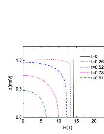
In Fig. 6 we present the spatially averaged energy gap as a function of the magnetic field and temperature. The results in Fig. 6 have been calculated for the nanofilm thicknesses and ML. To make it more transparent, the value of the energy gap in each of the figures is normalized with respect to its maximum.
In Fig. 6 we can see that the range of the magnetic field and temperature for which the sample is superconducting is larger for the thickness for which the enhancement of the energy gap (see Fig. 2) is found. Nevertheless the thickness-dependence is not visible in the normalized critical magnetic field as a function of , where and is the critical field at and the critical temperature for , respectively. In other words the phase diagram presented in Fig. 7 looks the same for each film thickness which is understandable if we recall our restriction to the Pauli limit with no orbital effect.
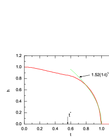
The initial behavior of at the temperature close to () can be well estimated by the formula . Note that, in contrast to the orbital limit with no Pauli effect, the slope of at critical temperature is infinite and in the vicinity of is expressed by . In this range the transition at is of second order. In the Pauli limit the second order transition is suppressed with decreasing temperature and below it becomes the first order. Maki (1964, 1966) The first to second order transition is clearly presented in Fig. 8 in which the energy gap versus magnetic field is presented for different temperatures.
Note that the critical field at is not equal to the paramagnetic limit but is further enhanced. A detailed discussion of the deviation of the critical field from is presented in sec. III.A.
III.3 Thickness dependent electron-phonon coupling
The microscopic model based on the spin-generalized BdG equations allows to analyze superconductor to normal metal transition in the nanofilms when its thickness is reduced to few nanometers. However, in the nanoscale regime, the confinement affects not only the electronic spectrum, but also the phononic degrees of freedom. The phonon dispersion in thin films strongly deviates from that in the bulk. Nabity and Wybourne (1992) The quantization of the phononic spectra in the nanofilms and its influence on and energy gap oscillations have been considered in Ref. Hwang et al., 2000. However, the effect of the confinement on the electron-phonon coupling strength has not been included. This lack has been recently supplemented by Saniz et al. in Ref. Saniz et al., 2013. In this paper Saniz et al. (2013) the authors have investigated the effect of confinement on the strength of the electron-phonon coupling as well as the electronic spectrum and its influence on the oscillations of the critical temperature. The formula for the phonon-mediated attractive electron-electron interaction has been derived with the use of the Green function approach beyond the contact potential approximation. It has been found that the increase of the critical temperature observed in superconducting nanofilms is due to the increase of the number of phonon modes what results in the enhancement of the electron-phonon coupling. In contradiction to previous models Shanenko et al. (2006, 2007), this study predicts the suppression of the critical temperature with increasing density of states at the Fermi level. Such conclusion seems not to be confirmed by recent experiments in which the direct correlation between the oscillations and the energy distribution of the quantum well states in nanofilms is observed. Eom et al. (2006)


In order to determine the realistic value of the electron-phonon coupling which occurs in experiments, there is one more aspect which should be taken into consideration. Note that the results presented in this paper regard the so-called freestanding nanofilms. In fact, Pb films are grown on Si(111) substrate and, for the purpose of the transport measurements, are covered by the layer of Au. Both these layers strongly affect the electron-phonon coupling in the nanofilm due to the interface effect. It has been recently observed Zhang et al. (2005) that the electron-phonon coupling for Pb nanofilms on Si substrate is lower than in the bulk and diverges to the bulk value with increasing film thickness. The results presented in Ref. Zhang et al., 2005 indicate that the interface effect has a strong impact on the electron-phonon coupling and should be taken into account in the presented model in order to reproduce the experimental data. The simple approximation which allows to take this effect into account has been recently proposed by Chen et al. in Ref. Chen et al., 2012. It has been assumed Chen et al. (2012) that in the first approximation the spatially-dependent electron-phonon coupling can be well estimated by the formula
| (13) |
where is the interface thickness with the electron-phonon coupling and is the electron-phonon coupling in the bulk. Averaging over the coordinate and including the oscillatory behavior of coefficient reported in experiments Zhang et al. (2005) leads to the formula (for details see Ref. Chen et al., 2012)
| (14) |
where is a periodic function, is the number of monolayers, is the Fermi wavelength and is the lattice constant. Since the period of oscillations in Pb nanofilms is measured to be ML, the authors of Ref. Chen et al., 2012 have reduced the function to only two parameters: for an odd number of monolayers and for an even number of monolayers. By appropriate choice of these parameters and by setting the Fermi level to the value corresponding to the period of the quantum-size oscillations ( ML) one can well reproduce the experimental data of coming form Ref. Özer et al., 2006; Eom et al., 2006; C et al., 2009. The values of the parameters used for each of the mentioned references is presented in table 1.
| Reference | |||
|---|---|---|---|
| Ref.Eom et al.,2006 | 0.36 | ||
| Ref.Özer et al.,2006 | 0.39 | ||
| Ref.C et al.,2009 | 0.39 |
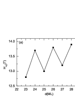
In the present subsection we use these parameters to predict the zero temperature in-plane critical field as a function of the nanofilm thickness. We believe that such procedure allows to determine the realistic value of the critical field comparable with recent experimental measurements. Sekihara et al. (2013) The thickness-dependent oscillations of the zero temperature critical field are presented in Fig. 9. Although the periodicity of the oscillations for each of the considered references is the same and equal 2 ML, the characteristics of these oscillations are different and vary form one experiment to another. This difference regards the overall trend of which is an increasing function of the thickness in case of Refs. C et al., 2009; Özer et al., 2006 but decreasing in the case of Ref. Eom et al., 2006. Note that the values of the critical field in Fig. 9 are suppressed as compared to the critical field calculated with the electron-phonon coupling for the bulk [compare with Fig. 1(a)].
IV Summary
The superconductor to normal metal phase transition driven by the magnetic field for Pb nanofilms is investigated with the use of the BdG equations. Only the Pauli pair-breaking mechanism is included as it is assumed that the external magnetic field is parallel to the surface of the nanofilm. It is shown that the even-odd oscillations of the critical magnetic field appear as the thickness of the sample is increased. The shape of the oscillations is directly related to the shape of the thickness dependence of the superconducting gap. The beating effect visible in the oscillations is discussed in the context of the energy of the quantum well states which appears due to the confinement of the electron motion in the direction perpendicular to the sample. As it has been shown the period in the nanofilm thickness between two neighbouring peaks in the critical field is equal to 2.14 ML. As the number of the monolayers has to be an integer the beating effect appears in the oscillatory behavior of and . We also show that the zero-temperature critical field in the nanofilms is higher than the Clogston - Chandrasekhar paramagnetic limit and it diverges to the CC value for sufficiently thick films. This fact is explained in term of the spatially varying energy gap induced by the confinement. The phase diagrams in the plane are presented for different values of . According to the obtained results the thickness-dependence is not visible in the phase diagrams when both the field and the temperature are normalized and . Moreover, the interface effect on the electron-phonon coupling is included by using a simple approximation proposed in Ref. Chen et al., 2012. This leads to a spatially dependent factor and its oscillatory behavior with increasing nanofilm thickness. As it is shown this effect leads to a suppression of the critical field values in comparison to the ones corresponding to the bulk. We believe that such approach allows for comparison of the calculated oscillations with the experimental results.
V Acknowledgments
Discussions with Józef Spałek are gratefully acknowledged. This work was financed from the budget for Polish Science in the years 2013-2014. Project number: IP2012 048572. M. Z. acknowledges the financial support from the Foundation for Polish Science (FNP) within project TEAM.
References
- Zgirski et al. (2005) M. Zgirski, K. P. Riikonen, V. Touboltsev, and K. Arutyunov, Nano Lett. 5, 1029 (2005).
- Tian et al. (2005) M. L. Tian, J. G. Wang, J. S. Kurtz, Y. Liu, M. H. W. Chan, T. S. Mayer, and T. E. Mallouk, Phys. Rev. B 71, 104521 (2005).
- Janković et al. (2006) L. Janković, D. Gournis, P. N. Trikalitis, I. Arfaoui, T. Cren, P. Rudolf, M. H. Sage, T. T. M. Palstra, B. Kooi, J. De Hosson, A. Karakassides, K. Dimos, A. Moukarika, and T. Bakas, Nano Lett. 6, 1131 (2006).
- Altomare et al. (2006) F. Altomare, A. M. Chang, M. R. Melloch, Y. Hong, and C. W. Tu, Phys. Rev. Lett. 97, 017001 (2006).
- Bezryadin et al. (2000) A. Bezryadin, C. N. Lau, and M. Tinkham, Nature 404, 971 (2000).
- Savolainen et al. (2004) M. Savolainen, V. Toulboltsev, P. Koppinen, K. P. Riikonen, and K. Arutyunov, Appl. Phys. A: Mater. Sci. Process. 79, 1769 (2004).
- Shanenko et al. (2006) A. A. Shanenko, M. D. Croitoru, M. Zgirski, F. M. Peeters, and K. Arutyunov, Phys. Rev. B 74, 052502 (2006).
- Pfenningstorf et al. (2002) O. Pfenningstorf, A. Petkova, H. L. Guenter, and M. Henzler, Phys. Rev. B 65, 045412 (2002).
- Zhang et al. (2010) T. Zhang, P. Cheng, W. J. Li, Y. J. Sun, X. G. Wang G, Zhu, K. He, L. L. Wang, X. C. Ma, X. Chen, Y. Y. Wang, Y. Liu, L. H. Q, J. F. Jia, and Q. K. Xue, Nat. Phys. 6, 104 (2010).
- Uchihashi et al. (2011) T. Uchihashi, P. Mishra, M. Aono, and T. Nakayama, Phys. Rev. Lett. 107, 207001 (2011).
- Qin et al. (2009) S. Qin, J. Kim, Q. Niu, and C. K. Shih, Science 324, 1314 (2009).
- Blatt and Thompson (1963) J. M. Blatt and C. J. Thompson, Phys. Rev. Lett. 10, 332 (1963).
- Orr et al. (1984) B. G. Orr, H. M. Jaeger, and A. M. Goldman, Phys. Rev. Lett. 53, 2046 (1984).
- Guo et al. (2004) Y. Guo, Y. F. Zhang, X. Y. Bao, T. Z. Han, Z. Tang, L. X. Zhang, W. G. Zhu, E. G. Wang, Q. Niu, Z. Q. Qiu, J. F. Jia, Z. X. Zhao, and Q. K. Xue, Science 306, 1915 (2004).
- Eom et al. (2006) D. Eom, S. Qin, M. Y. Chou, and C. K. Shih, Phys. Rev. Lett. 96, 027005 (2006).
- Shanenko et al. (2007) A. A. Shanenko, M. D. Croitoru, and F. M. Peeters, Phys. Rev. B 75, 014519 (2007).
- Özer et al. (2006) M. M. Özer, J. R. Thompson, and H. H. Weitering, Nat. Phys. 2, 173 (2006).
- Özer et al. (2007) M. M. Özer, Y. Jia, Z. Zhang, J. R. Thompson, and H. H. Weitering, Science 316, 1594 (2007).
- Shanenko et al. (2008) A. A. Shanenko, M. D. Croitoru, and F. M. Peeters, Phys. Rev. B 78, 024505 (2008).
- Bao et al. (2005) X. Y. Bao, Y. F. Zhang, Y. Wang, J. F. Jia, Q. K. Xue, X. C. Xie, and Z. X. Zhao, Phys. Rev. Lett. 95, 247005 (2005).
- Gardner et al. (2011) H. J. Gardner, A. Kumar, L. Yu, P. Xiong, M. P. Warusawithana, L. Wang, O. Vafek, and D. G. Schlom, Nat. Phys. 7, 895 (2011).
- Clogstone (1962) A. M. Clogstone, Phys. Rev. Lett. 9, 266 (1962).
- Chandrasekhar (1962) B. S. Chandrasekhar, Appl. Phys. Lett. 1, 7 (1962).
- Chen et al. (2012) Y. Chen, A. A. Shanenko, and F. M. Peeters, Phys. Rev. B 85, 224517 (2012).
- Zhang et al. (2005) T. Zhang, , J. F. Jia, Z. Tang, S. Q. T, Y. Guo, Z. Q. Qiu, and Q. K. Xue, Phys. Rev. Lett. 95, 096802 (2005).
- Sekihara et al. (2013) T. Sekihara, R. Masutomi, and T. Okamato, Phys. Rev. Lett. 111, 057005 (2013).
- Maki (1964) K. Maki, Prog. Theor. Phys. 31, 945 (1964).
- Maki (1966) K. Maki, Physical Review 148, 362 (1966).
- Nabity and Wybourne (1992) J. C. Nabity and M. N. Wybourne, Phys. Rev. B 44, 8990 (1992).
- Hwang et al. (2000) E. H. Hwang, S. Das Sarma, and M. A. Stroscio, Phys. Rev. B 61, 8659 (2000).
- Saniz et al. (2013) R. Saniz, B. Partoens, and F. M. Peeters, Phys. Rev. B 87, 064510 (2013).
- C et al. (2009) B. C, P. Hong, F. Patthey, I. Y. Sklyadneva, R. Heid, P. M. Echenique, K. P. Bohen, E. V. Chulkov, and W. D. Schneider, Phys. Rev. Lett. 102, 207002 (2009).