Graphene based sensors: theoretical study
Abstract
Graphene, a 2-dimensional monolayer form of sp2 hybridizated carbon atoms, is attracting increasing attention due to its unique and superior physicochemical properties. Covalently functionalized graphene layers, with their modifiable chemical functionality and usefull electrical properties, are excellent candidates for broad range of sensors, suitable for biomedical, optoelectronic and environmental applications. Here, we present extensive study of transport properties of sensors based on covalently functionalized graphene monolayer (GML) with graphene electrodes. The transmissions, density of states and current-voltage characterisctics supported by analysis of charge distribution of GML functionalized by -CH3, -CH2, -NH2, -NH and -OH-CH3, -CH2, -NH2, -NH and -OHGreen’s function (NEGF). Further, we demonstrate how to control the device sensitivity by manipulating: (i) concentration, (ii) particular arrangement, and (iii) type of surface groups. We explain the underlying detection physical mechanisms. Comparisons of the theoretical results to available experimental data are provided and show good agreement.
I Introduction
Nowadays graphene, a 2-dimensional semimetalic monolayer, a form of sp2 hybridizated carbon, attracts a lot of research activity owing to its unique electronic, mechanical and thermal propertiesGeim and Novoselov (2007). Graphene layers (GLs) are emerging as the very promising candidates for a new generation of electronic devicesPark and Ruoff (2009); Pacile et al. (2011); Sengupta et al. (2011); Georgakilas et al. (2012). From electronic point of view, graphene has several properties such as extremely high mobility, high surface area-to-volume ratio, fast electron transfer rate, ballistic transport on submicrometer scale, the electron conductivity even higher than for copper at room temperature or good biocompabilityLuque et al. (2010); Neto et al. (2009); Sarma et al. (2011); Kuila et al. (2012); Pramanik and Kang (2011); Basu and Bhattacharyya (2012); Pramanik and Kang (2010), which can be beneficial in the design electrochemical sensors. However, pure graphene monolayer (GML) has zero energy band gap, which hinders direct application of graphene layer in digital electronics. The covalent functionalization of GLs is one of the possible solutionsMao et al. (2013) to this problem. It opens the band gap and facilitates the usage of graphene monolayers as sensors Georgakilas et al. (2012). It was already reported that graphene based sensors can detect even individual moleculesLiu, Liu, and Zhu (2011); Basu and Bhattacharyya (2012); Schedin et al. (2007). Because of biocompability of graphene, it is possible to detect glucoseWang et al. (2010); Liu et al. (2010), proteinsAng et al. (2008), DNALu et al. (2009) or even bacteriaMohanty and Berry (2008); Chang et al. (2013). Smaller, faster and more sensitive sensors (i.e., graphene based) are nowadays searched for environmental applicationsShao et al. (2010); Kehayias et al. (2013); Li, Cao, and Hu (2012).
Proper sensing depends on many parameters, which demand a trade off between mechanical and electrical properties such as interface accessibility with molecular sensitivity and selectivity at room temperature or mechanical and electrical robustness. At pristine graphene surface, therefore, the direct adhesion of the sensed substances to the graphene is rather unprobable. Functionalization with small molecules can resolve this problem enhancing chemisorption of target molecules to the basal plane of graphene. Moreover, it was shownErni et al. (2010) that adsorption of molecules, such as primary amines, methyl or hydroxyl groups, is highly probable when graphene membranes are unavoidably exposed to air and various organochemical solutions during preparation.
Unfortunately, functionalization, especially covalent one, can lead to many unwanted changes in morphology, both on local and global scale, elastic and electronic propertiesBoukhvalov and Katsnelson (2009, 2010); Milowska, Birowska, and Majewski (2011, 2012); Milowska and Majewski (2013), and also modify transport characteristics. To analyse this effect, we have performed studies of transport properties of GMLs functionalized with simple organic molecules such, as -NH2, -NH, -CH2, -CH3, and -OH, at low concentrations.
II Theoretical methods
The electronic coherent transport has been studied employing non-equilibrium Green’s function (NEGF) technique, within the Keldysh formalism, a rather standard procedure for treatment of transport in coherent regimeDatta (1995). The studied structures have been treated as two-probe systems with the central scattering region sandwiched between semi-infinite source (left) and drain (right) electrode regions (as shown in Fig. 1 (a)). The transmission coefficient of electrons (incident at energy E) through the central scattering region constituting the device (under the bias voltage Vb equal to the electrochemical potential difference between the left and right electrodes, eVb = ) T(E,Vb) has been calculated using the following expression:
| (1) |
where are matrices that take into account the coupling of the central region to the right(left) electrode, and is retarded Green’s function of the system. The conductance can be expressed as follows Datta (1995)
| (2) |
where is the unit of quantum conductance and is advanced Green’s function. The current flowing through the scattering region has been calculated according to Landauer-Buttiker formula, i.e., assuming the limit of small bias, which is justified for the range of the external voltages considered in the present study:
| (3) |
We have used TranSIESTA Brandbyge et al. (2002) package to calculate the transmission coefficients T(E, Vb) according to Eq. 1, and then current-voltage I(Vb) characteristics due to Eq. 3. The source (left) and drain (right) electrodes contain 16 carbon atoms each. The central region, with electrode extensions, contains in each case 80 carbon atoms to which functionalized groups are attached. For the geometry relaxations of central region without electrodes extensions (48 C atoms with adsorbates), we have used SIESTA package Ordejon, Artacho, and Soler (1996); Soler et al. (2002); Sanchez-Portal et al. (1997). The C atoms, adjacent electrode extensions were fixed to perfectly match with those regions meaning that functionalized structure is stressed (ca. 1.5 kbar).
The so-called PBE form of the generalized gradient approximation (GGA) Perdew, Burke, and Ernzerhof (1996) has been chosen for the exchange correlation density functional. Computations have been performed employing following parameters of the SIESTA package that determine numerical accuracy of the results: double--plus-polarization basis, kinetic cut-off for real-space integrals of 500 Ry, the self-consistency mixing rate of 0.1, the convergence criterion for the density matrix of 10-4, maximum force tolerance equal to 0.001 eV/Å, and 8x8x3 k-sampling in Monkhorst Pack scheme. For the transport calculations, the complex energy contour has been always set to value below the lowest energy in the energy spectrum of each system. The number of points along the arc part and on the line of the contour have been set to 16 and 10, respectively, whereas number of Fermi poles to 16. For the current calculations, we have used default value of small finite complex part of the real energy contour (10-6 Ry) and increased number of points on the close-to-real axis part of the contour in the voltage bias window to 10. For accuracy of transmission spectra, the energy window has been in the range of (-3,3) eV, the number of points for the computation of the transmission function has been quite high (500) and the number of eigenvalues of the transmission matrix has been set to 3. All calculation have been performed with spin polarization.
III Results and discussion
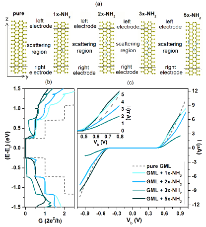
Motivated by experimental data Baraket et al. (2012), we have started our studies of transport properties of functionalized GMLs with primary amines. The schematic view of studied functionalized systems: pure graphene monolayer, graphene functionalized with one, two, three and five -NH2 group are shown in Fig. 1 (a).
| No. | Type | (eV) | (eV) |
|---|---|---|---|
| 1 | -NH2 | -0.314 | 1.215 |
| 2 | -NH2AA | -0.429 | 1.212 |
| 2 | -NH2AB | -0.442 | 1.155 |
| 3 | -NH2 | -0.537 | 1.192 |
| 5 | -NH2 | -0.412 | 1.303 |
| 2 | -CH3 | -0.779 | 1.132 |
| 2 | -OH | -1.498 | 1.069 |
| 2 | -NH | -1.509 | 1.064 |
| 2 | -CH2 | -1.893 | 1.283 |
Chemisorption of -NH2 groups leads to breaking one of -bonds and sp2 to sp3 rehybridization of C-C bonds. Unpaired electron, which forms this broken bond remains at the neighbouring C atom. The chemisorption of the next group on different sublattice is more energetically favourable than on the same sublattice (i.e. for -NH2 group the difference in Eads/N is equal to 0.033 eV per attachment, see Tab. 1). Similar observation concerning hydrogen functionalization of graphene was presented by Boukhvalov and Katsnelson in Ref.Boukhvalov and Katsnelson (2009). Therefore, it is more probable that in an experiment a reduction of conductance with growing density of amines will be observed rather than conservation of conductance at pristine graphene level.
Garcia-Lastra et al.Garcia-Lastra et al. (2008) showed that there is a systematic dependence of transmission on the position of the adsorbed molecules to the lateral surface of metallic nanotubes. The behaviour of the conductance as depicted in Fig. 1 (b) is characteristic for metallic carbon nanotubes with single adsorbed molecule placed on top of carbon atom, or more adsorbed molecules placed on equivalent lattice sites (say ) with certain positions determined by the vectors , with , where , , and are integers, and and are two primitive translations of the graphene lattice. This behaviour can be understood in terms of coinciding K, K’ and , the high symmetry points, in graphene systems where groups are adsorbed at sites , being multiple of 3 Garcia-Lastra (2010). In the case studied in this paper, the two -NH2 molecules were placed at graphene lattice sites with equal to and at so-called top positions, therefore, fulfilling the ruleGarcia-Lastra et al. (2008) and indicating that graphene layer can be treated as metallic carbon nanotube of infinite radius. In the case of three adsorbates, one of them was placed on different sublattice (say ) leading to partial closing of the conductance channel. However, for the case of five adsorbed amines, where molecules are placed at different graphene sublattices and only two of adsorbates are fulfilling the rule, where three others not, the behaviour seems to be different. The conduction around Fermi level is bigger than for three groups and is almost as big as for the case of one and two adsorbates. But it should be noticed that this situation changes according to Garcia-Lastra rule outside the range (-1.3,1.3) eV, where Fermi energy is set to 0.
No less interesting is an analysis of dependence of current-voltage characteristics on concentrations of -NH2 groups, depicted in Fig. 1 (c). The critical bias voltage for the non-zero current is the lowest for the system with one amine and the highest for five amines covalently bound (see inset in Fig. 1 (c)). For the bias voltage in the range of 0.6 - 0.9 V, the current for GML functionalized with one and five amines is larger than for not functionalized one, whereas for GML functionalized with two and three amines is smaller. For bigger bias voltage, one can observe that current of all functionalized systems is smaller than for pure graphene. However, as one can see, the I(Vb) characteristics of functionalized GML are not symmetric with respect to the point (0,0). For negative bias voltage, the current flowing through the system with five amines attached is significantly bigger than for a system with smaller concentration of adsorbates. There are two possible explanations: (i) the stress induced by adsorption of amines to graphene lattice and (ii) the interactions between groups. The covalent bonding between GML and adsorbates leads to local (rehybridization of the C-C bonds, out-of-plane distortions) and global (elongation of the lattice constant ) modifications of graphene lattice and those effects are more pronounced for higher densities of adsorbates. The nonlinear current response of graphene nanoribbons to bias voltage for higher strains was also reported by Topsakal et al. Topsakal et al. (2010) and Wu et al.Wu et al. (2013). This decrease and increase of the current, as shown in Fig. 1 (c), is directly related to the changes in morphology of the considered systems under tension. On the other hand, the interactions between groups start to be important with increasing density of adsorbates on basal plane of graphene. The shape of the transmission spectra for five amines is significantly changed in comparison to smaller concentration of -NH2 groups - it is much more smeared from step-like transmission of pure graphene. The conduction dip at 1.364 eV, which is clearly seen for one, two and three -NH2 groups covalently bound to GML, disappears for five adsorbates. Wu et al. Wu et al. (2013) showed that electronic properties of graphene nanoribbons are strongly affected by presence of tensile strain, which can be easily related with changes in transmission spectra of these systems.
However, as one can see the observed changes in the I(V) characteristics (Fig. 1(c)) are rather small in comparison to pure graphene monolayer. This is consistent with the experimental results of BaraketBaraket et al. (2012). The increasing concentration of primary amines covalently bound to graphene monolayer causes an increase in the chemical reactivity of the surface, while the electrical conductivity is decreased. However, even highly aminated graphene, up to 20, is conductive enough to be used for DNA detection as bio-attachment platform in a biologically active field-effect transistors. Therefore, it is plausible that these functionalized structures can be commercially used as biosensors Georgakilas et al. (2012); Basu and Bhattacharyya (2012); Shao et al. (2010).
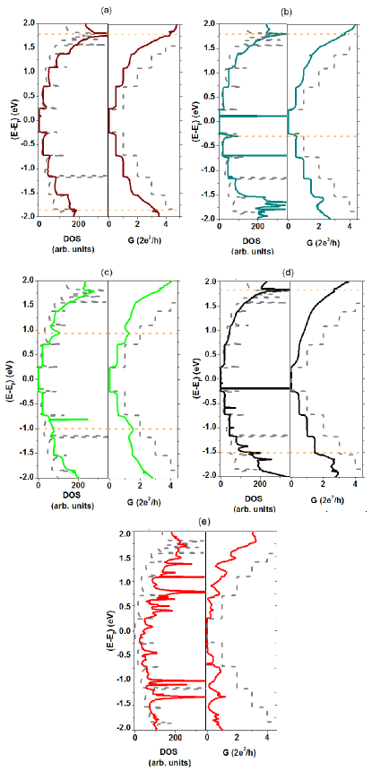
Each C atom from graphene lattice is capable of interaction with a single molecule and can be considered as a possible target for gas or vapour species resulting in ultrasensitive response Geim and Novoselov (2007); Basu and Bhattacharyya (2012). It was shown that the adsorption of gas molecule leads to the local change in the carrier concentration inducing a doping of the delocalized 2D electron gas, which can be experimentally measured in transistor like devices Pearce et al. (2011); Ohno, Maehashi, and Matsumoto (2010). Therefore, we have decided to test the possibility of detecting and distinguishing between very small concentrations of different simple organic molecules. In Fig. 2 we present DOS and transmission spectra of GML functionalized with five different types of adsorbates at the same concentration (two adsorbates): -CH3, -NH2, -NH, -OH, and -CH2 fragments. The band gap is clearly seen in all systems, because only 48 C atoms of scattering region were optimized, in such way, that C atoms adjacent electrode extensions have to perfectly match with those regions. Therefore, only at short range the graphene lattice can be affected by presence of the adsorbates and the structure is stressed (ca. 1.5 kbar). Impurity bands originating from attached groups are moved further from Fermi Energy and do not cross the Fermi level in the case of hydroxyl groups. However, even for those systems, it is possible to distinguish between systems with different adsorbates (Fig. 2) and its concentration (Fig. 1 (b)) from transmission spectra.
The -CH3 and -NH2 groups, as well as -NH radicals induce resonant transmission, whereas -OH anti-resonant transmission. The conductance peaks correspond with DOS peaks at -1.858 eV and 1.786 eV for -CH3 (see Fig. 2 (a)), at -0.295 eV and 1.798 eV for -NH2 (see Fig. 2 (b)), and at -1.004 eV and 0.932 eV for -NH radical (see Fig. 2 (c)). The adsorption of -OH groups leads to two small dips at -1.509 eV, and 1.823 eV corresponding with DOS peaks (see Fig. 2 (d)). These unique dips/peaks can be related with the type of adsorbates, because they are induced by quasi bond states in the structures. The sp2 sp3 rehybridization caused by the covalent bonding of the adsorbates to the basal plane of GML is responsible for this picture. Let us remark that the conductance of graphene functionalized with amines drops much slower with concentration of dopants than in the case of hydroxyl groups. It is mostly due to the fact that nitrogen acts as donor and has smaller electronegativity than oxygen. Transmission spectra of GML functionalized with -OH groups (Fig. 2 (d)) is much more smeared and asymmetrical around Fermi energy in comparison to pristine graphene and graphene functionalized with methyl group or amines. Hydroxyl group attracts electron cloud more efficiently than other considered adsorbates. However, it is the case of graphene functionalized with carbene that has a very different transmision spectra in comparison to pure graphene and to other considered attachments. The transmission coefficients at 0.4 eV are equal to 0.329 0.393, 0.483, 0.488, 0.508 for -CH2, -OH, -CH3, -NH2, -NH respectively. Adsorbates break the hexagonal symmetry of GML and create scattering centres. In other words, adsorbates act as a carrier trap reducing carrier density.
We have shown that different adsorbates lead to different energy of resonant and anti-resonant transmission. This effect was also shown by Wei et al. X.-L. Wei (2012) in the case of nitrogen-vacancy nanoribbons adsorbing NH2, CO and N2 molecules.
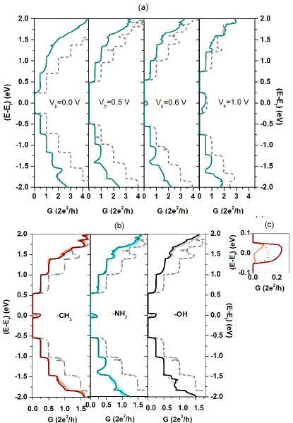
In Fig. 3 we have presented transmission spectra for non-zero bias voltage. Because of stress induced by fixing C atoms to perfectly match with those from electrode extensions, all studied systems have non-zero band gaps. The conductance gap broadens near the Fermi level under applied finite bias voltage Vb=0.5 V in comparison to zero-bias voltage case. After exceeding threshold voltage, transmission spectra change. For applied Vb=0.6 V, one can observe an appearance of a peak at Fermi level (see (Fig. 3 (a))) due to strong group and electrode coupling. For Vb=1.0 V, this peak is broadened, its amplitude is increased to almost one and becomes asymmetrical.
The spin-resolved transmissions spectra under Vb=0.6 V for all systems containing attachments with odd number of electrons (-OH, -NH2 and -CH3) are shown in Fig. 3 (b). Both, spin-up (darker curves) and spin-down (lighter curves) transmission spectra differ. Close to Fermi level conducting channel for one spin population is suppressed more than for other one. The most striking difference can be observed for -CH3 functionalized system, where electrons with spin-down will be almost fully filtered, whereas electrons with spin-up will be transmitted (see Fig. 3 (c)). In systems containing -OH,-NH2 and -CH3 groups the degeneracy is lifted under the influence of the functional group to the whole system. The functional groups significantly change charge distribution on graphene layer by dipolar field. Therefore, this influence of attachments on graphene layer can be understood by Stark effect.
Upon application of finite voltage, two spin components carry electric current through device in different extent. For Vb=0.6 V, the differences in current between two spin populations are equal to 0.307 A, 0.528 A, and 0.656 A for system containing two -NH2, -OH and -CH3 groups, respectively. The analysis of the conductance and current reveals that those systems can be used as supramolecular spin-filtering devices within some specific energy windows. Next step is to analyse changes in current-voltage characteristics induced by different adsorbates.
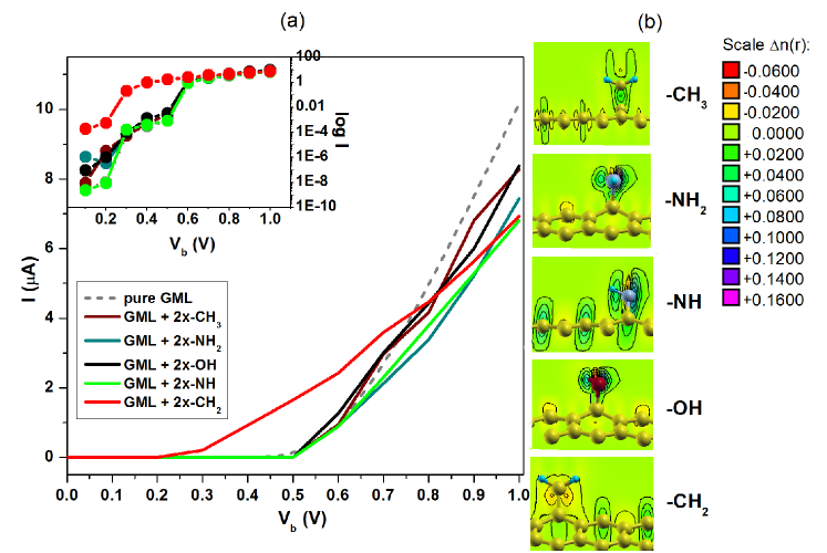
The calculated current-voltage characteristics (calculated using Eq. 3) for GMLs functionalized with -NH2, -NH, -CH3, -CH2 and -OH compared to the characteristics of the pristine GML (grey dashed line), are depicted in Fig. 4 (b). The critical voltage for the non-zero current is the lowest for GML functionalized with -CH2 radicals (0.2 V). Those adsorbates cause the most significant changes in current-voltage characteristics - the slope of non-zero part for -CH2 is 2.45 times smaller than for pristine graphene monolayer. The I(Vb) characteristics for other adsorbates and pure graphene are similar; current gradients for GML functionalized with -CH3, -OH, -NH2, and -NH are 1.27-1.58 times smaller than pure GML.
To better explain physical mechanism governing these effects, we have depicted in Fig. 4 (b) distribution of the changes of valence charge around adsorbates (side view) with the functionalized graphene lattice superimposed on. All studied types of adsorbates are strongly chemisorbed to the basal plane of graphene (see adsorption and strain energies in Tab. 1). Depending on the electronic configuration, the fragments form either single chemical bond to the C atom from the GL basal plane (-NH2, -CH3, and -OH), being in the so-called top position, or double bond (as -CH2 and -NH) with fragment’s C atom placed in the bridge positions. Incorporation of atoms with different level of electronegativity leads to different changes in local charge density. Therefore, functionalization with groups containing carbon slightly changes the situation in comparison to the pure graphene. Methyl group induces small positive valence electronic charge in the middle of the bond between basal plane and group, whereas carbene causes larger changes. One can clearly see areas of additional valence electronic charge more shifted to the adsorbate than to basal plane of graphene. For -CH2, there are also bigger changes in C-C bond in basal plane of graphene than for -CH3 group. Covalent functionalization with amines, -NH2 and -NH, leads mostly to generated excess charge at N atom. Again, the radical introduces more changes to the basal plane. In the case of hydroxyl group, the oxygen atoms introduce comparable positive difference of the valence pseudocharge density and the superposition of the atomic valence pseudocharge densities. However, the charge distribution disturbance caused by -CH2 radicals is the biggest one from studied examples of adsorbates. It is smeared over C atoms to which the radical is not directly bound (see the last DRHO of -CH2 functionalized graphene in Fig. 4 (b)).
Despite changes caused by functionalization it should be emphasized that the functionalized systems conduct comparable currents to pure system at the same bias voltage applied. At =1.0 V, the currents are equal to 10.160 A, 8.376 A, 8.274 A, 7.434 A, 6.937 A, and 6.808 A for pure GML, GML functionalized with -OH, -CH3, -NH2, -CH2, and -NH fragments, respectively. Covalent functionalization of GMLs does not ruin current flow through the system, as it is observed in the case of single walled carbon nanotubes (SWNT)Bouilly et al. (2011). Similar changes in current-voltage characteristics for armchair nanoribbons functionalized with -CH3 and -OH groups were presented in Ref. Tsuyuki, Sakamoto, and Tomiya (2012). It is worth to mention that our I(Vb) characteristics of functionalized GML look similar to experimental ones of reduced graphene oxide and graphene oxideSingh et al. (2011).
Generally, covalent functionalization, which is needed for sensing purposes, leads to a decrease of electrical conductivity. For fabrication of graphene based devices, such as sensors, the balance between conductivity and enhanced chemical reactivity should be carefully investigated. Our studies show that each kind of adsorbate and its concentration can be detected by its own unique resonant or anti-resonant peaks. Sensing substances in GML-based devices can be easily monitored through two-probe transport experiments. The GML are better candidates for building sensors than carbon nanotubes, where single walled nanotubes are not sufficient and usage of at least double walled nanotubes is required for proper operation of such devicesBouilly et al. (2011); Baraket et al. (2012).
IV Conclusions
We have shown that transport properties are affected by covalent functionalization. The transmission and I(Vb) characteristics differ between various types of attachments. The resonant/anti-resonant behaviours induced by quasi-bond states in the structures can be observed. Carbene introduces the most dramatic changes in transmission spectrum and current-voltage characteriscics, whereas methyl groups cause the smallest change. This effect allows one to distinguish between type and concentration of adsorbates with extremely high sensitivity. It should be emphasized that changes induced by functionalization are not dramatic in comparison with pristine GML. Therefore, functionalized graphene monolayers could be, in contrary to functionalized SWNTs, used as a channel in FET based sensors.
V Acknowledgement
This work has been supported by the European Founds for Regional Development within the SICMAT Project (Contact No. UDA-POIG.01.03.01-14-155/09). We acknowledge also support of the PL-Grid Infrastructure and of Interdisciplinary Centre for Mathematical and Computational Modeling, University of Warsaw (Grant No. G47-5). K. Z. Milowska acknowledges funding from the European Commission through the FP7-NMP programme (project UNION, grant No. 310250).
References
- Geim and Novoselov (2007) A. K. Geim and K. S. Novoselov, “The Rise of Graphene.” Nature Mater. 6, 183–191 (2007).
- Park and Ruoff (2009) S. Park and R. S. Ruoff, “Chemical Methods for the Production of Graphenes.” Nature Nanotech. 4, 217–224 (2009).
- Pacile et al. (2011) D. Pacile, J. C. Meyer, A. F. Rodryguez, M. Papagno, C. Gomez-Navarro, R. S. Sundaram, M. Burghard, K. Kern, C. Carbone, and U. Kaiser, “Electronic Properties and Atomic Structure of Graphene Oxide Membranes.” Carbon 49, 966 (2011).
- Sengupta et al. (2011) R. Sengupta, M. Bhattacharya, S. Bandyopadhyay, and A. K. Bhowmick, “A Review on the Mechanical and Electrical Properties of Graphite and Modified Graphite Reinforced Polymer Composites.” Progress in Polymer Science 36, 638–670 (2011).
- Georgakilas et al. (2012) V. Georgakilas, M. Otyepka, A. B. Bourlinos, V. Chandra, N. Kim, K. C. Kemp, P. Hobza, R. Zboril, and K. S. Kim, “Functionalization of Graphene: Covalent and Non-Covalent Approaches, Derivatives and Applications.” Chem. Rev. 112, 6156–6214 (2012).
- Luque et al. (2010) G. L. Luque, M. Rojas, G. Rivas, and E. Leiva, “The Origin of the Catalysis of Hydrogen Peroxide Reduction by Functionalized Graphene Surfaces: A Density Functional Theory Study.” Electrochimica Acta 56, 523–530 (2010).
- Neto et al. (2009) A. H. C. Neto, F. Guinea, N. M. R. Peres, K. S. Novoselov, and A. K. Geim, “The Electronic Properties of Graphene.” Rev. Mod. Phys. 81, 109–162 (2009).
- Sarma et al. (2011) S. D. Sarma, S. Adam, E. H. Hwang, and E. Rossi, “Electronic Transport in Two-Dimensional Graphene.” Rev. Mod. Phys. 83, 407–470 (2011).
- Kuila et al. (2012) T. Kuila, S. Bose, A. K. Mishra, P. Khanra, N. H. Kim, and J. H. Lee, “Chemical Functionalization of Graphene and Its Applications.” Progress in Materials Science 57, 1061–1105 (2012).
- Pramanik and Kang (2011) A. Pramanik and H. S. Kang, “Density Functional Theory Study of o2 and no Adsorption on Heteroatom-Doped Graphenes Including the van der Waals Interaction.” J. Phys. Chem. C 115, 10971–10978 (2011).
- Basu and Bhattacharyya (2012) S. Basu and P. Bhattacharyya, “Recent Developments on Graphene and Graphene Oxide Based Solid State Gas Sensors.” Sensors and Actuators B 173, 1–21 (2012).
- Pramanik and Kang (2010) A. Pramanik and H. S. Kang, “Colloquium: The Transport Properties of Graphene: An Introduction.” Rev. Mod. Phys. 82, 2673–2700 (2010).
- Mao et al. (2013) H. Y. Mao, Y. H. Lu, J. D. Lin, S. Zhong, A. T. S. Weeb, and W. Chen, “Manipulating the Electronic and Chemical Properties of Graphene via Molecular Functionalization.” Progress in Surface Science 88, 132–159 (2013).
- Liu, Liu, and Zhu (2011) H. Liu, Y. Liu, and D. Zhu, “Chemical Doping of Graphene.” J. Mater. Chem 21, 3335–3345 (2011).
- Schedin et al. (2007) F. Schedin, A. K. Geim, S. V. Morozov, E. W. Hill, P. Blake, M. I. Katsnelson, and K. S. Novoselov, “Detection of Individual Gas Molecules Adsorbed on Graphene.” Nature Mater. 6, 652 – 655 (2007).
- Wang et al. (2010) Y. Wang, Y. Shao, D. W. Matson, J. Li, and Y. Lin, “Nitrogen-Doped Graphene and Its Application in Electrochemical Biosensing.” ACS Nano 4, 1790–1798 (2010).
- Liu et al. (2010) Y. Liu, D. Yu, C. Zeng, Z. Miao, and L. Dai, “Biocompatible Graphene Oxide-Based Glucose Biosensors.” Langmuir 26, 6158–6160 (2010).
- Ang et al. (2008) P. K. Ang, W. Chen, A. T. S. Wee, and K. P. Loh, “Solution-Gated Epitaxial Graphene as pH Sensor.” J. Am. Chem. Soc. 130, 14392–14393 (2008).
- Lu et al. (2009) C.-H. Lu, H.-H. Yang, C.-L. Zhu, X. Chen, and G.-N. Chen, “A Graphene Platform for Sensing Biomolecules.” Angew. Chem. Int. Ed 48, 4785–4787 (2009).
- Mohanty and Berry (2008) N. Mohanty and V. Berry, “Graphene-Based Single-Bacterium Resolution Biodevice and DNA Transistor: Interfacing Graphene Derivatives with Nanoscale and Microscale Biocomponents.” Nano Lett. 8, 4469–4476 (2008).
- Chang et al. (2013) J. Chang, S. Mao, Y. Zhang, S. Cui, G. Zhou, X. Wu, C.-H. Yang, and J. Chen, “Ultrasonic-Assisted Self-Assembly of Monolayer Graphene Oxide for Rapid Detection of Escherichia Coli Bacteria.” Nanoscale 5, 3620–3626 (2013).
- Shao et al. (2010) Y. Shao, J. Wang, H. Wu, J. Liu, I. A. Aksay, and Y. Lina, “Graphene Based Electrochemical Sensors and Biosensors: A Review.” Electroanalysis 22, 1027–1036 (2010).
- Kehayias et al. (2013) C. E. Kehayias, S. MacNaughton, S. Sonkusale, and C. Staii, “Kelvin Probe Microscopy and Electronic Transport Measurements in Reduced Graphene Oxide Chemical Sensors.” Nanotechnology 24, 245502 (2013).
- Li, Cao, and Hu (2012) N. Li, M. Cao, and C. Hu, “Review on the Latest Design of Graphene-Based Inorganic Materials.” Nanoscale 4, 6205–6218 (2012).
- Erni et al. (2010) R. Erni, M. D. Rossell, M.-T. Nguyen, S. Blankenburg, D. Passerone, P. Hartel, N. Alem, K. Erickson, W. Gannett, and A. Zettl, “Stability and Dynamics of Small Molecules Trapped on Graphene.” Phys. Rev. B 82, 165443 (2010).
- Boukhvalov and Katsnelson (2009) D. W. Boukhvalov and M. I. Katsnelson, “Chemical Functionalization of Graphene.” J. Phys.: Condens. Matter 21, 344205 (2009).
- Boukhvalov and Katsnelson (2010) D. W. Boukhvalov and M. I. Katsnelson, “A New Route Towards Uniformly Functionalized Single-Layer Graphene.” J. Phys. D: Appl. Phys. 43, 175302 (2010).
- Milowska, Birowska, and Majewski (2011) K. Z. Milowska, M. Birowska, and J. A. Majewski, “Structural and Electronic Properties of Functionalized Graphene.” Acta Physica Polonica A 120, 842–844 (2011).
- Milowska, Birowska, and Majewski (2012) K. Z. Milowska, M. Birowska, and J. A. Majewski, “Mechanical and Electrical Properties of Carbon Nanotubes and Graphene Layers Functionalized with Amines.” Diamond and Related Materials 23, 167–171 (2012).
- Milowska and Majewski (2013) K. Z. Milowska and J. A. Majewski, “Stability and Electronic Structure of Covalently Functionalized Graphene Layers.” Physica Status Solidi B 250, 1474–1477 (2013).
- Datta (1995) S. Datta, Electronic Transport in Mesoscopic Systems (Cambridge University Press, 1995).
- Brandbyge et al. (2002) M. Brandbyge, J. L. Mozos, P. Ordejon, J. Taylor, and K. Stokbro, “Density-Functional Method for Nonequilibrium Electron Transport.” Phys. Rev. B 65, 165401 (2002).
- Ordejon, Artacho, and Soler (1996) P. Ordejon, E. Artacho, and J. M. Soler, “Self-Consistent Order-N Density-Functional Calculations for Very Large Systems.” Phys. Rev. B 53, R10441–R10444 (1996).
- Soler et al. (2002) J. M. Soler, E. Artacho, J. D. Gale, A. Garcia, J. Junquera, P. Ordejon, and D. Sanchez-Portal, “The SIESTA Method for Ab Initio Order-N Materials Simulation.” J. Phys.: Condens. Matter 14, 2745 (2002).
- Sanchez-Portal et al. (1997) D. Sanchez-Portal, P. Ordejon, E. Artacho, and J. M. Soler, “Density-Functional Method for Very Large Systems with LCAO Basis Sets.” Int. J. Quant. Chem. 65, 453–461 (1997).
- Perdew, Burke, and Ernzerhof (1996) J. P. Perdew, K. Burke, and M. Ernzerhof, “Generalized Gradient Approximation Made Simple.” Phys. Rev. Lett. 77, 3865–3868 (1996).
- Baraket et al. (2012) M. Baraket, R. Stine, W. K. Lee, J. T. Robinson, C. R. Tamanaha, P. E. Sheehan, and S. G. Walton, “Aminated Graphene for DNA Attachment Produced via Plasma Functionalization.” App. Phys. Lett. 100, 233123 (2012).
- Garcia-Lastra et al. (2008) J. M. Garcia-Lastra, K. S. Thygesen, M. Strange, and A. Rubio, “Conductance of Sidewall-Functionalized Carbon Nanotubes: Universal Dependence on Adsorption Sites.” Phys. Rev. Lett. 101, 236806 (2008).
- Garcia-Lastra (2010) J. M. Garcia-Lastra, “Strong Dependence of Band-gap Opening at the Dirac Point of Graphene upon Hydrogen Adsorption Periodicity.” Phys. Rev. B 82, 235418 (2010).
- Topsakal et al. (2010) M. Topsakal, V. M. K. Bagci, , and S. Ciraci, “Current-voltage (I-V) Characteristics of Armchair Graphene Nanoribbons under Uniaxial Strain.” Phys. Rev. B 81, 205437 (2010).
- Wu et al. (2013) G.-X. Wu, Z.-Q. Wang, Y.-H. Jing, and C.-Y. Wang, “I-V Curves of Graphene Nanoribbons under Uniaxial Compressive and Tensile Strain.” Chem. Phys. Lett. 559, 82–87 (2013).
- Pearce et al. (2011) R. Pearce, T. Iakimov, M. Andersson, L. Hultman, A. L. Spetz, and R. Yakimova, “Epitaxially Grown Graphene Based Gas Sensors for Ultra Sensitive no2 Detection.” Sensors and Actuators: B 155, 451–455 (2011).
- Ohno, Maehashi, and Matsumoto (2010) Y. Ohno, K. Maehashi, and K. Matsumoto, “Chemical and Biological Sensing Applications Based on Graphene Field-Effect Transistors.” Biosensors and Bioelectronics 26, 1727–1730 (2010).
- X.-L. Wei (2012) J.-X. Z. X.-L. Wei, Y.-P. Chen W.-L. Liu, “Enhanced Gas Sensor Based on Nitrogen-Vacancy Graphene Nanoribbons.” Phys. Lett. A 376, 559–562 (2012).
- Bouilly et al. (2011) D. Bouilly, J. Cabana, F. Meunier, M. Desjardins-Carriere, F.Lapointe, P. Gagnon, F. L. Larouche, E. Adam, M. Paillet, , and R. Martel, “Wall-Selective Probing of Double-Walled Carbon Nanotubes Using Covalent Functionalization.” ACS Nano 5, 4927–4934 (2011).
- Tsuyuki, Sakamoto, and Tomiya (2012) H. Tsuyuki, S. Sakamoto, and M. Tomiya, “Electron Transfer on Impurity Doped Graphene Nanoribbon.” Journal of Physics: Conference Series 402, 012016 (2012).
- Singh et al. (2011) V. Singh, D. Joung, L.Zhai, S. Das, S. I. Khondaker, and S. Seal, “Graphene Based Materials: Past, Present and Future,” Progress in Materials Science 56, 1178–1271 (2011).