Competing Channels for Hot Electron Cooling in Graphene
Abstract
We report on temperature dependent photocurrent measurements of high-quality dual-gated monolayer graphene (MLG) p-n junction devices. A photothermoelectric (PTE) effect governs the photocurrent response in our devices, allowing us to track the hot electron temperature and probe hot electron cooling channels over a wide temperature range (4 K to 300 K). At high temperatures (), we found that both the peak photocurrent and the hot spot size decreased with temperature, while at low temperatures (), we found the opposite, namely that the peak photocurrent and the hot spot size increased with temperature. This non-monotonic temperature dependence can be understood as resulting from the competition between two hot electron cooling pathways: (a) (intrinsic) momentum-conserving normal collisions (NC) that dominates at low temperatures and (b) (extrinsic) disorder-assisted supercollisions (SC) that dominates at high temperatures. Gate control in our high quality samples allows us to resolve the two processes in the same device for the first time. The peak temperature depends on carrier density and disorder concentration, thus allowing for an unprecedented way of controlling graphene’s photoresponse.
Slow electron-lattice thermal equilibration is responsible for a plethora of new optoelectronic Xu et al. (2010); Song et al. (2011); Gabor et al. (2011); Sun et al. (2012), transport Song and Levitov (2012); Song et al. (2013), and thermoelectronic Betz et al. (2013); Cho et al. (2013) phenomena in graphene. The wide temperature ranges (lattice temperature, 4 K to 300 K) and long spatial scales in which hot carriers proliferate make graphene an ideal candidate for electronic energy transduction and numerous applications. Central to these are the unusual electron-phonon scattering pathways that dominate the cooling channels of graphene Bistritzer and MacDonald (2009); Song et al. (2012); Betz et al. (2013); Graham et al. (2013a); Tielrooij et al. (2013); Shi et al. (2014).
Unlike other materials, electron-lattice cooling at room temperature in graphene is dominated by an extrinsic three-body process Song et al. (2012). This occurs when acoustic phonon emission is assisted by disorder scattering, as is called supercollisions (SC). SC dominates over the intrinsic momentum-conserving emission of acoustic phonons (NC) for high temperatures. At low temperatures, the intrinsic process is expected to be dominant. However, the intrinsic NC process has never been experimentally observed before Graham et al. (2013a, b).
Here, we report on temperature dependent spatially resolved photocurrent measurements of high-quality MLG p-n junction devices. At the p-n interface, the PTE effect dominates the photocurrent generation Song et al. (2011); Gabor et al. (2011); Sun et al. (2012) and exhibits a non-monotonic temperature dependence. We demonstrate that both the magnitude and spatial extent of the photoresponse are highly enhanced at an intermediate temperature , indicating the coexistence of momentum-conserving NC cooling and disorder-assisted SC mechanisms. NC (SC) cooling dominates below (above) , which can be tuned by varying the charge and impurity densities. In addition, we observed that the photoresponse at the graphene-metal (G-M) interface is also dominated by the PTE effect with a similar temperature dependent behavior. Lastly, we show that the dramatic suppression of hot carrier cooling at allows for non-local control of hot carrier dynamics. This involves top gate modulation of the photocurrent arising from illuminating the (distant) G-M interface.

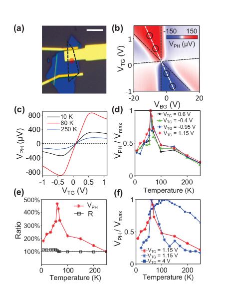
Our MLG p-n junction devices are fabricated by micromechanical exfoliation, followed by standard e-beam lithography techniques to define contacts (Fig. 1a). Hexagonal boron nitride flakes (-nm thick) are then placed onto the samples as dielectric insulators by using a PMMA-transfer method, after which local top gates are fabricated to form p-n junctions in the center of the devices. In our experiments, the samples are kept in a liquid helium flow cryostat with an embedded resistive heater to give a precise temperature control from 4 K to above room temperature. We have measured 8 -supported exfoliated MLG devices with a high mobility of , all of which show similar results. The data presented in this paper was collected from two of them: Device 1 (8 m long) and Device 2 (6 m long).
By tuning back gate () and top gate () voltages independently, the junction can be operated in four different charge configurations: p-p, n-n, p-n and n-p Williams et al. (2007); Özyilmaz et al. (2007); Huard et al. (2007); Gabor et al. (2011); Sun et al. (2012). The photovoltage measured with the laser fixed at the p-n interface as a function of and exhibits six regions of alternating signs (Fig. 1b), which has been shown to be the fingerprint of the PTE effect Song et al. (2011); Gabor et al. (2011); Sun et al. (2012). This six-fold pattern is observed over a wide range of lattice (environment) temperatures from K up to K. Fig. 1c shows slices of the photovoltage plot for (dashed white line in Fig. 1b) at three representative temperatures (K, K and K), where and are the chemical potentials in the single- and dual-gated regions, respectively. All three slices exhibit similar qualitative dependence on charge density, but the slice representing the intermediate temperature (K) is the greatest in magnitude, indicating a non-monotonic dependence on temperature.
A detailed investigation of the relationship between photovoltage and lattice temperature is shown in Fig. 1d, where is plotted as a function of temperature at four different points (circles) along the slice in Fig. 1b, all of which exhibit a dramatic enhancement at K. In comparison, only minor differences are observed for the measured resistance, , within the same temperature range. We plot (same as the red line in Fig. 1d) and (near the Dirac point) as a function of temperature in the same graph (Fig. 1e). Both and are normalized by their lowest values, which occur at K. While shows an increase by as much as at , stays fairly constant over the full temperature range (similar for measured away from the Dirac point). In Fig. 1f, we show the temperature dependence of collected from Device 2 at low (blue star) and high (blue square) densities, both of which exhibit non-monotonic behaviors but with an upwards shift of from low to high density.
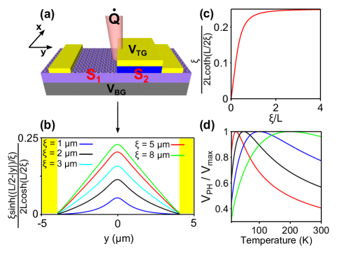
This non-monotonic temperature dependence of the photoresponse is closely related to hot electron dynamics in graphene. To illustrate this, we begin by describing the photovoltage as which determines the open-circuit PTE voltage generated from a sharply defined p-n junction Song et al. (2011); Gabor et al. (2011) ( is the electronic temperature increase at the p-n interface). We assume a linear response regime where Gabor et al. (2011) ( is the lattice temperature) in the following analysis, which is consistent with the fact that all the measurements are performed in the linear power regime. By neglecting the temperature dependence of the resistance, is linear in Zuev et al. (2009); Wei et al. (2009), indicating a strong temperature dependence embedded in .

With the laser focused on the p-n interface, a steady-state spatial profile of the electronic temperature is established (Fig. 2a and 2b). Material parameters that can affect the profile include the thermal conductivity , the electronic specific heat , and the electron-lattice cooling rate . The combination of these three parameters generates a characteristic cooling length for hot carrier propagation in the system Song et al. (2011). Due to the linear temperature dependence of both (Wiedemann-Franz law) and , the temperature dependence of is embedded in . The analytical solution to the heat equation of the system is (See Supplementary Information), where is the rate at which heat enters the system and is the device length ( is the value at ). Fig. 2b shows the spatial profile of in units of , i.e., the dimensionless quantity , for different values of . The linear temperature dependence of cancels out that of in the denominator of when we multiply these to find the photoresponse . Consequently, the whole temperature dependence of is through and thus ultimately via the cooling rate only. As can be seen from Fig. 2c, the photoresponse, which is proportional to , grows quickly with () and becomes saturated when approaches the system length .
In order to understand the temperature dependence of , we consider possible hot carrier cooling pathways in graphene. After initial relaxation of photo-excited carriers due to electron-electron scattering and optical phonon emission, the hot carrier distribution cools by emitting acoustic phonons Bistritzer and MacDonald (2009). A relevant cooling process is single acoustic phonon emission (NC), which gives a slow cooling rate with a prefactor related to the charge density Bistritzer and MacDonald (2009). However, the disorder-assisted SC cooling gives rise to a competing cooling channel with a different cooling rate , where the prefactor is related to the amount of disorder and the charge density Song et al. (2012). Therefore, NC and SC dominate at low and high temperatures respectively, with a cross-over temperature Song et al. (2012), where is the Bloch-Grneisen temperature, and is the disorder-dependent mean free path as modeled in Ref. Song et al. (2012).
We see from the above equation that the optimal temperature for photodetection can be tuned by the disorder concentration (via ) and the charge carrier density (via ), which can be understood in terms of the relative weight of NC and SC cooling pathways. The available phase space for NC cooling is expanded when increasing the charge carrier density, and the SC channel is suppressed by reducing the disorder concentration. Both changes result in an increase in the temperature range dominated by NC and a decrease in the range of SC behavior, which will cause to increase. On the other hand, decreasing the carrier density and increasing the disorder amount will cause to shift to lower temperatures. The shifting of due to carrier density change is shown in Fig. 1f and Fig. 2d (simulation). To further verify the disorder relation, in-situ and systematic control of the disorder concentration is required. More detailed work needs to be done to uncover what type of disorder is dominant in assisting hot electron cooling. In any case, we want to emphasize that less disorder is always preferable in terms of the absolute efficiency of photocurrent at any temperatures.
The sensitivity of to the charge density and disorder concentration may account for the different (monotonic) temperature dependent behavior observed in previous studies Dawlaty et al. (2008); George et al. (2008); Plochocka et al. (2009); Xu et al. (2010); Strait et al. (2011); Sun et al. (2012); Winnerl et al. (2011); Graham et al. (2013a, b). In addition, all the above arguments are based on the condition, while otherwise we need to consider the full expression of the relative cooling weight between the SC and NC, which is derived in Ref. Song et al. (2012) as . The overheating of electrons () will strongly enhance the SC weight even at low lattice temperatures, completely masking the NC processes.
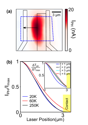
The non-monotonic temperature dependence of hot electron cooling is reflected not only in the magnitude of the photocurrent, but also in its spatial profile. Fig. 3a shows the spatially resolved photocurrent microscopy () of Device 2. A strong photocurrent signal is observed at the p-n interface while the contact signals are strongly suppressed, which allows for independent extraction of the p-n signal profile. This signal decays with distance away from the p-n edge (denoted by a dashed black arrow in Fig. 3a) at different rates depending on temperature (Fig. 3b). The lowest decay rate is observed at the peak temperature K, corresponding to the longest cooling length (theoretical simulations in Fig. 3b inset).


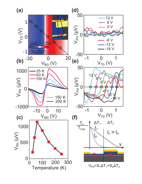
We now turn to the G-M interface of Device 1, where we also see evidence of a PTE response to laser illumination. In order to avoid ambiguity, we fixed the laser at the interface away from the top gate electrode. Fig. 4a shows the photovoltage as a function of and at 250 K, exhibiting complete reversal of polarity with respect to , which is consistent with previous studies Lee et al. (2008); Park et al. (2009); Mueller et al. (2009); Xia et al. (2009). Fig. 4b plots slices as a function of (fixed ) at various temperatures, showing once again that the photovoltage is maximized at an intermediate temperature (60 K) and thus has a non-monotonic temperature dependence. The full temperature dependent behavior of is shown in Fig. 4c, where the maximum values of are plotted against temperature. We emphasize that this non-monotonic temperature dependence due to the hot electron cooling is unique to the PTE response and is not expected from the conventional photovoltaic (PV) effect, in which the seperation of excited carriers by the built-in electric field leads to a net current Lee et al. (2008); Park et al. (2009); Mueller et al. (2009); Xia et al. (2009). Therefore, this serves as a strong indication that the PTE effect dominates the response to laser illumination of the G-M interface, consistent with recent reports where the photovoltaic contribution at 800 nm wavelength is relatively small Echtermeyer et al. (2014).
Another important fact that can be extracted from Fig. 4a is that exhibits very little dependence on at K. This is shown more clearly in Fig. 4d, where is plotted as a function of at different back gate voltages (vertical slices of Fig. 4a). Each curve has been subtracted by the value along the diagonal dashed line in Fig. 4a, which defines the charge neutrality point of the dual-gated region. Indeed, no obvious top gate dependence is observable other than random fluctuations. In striking contrast, the same plot as Fig. 4d, but at the peak temperature K instead, exhibits clear top gate modulation (Fig. 4e), indicating nonlocal hot carrier transport enhanced by a long cooling length.
This is further illustrated in Fig. 4f. When the cooling length is short either due to NC at low temperature or SC at high temperature, the hot carriers strongly thermalize with the lattice before reaching the top-gated region. This results in a low temperature gradient and thus a low PTE voltage in that region. Therefore, it is difficult to observe the modulation of by the top gate. In contrast, at the peak temperature , the energy loss from the electronic system to the lattice is minimized. Hot carriers feature long relaxation lifetimes and long spatial propagation, leading to a considerable to drive . In this regime, the top gate modulation is readily observable (Fig. 4e).
In conclusion, we have observed a strong non-monotonic temperature dependent behavior of the PTE response of high quality graphene p-n and G-M junctions. This behavior originates from two competing mechanisms for hot carrier cooling. At the peak temperature, hot carriers cool the slowest, resulting in a 5-fold increase in the photocurrent generation with respect to room temperature and a dramatic nonlocal phenomenon. This optimal temperature for maximal hot carrier extraction is controllable by carrier density and disorder concentration, which may pave the way for the design of more efficient graphene hot carrier devices.
We thank J. C. W. Song and L. S. Levitov for numerous fruitful discussions. This work has been supported by AFOSR grant number FA9550-11-1-0225 (measurement and data analysis) and a Packard Fellowship. Device fabrication was supported by a seed fund from S3TEC, an Energy Frontier Research Center funded by DOE, Office of Science, BES under Award number DE-SC0001299/DE-FG02-09ER46577. This work made use of the Materials Research Science and Engineering Center Shared Experimental Facilities supported by the National Science Foundation (NSF) (award no. DMR-0819762) and of Harvard′s Center for Nanoscale Systems, supported by the NSF (grant ECS-0335765).
References
- Xu et al. (2010) X. Xu, N. M. Gabor, J. S. Alden, A. M. van der Zande, and P. L. McEuen, Nano Lett. 10, 562 (2010).
- Song et al. (2011) J. C. W. Song, M. S. Rudner, C. M. Marcus, and L. S. Levitov, Nano Lett. 11, 4688 (2011).
- Gabor et al. (2011) N. M. Gabor, J. C. W. Song, Q. Ma, N. L. Nair, T. Taychatanapat, K. Watanabe, T. Taniguchi, L. S. Levitov, and P. Jarillo-Herrero, Science 334, 648 (2011).
- Sun et al. (2012) D. Sun, G. Aivazian, A. M. Jones, J. S. Ross, W. Yao, D. Cobden, and X. Xu, Nat. Nanotechnol. 7, 114 (2012).
- Song and Levitov (2012) J. C. W. Song and L. S. Levitov, Phys. Rev. Lett. 109, 236602 (2012).
- Song et al. (2013) J. C. W. Song, D. A. Abanin, and L. S. Levitov, Nano Lett. 13, 3631 (2013).
- Betz et al. (2013) A. C. Betz, S. H. Jhang, E. Pallecchi, R. Ferreira, G. Feve, J.-M. Berroir, and B. Placais, Nat. Phys. 9, 109 (2013).
- Cho et al. (2013) S. Cho, S. D. Kang, W. Kim, E.-S. Lee, S.-J. Woo, K.-J. Kong, I. Kim, H.-D. Kim, T. Zhang, J. A. Stroscio, et al., Nat. Mat. 12, 913 (2013).
- Bistritzer and MacDonald (2009) R. Bistritzer and A. H. MacDonald, Phys. Rev. Lett. 102, 206410 (2009).
- Song et al. (2012) J. C. W. Song, M. Y. Reizer, and L. S. Levitov, Phys. Rev. Lett. 109, 106602 (2012).
- Graham et al. (2013a) M. W. Graham, S.-F. Shi, D. C. Ralph, J. Park, and P. L. McEuen, Nat. Phys. 9, 103 (2013a).
- Tielrooij et al. (2013) K. J. Tielrooij, J. C. W. Song, S. A. Jensen, A. Centeno, A. Pesquera, A. Zurutuza Elorza, M. Bonn, L. S. Levitov, and F. H. L. Koppens, Nat. Phys. 9, 248 (2013).
- Shi et al. (2014) S.-F. Shi, T.-T. Tang, B. Zeng, L. Ju, Q. Zhou, A. Zettl, and F. Wang, Nano Letters 14, 1578 (2014).
- Graham et al. (2013b) M. W. Graham, S.-F. Shi, Z. Wang, D. C. Ralph, J. Park, and P. L. McEuen, Nano Lett. 13, 5497 (2013b).
- Williams et al. (2007) J. R. Williams, L. DiCarlo, and C. M. Marcus, Science 317, 638 (2007).
- Özyilmaz et al. (2007) B. Özyilmaz, P. Jarillo-Herrero, D. Efetov, D. A. Abanin, L. S. Levitov, and P. Kim, Phys. Rev. Lett. 99, 166804 (2007).
- Huard et al. (2007) B. Huard, J. A. Sulpizio, N. Stander, K. Todd, B. Yang, and D. Goldhaber-Gordon, Phys. Rev. Lett. 98, 236803 (2007).
- Zuev et al. (2009) Y. M. Zuev, W. Chang, and P. Kim, Phys. Rev. Lett. 102, 096807 (2009).
- Wei et al. (2009) P. Wei, W. Bao, Y. Pu, C. N. Lau, and J. Shi, Phys. Rev. Lett. 102, 166808 (2009).
- Dawlaty et al. (2008) J. M. Dawlaty, S. Shivaraman, M. Chandrashekhar, F. Rana, and M. G. Spencer, Applied Physics Letters 92, 042116 (2008).
- George et al. (2008) P. A. George, J. Strait, J. Dawlaty, S. Shivaraman, M. Chandrashekhar, F. Rana, and M. G. Spencer, Nano Letters 8, 4248 (2008).
- Plochocka et al. (2009) P. Plochocka, P. Kossacki, A. Golnik, T. Kazimierczuk, C. Berger, W. A. de Heer, and M. Potemski, Phys. Rev. B 80, 245415 (2009).
- Strait et al. (2011) J. H. Strait, H. Wang, S. Shivaraman, V. Shields, M. Spencer, and F. Rana, Nano Lett. 11, 4902 (2011).
- Winnerl et al. (2011) S. Winnerl, M. Orlita, P. Plochocka, P. Kossacki, M. Potemski, T. Winzer, E. Malic, A. Knorr, M. Sprinkle, C. Berger, et al., Phys. Rev. Lett. 107, 237401 (2011).
- Lee et al. (2008) E. J. H. Lee, K. Balasubramanian, R. T. Weitz, M. Burghard, and K. Kern, Nat. Nanotechnol. 3, 486 (2008).
- Park et al. (2009) J. Park, Y. H. Ahn, and C. Ruiz-Vargas, Nano Lett. 9, 1742 (2009).
- Mueller et al. (2009) T. Mueller, F. Xia, M. Freitag, J. Tsang, and P. Avouris, Phys. Rev. B 79, 245430 (2009).
- Xia et al. (2009) F. Xia, T. Mueller, R. Golizadeh-Mojarad, M. Freitag, Y.-m. Lin, J. Tsang, V. Perebeinos, and P. Avouris, Nano Letters 9, 1039 (2009).
- Echtermeyer et al. (2014) T. J. Echtermeyer, P. S. Nene, M. Trushin, R. V. Gorbachev, A. L. Eiden, S. Milana, Z. Sun, J. Schliemann, E. Lidorikis, K. S. Novoselov, et al., arXiv: 1402.1266 (2014).