Gain Stabilization of SiPMs111Work supported by EC as INFRA project no. 262025, AIDA
Jaroslav Cvachb222Work supported by the Ministry of Education, Youth and Sports, Czech Republic, project LG130131, Gerald Eigena333Work supported by the Norwegian Research Council, Jiri Kvasnickab, Ivo Polakb, Erik van der Kraiija and Justas Zalieckasa
aDepartment of Physics,
University of Bergen, N-5007 Bergen, Norway
bInstitute of Physics (FZU), Prague, Czech Republic
The gain of SiPMs depends both on bias voltage and on temperature. For stable operations, both need to be kept constant. In an ILC calorimeter with millions of channels, this is a challenging task. It is, therefore, desirable to compensate for temperature variations by automatically readjusting the bias voltage. We have designed a bias voltage regulator board to achieve this task. We anticipate an uncertainty on the gain stability at the level of . First, we present measurements of the gain dependence on temperature and bias voltage for several SiPMs from three different manufacturers and determine their dV/dT dependence. Next, we demonstrate the performance of the gain stability with the bias voltage regulator test board on four SiPMs.
PRESENTED AT
International Workshop on Future Linear Colliders, LCWS13
Tokyo, Japan, 11–15 November 2013
1 Introduction
The analog hadron calorimeter (AHCAL) is one possible hadron calorimeter option for a detector operating at the international linear collider. It consists of a 30-layer steel plate scintillator tile array [1]. The scintillator tiles are read out with SiPMs [2, 3, 4] whose gain depends on both bias voltage and on temperature . With increasing temperature, the gain decreases while with increasing bias voltage the gain increases. For stable operations, we need to keep the gain constant. In test beam measurements of the AHCAL physics prototype, we have corrected the gain for temperature variations offline. In a real detector with millions of channels, this is not a viable option. However, we can correct for gain changes induced by temperature variations by readjusting the bias voltage. Thus, our goal is to build a bias voltage regulator that stabilizes the gain at a level of . First, we need to measure the gain dependence versus temperature and bias voltage to extract dV/dT. Next, we build a bias voltage regulator test board that provides the appropriate bias voltage readjustment when the temperature changes. This work is conducted in the framework of the EU project AIDA [5].
2 Test Setup
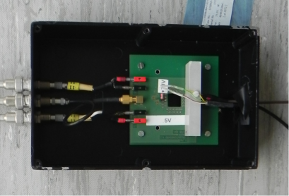
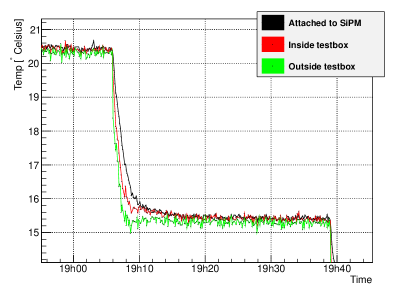
We perform all measurements at CERN in a climate chamber that is accurate to . The SiPM is mounted inside a black metal box that also houses a preamplifier, a blue LED and temperature sensors. The preamplifier provides a gain of 8.9. The SiPM signal is recorded with a digital oscilloscope that is read out by a PC. This readout scheme was used in the T3B test beam studies [6, 7]. We shine 2 ns long LED pulses on the SiPM. We measure the temperature with three pt 1000 sensors, one close to the SiPM, another one in the black box and a third one in the climate chamber. In addition, an LM35 sensor placed near the SiPM is used by the bias voltage regulator for performing the bias voltage readjustments. We vary T from to in steps of , except for the range where we use steps of . We take 50,000 events per run at a fixed temperature. The temperature at the SiPM and the preset temperature differ by an offset of , which remains unchanged over the entire range. Figure 1 shows temperature profiles of the pt 1000 temperature sensors after reducing the preset temperature by . We start a new run once the temperature reaches equilibrium, which typically takes about 15 min.
We have measured the dependence versus and the dependence versus for 15 SiPMs from three manufacturers (Hamamatsu, KETEK and CPTA). Table 1 lists their properties. The CPTA SiPMs were attached to a scintillator tile. While all Hamamatsu and KETEK detectors could be illuminated directly by the blue LED, we tried to shine the LED light onto the CPTA SIPMs as closely as possible. We selected four of them (CPTA 857, CPTA 1677, KETEK W 12 and Hamamatsu 11759) to demonstrate the performance of the bias voltage readjustment with the bias voltage regulator test board.
| Manufacturer | Sensitive | Pixel | Nominal | Typical | Serial | |
| and Type | area | pitch | pixels | G | ||
| [V] | ||||||
| Hamamatsu | ||||||
| S10943-8584(X) | 400 | 71.69 | 7.49 | 11759 | ||
| S10943-8584(X) | 400 | 71.57 | 7.49 | 11766 | ||
| S10943-8584(X) | 400 | 71.50 | 7.48 | 11770 | ||
| S10943-8584(X) | 400 | 71.33 | 7.48 | 11771 | ||
| Sample A | 2500 | A1 | ||||
| Sample B | 2500 | B1 | ||||
| Sample A | 4440 | A2 | ||||
| Sample B | 4440 | B2 | ||||
| CPTA | ||||||
| 796 | 33.4 | 7.1 | 857 | |||
| 796 | 33.1 | 6.3 | 922 | |||
| 796 | 33.3 | 6.3 | 975 | |||
| 796 | 33.1 | 7.0 | 1065 | |||
| 796 | 33.3 | 14.6 | 1677 | |||
| KETEK | ||||||
| MP15 V6 | 15 | 4384 | W8 | |||
| MP20 V4 | 20 | 12100 | W12 |
3 Layout of the Voltage Regulator Test Board
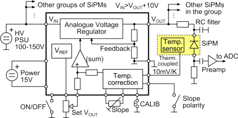
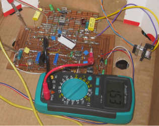
Figure 2 (left) shows the schematic layout of the bias voltage regulator test board and Fig. 2 (right) shows a photograph of it. The bias voltage regulator is designed to operate in the to region plus temperature correction effects. The temperature slope is variable from to , both for positive and negative values.
4 Gain Determination
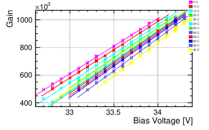
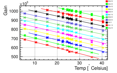
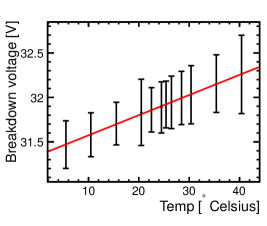
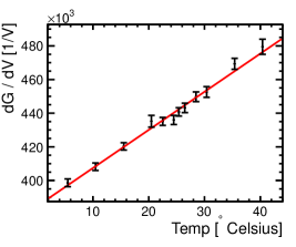
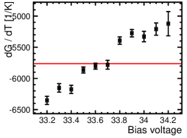
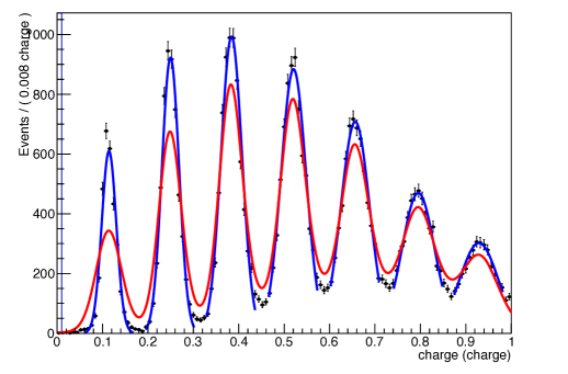
Figure 3 shows a spectrum of single photoelectron peaks recorded with the Hamamatsu MPPC 11759. The red curve represents a Gaussian multi-kernel function and the blue curves show Gaussian fits of the individual photoelectron peaks. We accept only runs for which the results of the two fit methods agree within . The gain is the distance between the pedestal peak and the first photoelectron peak. The distance between successive photoelectron peaks should be same. However, we noticed that the distance between first photoelectron peak and pedestal is slightly smaller than that between first and second photoelectron peaks. Since individual photoelectron peaks are clearly visible in Hamamatsu MPPCs, we define the gain here as the difference between the first and second photoelectron peaks. For the KTEK and CPTA detectors, the second photoelectron peak is often not clearly visible. Therefore, we define the gain for these SiPMs as the distance between the pedestal and the first photoelectron peak. The error on the gain is determined from the uncertainties of the two fitted Gaussian peak positions added in quadrature.
For each SiPM, we measure the gain dependence on bias voltage at a fixed temperature. Each data point is determined from 50,000 80 ns long waveforms. Figure 4 (left) shows the measurements of the gain versus bias voltage for SiPM CPTA 857. For each temperature, we fit the measured points with a first-order polynomial to extract the breakdown voltage and the slope . Figure 5 (left) depicts the dependence of breakdown voltage versus temperature. We observe a linear increase of the breakdown voltage with temperature. For example at and , we measure a gain of and a breakdown voltage of The slope is proportional to the capacitance of the SiPM. Figure 5 (middle) depicts the dependence on temperature. We see that the detector capacitance rises with temperature. This effect is clearly visible for most of the 15 SiPMs tested and has been observed in other studies [8]. A possible explanation is that the depletion zone in the high-gain region decreases with , which in turn leads to an increase of the capacitance. We need to perform more tests to check this hypothesis.
We fit the temperature dependence of with a zeroth-order polynomial and a first-order polynomial. The zeroth-order polynomial yields while a linear fits yields an offset of . Since these values are in perfect agreement, we use the result from the zeroth-order polynomial fit to extract .
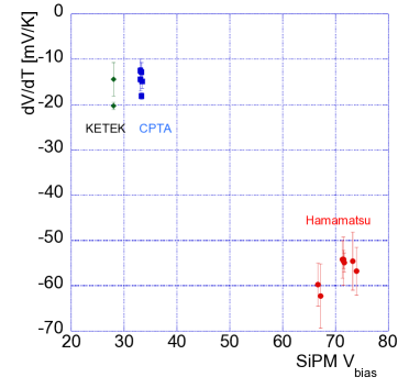
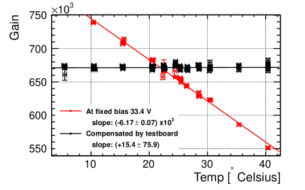
Figure 4 (right) shows the gain dependence on temperature for fixed bias voltage for SiPM CPTA 857. Again, we fit the data points with a first-order polynomial to extract the slope . Figure 5 (right) shows the dependence versus bias voltage. Again, we observe a linear dependence. A zeroth-order polynomial fit yields . Since this is in good agreement with the result of a first-oder polynomial fit, we use the result of the zeroth-order polynomial fit for the determination of . For most of the detectors studied, we see a linear dependence of versus V. From the and averages, we determine for SiPM CPTA 857. Since increases with and decreases with , the resulting values at high T and low V or low T and high V yield similar ratios leading to a uncertainty on . We define the uncertainty on the gain stability by
| (1) |
For SiPM CPTA 857, . Figure 6 (left) shows the measurements versus bias voltage for all 15 SiPMs tested. They fall into two groups. Hamamatsu MPPCs have values in the range and operate at higher bias voltage (65-75 V) while KETEK and CPTA SiPMs have values around operating at a bias voltage of and , respectively. Thus, we expect the gain stabilization to work better for KETEK and CPTA SiPMs than for Hamamatsu MPPCs.
5 Gain Stabilization
| Detector | G | ||||
|---|---|---|---|---|---|
| at | w board | w/o board | |||
| -5800 | |||||
| -14400 | |||||
| -38800 | |||||
| -3800 |
We have tested the gain stabilization method on four SiPMs including at least one SiPM from each manufacturer. We adjust the bias voltage continuously using the bias voltage regulator test board. We perform bias voltage readjustments for temperatures between and . At each temperature, we take 16 samples each with 50,000 waveforms. Figure 6 (right) shows the gain before and after stabilization versus temperature for the CPTA 857 sensor.
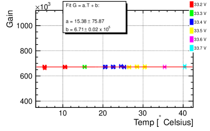
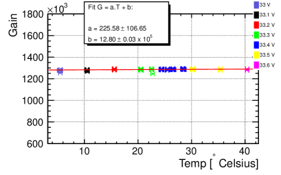
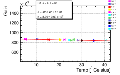
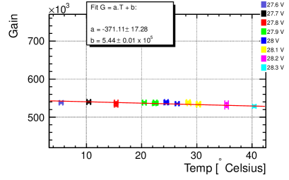
Figures 7 depict the results of the gain versus temperature dependence after bias voltage readjustment for SiPMs CPTA 857 (top left), CPTA 1677 (top right), KETEK W12 (bottom left) and Hamamatsu 11759 (bottom right), respectively. The color code indicates the range of the applied bias voltage, blue points correspond to the range . For SiPM CPTA 857, for example, we perform a linear fit to all data points and obtain an offset of and a slope of indicating that the fit is consistent with a uniform distribution. The deviation from constant gain in the entire temperature range extracted from a linear fit is . Table 2 shows the fit results of the gain after and before stabilization, and for all four SiPMs studied. Though the Hamamatsu MPPCs show the largest gain variation and largest , all tested SiPMs fulfill the requirements of having an uncertainty on the gain stability less than .
6 Determination of the dependence
Gain changes with respect to temperature and bias voltage variations are given by
| (2) |
In order to keep the gain constant, we set yielding
| (3) |
The ratio is obtained from a ratio of two first-order differential equations
| (4) |
for coefficients , and . For the linear case, the analytic solution for is simply
| (5) |
where is an integration constant. For , the solution is
| (6) |
If both and are constant, the solution is exactly linear
| (7) |
As an example, we have calculated the dependence for SiPM CPTA 857 assuming linear models for and . Figure 8 shows the resulting function . In the temperature range to , the function is well approximated by a first-order polynomial.

If and both have a quadratic dependence
| (8) |
with additional coefficients and , the analytic solution is of the form
| (9) |
where is again an integration constant and and represent
| (10) |
7 Conclusion and Outlook
We have tested 15 SiPMs from three manufacturers of which we selected four to show the performance of the gain stabilization. Hamamatsu MPPCs operate at a factor higher bias voltage than CPTA and KETEK SiPMs. The correction factor for the Hamamatsu MPPCs () is also about a factor of three higher than that for CPTA and KETEK SiPMs . In the full temperature range , the maximum voltage readjustments are less than for CPTA and KETEK (Hamamatsu) SiPMs. The deviation from constant gain, , after bias voltage readjustment is better than for CPTA, for KETEK and for Hamamatsu SiPMs. Since depends on , the deviation from constant gain is reduced by more than a factor of two if we limit the range to . For all four SiPMs, the uncertainty on the gain stability is less than in the full temperature range ( to ) as required. For constant, linear and quadratic and parameterizations, we determined analytical solutions for .
Since the results are encouraging, we have designed a bias voltage regulator board and ordered six prototype boards from an electronic company. We used one board in a recent stabilization test at CERN. We tested five SiPMs in the climate chamber extending the temperature range from to . We are presently analyzing the data to check if we need to make any modifications to the bias voltage regulator prototype and order if necessary new bias voltage regulator boards. Furthermore, we plan to implement our correction procedure into the the HBU of the front end electronics of the AHCAL technical prototype at DESY by modifying the power supply and demonstrate that the gain stabilization can be achieved.
ACKNOWLEDGEMENTS
We would like to thank Hamamatsu for providing samples of MPPCs with and pixel pitch and KETEK for providing SiPMs with pixel pitch. We further like to thank Lucie Linssen and Chris Joram for using their photon laboratory.
References
- [1] CALICE collaboration (C. Adloff , JINST 5, P05004 (2010).
- [2] G. Bondarenko el al., Nucl. Instrum. Meth. A 442, 187 (2000).
- [3] P. Buzhan el al., Proc. of the 7th Int. Conf. on Advance Technology Particle Physics, 717 (2002).
- [4] P. Buzhan el al., Nucl. Instrum. Meth. A 504, 48 (2003).
- [5] http://aida.web.cern.ch/aida/index.html
- [6] C. Soldner, PhD thesis, Ludwig Maximilian Universit at München (2013).
- [7] L. Weuste, PhD thesis, Ludwig Maximilian Universit at München (2013).
- [8] N. Dinu, Instrumentation on Silicon Detectors: from properties characterization to applications, LAL-13-192. Mémoire d’Habilitation, Université Paris-Sud 11, 2013.