Interplay of ferroelectricity and single electron tunneling
Abstract
We investigate the interplay of ferroelectricity and quantum electron transport at the nanoscale in the regime of Coulomb blockade. Ferroelectric polarization in this case is no longer the external parameter but should be self-consistently calculated along with electron hopping probabilities leading to new physical transport phenomena studying in this paper. These phenomena appear mostly due to effective screening of a grain electric field by ferroelectric environment rather than due to polarization dependent tunneling probabilities. At small bias voltages polarization can be switched by a single excess electron in the grain. In this case transport properties of SET exhibit the instability (memory effect).
pacs:
77.80.-e,72.80.Tm,77.84.LfSystems with ferroelectric (FE) elements attract much of attention due to their interesting fundamental properties at the nanoscale as well as due to their possible applications in microelectronics, especially in nonvolatile memory devices, in emerging technologies of Terahertz-detecting and in building of advanced (nano)capacitors. Dawber et al. (2003); Ahn et al. (2004); Dawber et al. (2005); Wang et al. (2007); Zhang et al. (2007); Scott (2007); Maksymovych et al. (2009a); Chu et al. (2008); Lee et al. (2008); Kalinin et al. (2010a); Sinsheimer et al. (2012); Callori et al. (2012); Ortega et al. (2012); Chanthbouala et al. (2012) In quantum junctions the ferroelectricity influences electron transport: Tunneling through the FE barriers shows giant electro-resistance effect caused by the strong dependence of electron tunneling probability on the FE polarization and external bias orientations. Maksymovych et al. (2009a); Zhuravlev et al. (2010) Here we focus on the inverse process — the influence of electron transport on ferroelectricity. Ahn et al. (2004); Kalinin et al. (2010a) The naive guess would be that a single electron, small quantum object, can slightly influence the macroscopic effect — ferroelectricity. However, we show that this is not quite true and discuss the interplay of ferroelectricity and quantum electron transport at the nanoscale in the regime of Coulomb blockade. Polarization in this case is no longer the external parameter but should be self-consistently calculated along with electron hopping probabilities leading to new physical transport phenomena studying in this paper. These phenomena appear mostly due to effective screening of a grain electric field by ferroelectric environment rather than due to polarization dependent tunneling probabilities.
Ferroelectrics (FE) are characterized by the polarization whose direction and magnitude can be changed by applying an external electric field larger than the ferroelectric switching field, . The ground ferroelectric state of a bulk sample is usually not uniformly polarized but divided into domains to lower the electrostatic energy, like in ferromagnets. Landau et al. (2004)

At the nanoscale to influence the polarization of (nano)ferroelectric one can apply strong enough bias to nanotips: Ahn et al. (2004) There is a well developed technique of imaging and control of domain structures in ferroelectric thin films by a tip of a scanning probe microscope, see, e.g., Refs. Gruverman et al., 1998; Ahn et al., 2004; Jesse et al., 2008; Rodriguez et al., 2009; Maksymovych et al., 2009a; Kalinin et al., 2010a.
Here we show how ferroelectric polarization switching can be produced by placing a single excess electron at the nanograin. Charged metal particle creates a strong enough electric field, MV/cm around it. Numerous ferroelectric (nano)materials have the same order of magnitude switching field. Ahn et al. (2004); Kalinin et al. (2010a)
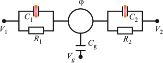
We study a single electron device with electric current flowing from the source to the drain electrodes with voltages and , respectively, Fig. 1. A metallic nanoparticle is placed in between these electrodes. The third gate-electrode controls the effective number of electrons on the grain through the capacitive coupling. We assume that the charging energy of a single grain is the leading energy scale in the problem, with being the temperature. The device shown in Fig. 1 is a standard Single Electron Transistor (SET) Averin and Likharev (1991); Averin et al. (1991); Devoret and Grabert (1992); Wasshuber (2001); Glatz et al. (2012); Chtchelkatchev et al. (2013a, b); Kafanov and Chtchelkatchev (2013) with one important exception: electrons tunnel through ferroelectric insulating layers.
The tunnel junctions between the nanograin and the electrodes form the capacitors with ferroelectric filling (see equivalent electric circuit Fig. 2). Typically, ferroelectric placed into the capacitor chooses polarization direction perpendicular to the electrodes. This configuration reduces electrostatic energy due to FE polarization screening by the electrodes. The direction of polarization can be switched applying the bias voltage to the capacitor. In SET the potentials of the electrodes and the gate potential are usually fixed. The grain potential can fluctuate and can be found by solving simultaneously the electrostatic and the electron transport problems. The potential depends not only on the bias voltage and capacitances, but also on the probability distribution to find electrons on the grain and on the polarization of ferroelectrics. Polarizations of ferroelectric layers in turn depend on the grain potential and . Thus we need to consider the self-consistent problem.
The solution of self-consistent problem strongly depends on the relaxation parameters of ferroelectric material: How quickly the polarizations can change (flip) during the characteristic time of charging(discharging) of SET by a single electron. Below we focus on two limiting cases when both ferroelectric layers have relaxation times much longer than one-electron charging-discharging time and vice-versa. These two cases correspond to qualitatively different behavior of FE SET.
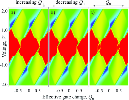
The case of slow FE is considered in Sec. I.2. We study the dependence of FE state on bias and gate voltages and show that the Coulomb diamonds have the “fine-structure” mediated by ferroelectricity that depends on the gate-voltage, Fig. 3 [at large enough ferroelectric polarizations this fine-structure can become comparable with the size of the diamonds]. We present the plot of FE “phase diagram”, Fig. 4. For large bias voltages polarization in both capacitors are co-directed and does not affect the electron transport. At small bias voltages the polarization can be switched by a single excess electron in the grain. In this case transport properties of SET exhibit the instability (hysteresis), Fig. 3. We emphasize that this instability appears even without the hysteresis of polarization .
In Sec. I.3 we discuss the case of fast FE. Then the instability is absent. However, we show that the Coulomb-Blockade peaks of zero-bias conductance as the function of the gate-voltage Averin and Likharev (1991); Averin et al. (1991); Devoret and Grabert (1992); Wasshuber (2001) become wider and finally disappear with increasing of the FE polarizations. Such an effect appears due to strong non-linear screening of electron charge in the grain by ferroelectrics leading to the suppression of the Coulomb Blockade. In Sec. II we discuss relation of our theory to real experimental situation.
I Single electron device with ferroelectric tunnel junctions
Below we discuss the basic properties of SET sketched in Fig. 1. The equivalent electric circuit is shown in Fig. 2. The ferroelectricity influences the properties of SET through two capacitors with FE insulating layers and results in the redistribution of charge over the surface of the nanoparticle. In particular, ferroelectric with polarization induces the local charge on the nanoparticle surface with the surface density , Landau et al. (2004) where is the normal to the surface. The excess charge on the nano-grain is given by the following expression
| (1) |
where is the number of excess charges, is the electron charge, is the potential of the nano-grain, with is the capacitance. The surface integration is performed over the nanoparticle sides playing the role of the capacitor plates in Fig. 2.
We study the SET with fixed electrodes and gate potentials and find the grain potential using Eq. (1). Following the “orthodox model” Averin and Likharev (1991); Averin et al. (1991); Devoret and Grabert (1992); Wasshuber (2001) we obtain the probabilities to find electrons on the grain. In the stationary case they satisfy the detailed balance equation
| (2) |
where the transition rate describes the change of grain charge from to electrons, see Appendix A. Calculating transition rates we neglect the dependence of electron tunneling amplitudes on the FE orientation, however this effect can be easy included in our consideration. Our estimates show that consideration of polarization dependent tunneling probabilities does not destroy the effect but it rather enhances it.
The electric current can be written in terms of the transition rates as follows
| (3) |
Here the upper index of refers to the particular tunnel junction, see Appendix A. Solving Eqs. (1)-(3) self-consistently we find the current .
The polarization of the FE is sensitive to the electric field and can be flipped by strong enough field. The characteristic time scale for electron tunneling is , with and being the total capacitance and the total resistance, respectively. The characteristic time scale for polarization change, , can be either larger or smaller than . Both cases are relevant for experiment and will be discussed below.
Here we consider the following model describing the electric field dependence of polarization Zhang et al. (2007); Yoon et al. (2003)
| (4) |
where being a material dependent parameter. Similar dependence of polarization on the capacitor voltage has the form , where and is the distance between the electrodes of the capacitor. Equation (4) describes the saturation of for large electric fields and it results in constant electric susceptibility for small electric fields, . Equation (4) neglects the spontaneous polarization and the hysteresis behavior of . This simplification is valid for FE with small switching field in comparison with the field created by the charged grain, Sec. II. Below we show that even in the absence of FE hysteresis the SET conductance has history dependence. To highlight this result we neglect the FE hysteresis in our consideration. The presence of memory effect in the behavior of polarization would add an additional hysteresis in the transport properties of SET.
I.1 Units for numerical calculations.
We use dimensionless units in our numerical calculations: is the unit of energy and temperature (). All charges are measured in units of elementary charge , in this units the electron has charge . The capacitance unit is , thus . We choose the bare tunnel resistance of the first tunnel junction, , between the left electrode and the nanograin for units of tunnel resistance, Figs. 1-2. Thus the unit of conductance is .
I.2 Mean-field approximation: Fast charging (discharging) and slow relaxation of polarization.
Here we consider the limit of fast grain charging and slow relaxation of polarization, . In this case the polarizations of the FE layers are defined by the average biases across the capacitors. The average grain potential is given by the following expression:
| (5) |
Below we show that and depend on the polarization of the FE layers that in turn depends on the average potential leading to the self-consistent problem.
We choose and for the biases applied to electrodes, solve Eq. (1) for the grain potential along with Eq. (4) and find
| (6) | |||
| (7) |
where , with and being the effective capacitance area. We notice that parameter is positive. Comparing Eq. (6) with the orthodox theory of SET Devoret and Grabert (1992); Wasshuber (2001) we find that the presence of ferroelectricity shifts the “gate charge” by the polarization-dependent constant, , see Appendix A.
We start our consideration with approximate solution of Eq. (5). When the current flows through the ferroelectric SET the induced FE charge stays the same. Therefore if we assume that the sum of the effective charges induced by the FE on the grain, is known we can calculate the probability distribution of electrons using the orthodox theory of SET. The only difference between the orthodox theory and our case is the presence of an additional shift in the parameter .
We assume the following: a) The induced FE charges are much smaller than the electron charge, and b) The bias voltage between the first and the second electrodes of the transistor is much smaller than the charging energy, . For and only zero or one excess electron can be found on the grain with appreciable probability which can be obtained using the orthodox theory, Appendix A.2
| (8) |
For simplicity we consider the case , , and where Eq. (8) has a trivial solution and two non-trivial solutions
| (9) |
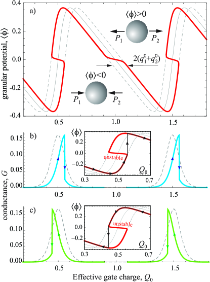
Equation (9) agrees well with numerical results in Fig. 5 for evolution of average grain potential vs. parameter . The graph is periodic in similar to the behavior of average grain potential of SET in the absence of FE. However, there are regions in Fig. 5 where parameter corresponds to multiple values of average potential . This behavior appears due to the reorientation of FE polarization by the average electric field inside the capacitors. Both FE orientations correspond to the same parameter . This ambiguity results in hysteresis behavior of the current.
The number of solutions in Eq. (8) depends on the system parameters , , and . The hysteresis loop shown in Fig. 5 corresponds to the case of three solutions in Eq. (8). The criterion for hysteresis is the following, see Appendix A.3:
| (10) |
The width of the hysteresis loop is given by the following expression
| (11) |
Fig. 6 shows the change of conductance hysteresis with voltage . It follows that conductance discontinuity generating the hysteresis decreases with increasing voltage and completely disappears above a certain critical value of , see, e.g., Eq. (10). This result is natural since increasing voltage produces larger FE polarizations leading to a more difficult re-polarization by the external field.
The hysteresis loop is still present even if the step-like dependence of in Eq. (8) is substituted by the linear relation .
Equation (10) can be written using the dielectric susceptibility of the proper dielectric as follows . Thus, any dielectric with static susceptibility satisfying the above criterion and with the characteristic reaction time exceeding time will produce the hysteresis behavior in the conductivity of SET. The hysteresis in this model appears due to slow FE (or dielectric). Then the FE feels only the average grain potential. We estimate parameters , , and the right hand side of Eq. 10 in Sec. II.
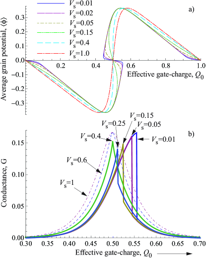
The zero voltage conductance of ferroelectric SET vs. is shown in Figs. 5(b)-(c). It is periodic in parameter similar to the SET without ferroelectricity. However, the presence of ferroelectricity breaks the reflection symmetry of conductance peaks and the peaks shape depends on the direction of change, see arrows in Fig. 5(b)-(c). Therefore there is a hysteresis in the conductance behavior similar to the branching theory, Vainberg and Trenogin (1974) where the points with trigger the jumps between the different branches of hysteresis loop.
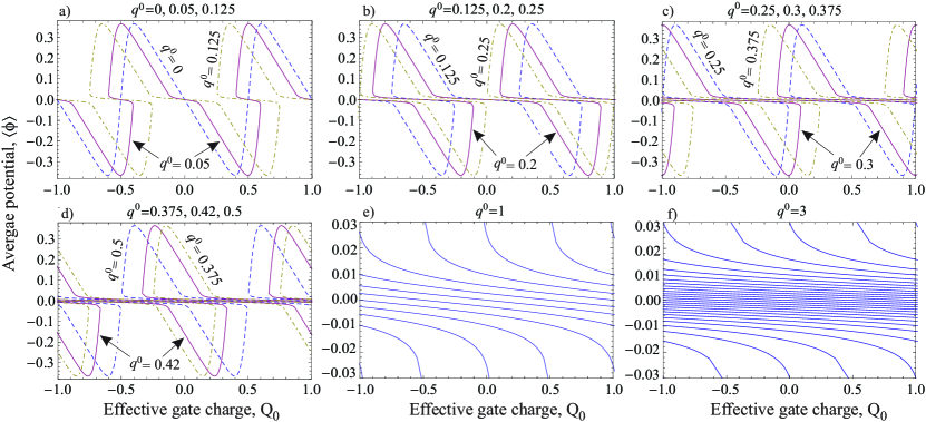
Similar hysteresis behavior shows the conductance density plot in Figs. 3 with Coulomb Diamonds, where Fig. 3(a) and (b) were obtained with forward and backward change of parameter , while Fig. 3(c) was obtained for forward-backward evolution of parameter . Ferroelectricity deforms the Coulomb diamonds: Near the half integer the Coulomb diamonds acquire the fine structure. However at large enough ferroelectric polarizations this fine-structure can become comparable with the size of the diamonds: The fine-structure characteristic size in the direction of is , for .
The hysteresis can be better understood using the energy balance consideration. The effective free energy of SET with excess charges on the grain for zero temperature and bias voltage has the form
| (12) |
Below we use dimensionless units discussing Eq. (12). First, we compare the energies of the system for . In this case for average grain potential according to Fig. 5 three choices are possible: and , where . The first choice corresponds to while two other choices to . The solution with corresponds to . [This value corresponds to the crossing point, , of two parabolas, , as functions of .] For two other cases the free energy, , is smaller by . Here we choose , thus the minimum in Eq. (12) corresponds to or . The solution is physically unstable at since it has the largest free energy. Similar consideration can be used in explaining the jumps between different branches of in Figs. 5(b)-(c).
Figure 5 shows that at zero voltage one can drive the system between two states with FE layers polarized toward or backward directions with respect the grain by changing parameter . This behaviour can be understood as follows: At zero bias voltage there is no preferable direction in the SET. Contrary, a finite bias voltage results in electric field which breaks the symmetry of the problem leading to two FE polarizations in parallel.
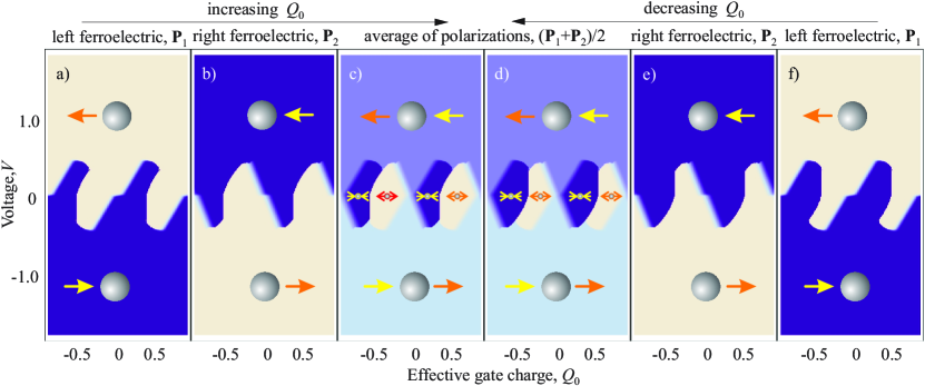
We confirm this presenting numerical calculations of FE polarizations in the -plane, Fig. 4, where the color gradients and the arrows indicate the polarizations of the left and the right ferroelectrics. Plots (a) and (b) show FE polarizations for increasing parameter [similar to Figs. 3a and 5b] while plots (e) and (f) show this polarization for decreasing [similar to Figs. 3b and 5c]. In fact, these graphs show the charges in the grain that screen the FE polarization. Graphs (c) and (d) show the arithmetical mean of the polarizations corresponding to the left and to the right ferroelectrics. To distinguish the non-zero total screening charge in the parallel case we choose parameters in Fig. 4 slightly different from Figs. 3-5: and .
Figure 7 shows the evolution of average grain potential for . There are several branches in the behavior of depending on the ratio . The peaks correspond to the first branch. The nearly linear segments of with the maximum much smaller than the peak hight correspond to the second branch. Figure 7(a)-(c) shows that the peaks of are periodic over with the period of (). The shift of -peaks at relative to the case is . The terms with , enter the expression for potential similar to the shift-renormalization of parameter . Figure 7(a)-(d) and (e)-(f) show that the second branch of potential is strongly non-periodic.
I.3 Fast ferroelectric. Polarization follows charging-discharging events.
Now we consider the opposite case of fast polarization following the charging-discharging process, . In this limit the polarization depends on the instant electric field instead of the average electric field as it was discussed before. Here we replace in the orthodox theory by , Appendix A. With this replacement Eqs. (6)-(7) remain valid with substitution of potential instead of average potential in Eq. (6).
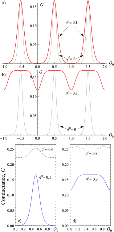
The conductance behavior is shown in Fig. 8. Ferroelectricity preserves periodicity over the parameter similar to the mean-field theory discussed in Sec. I.2. However, in this limit the hysteresis is absent while the broadening of the conductance peaks, Figs. 8(a)-(b), and the reduction of the peaks amplitude with increasing are present, Figs. 8(c)-(d).
In orthodox theory the conductance of SET in the absence of ferroelectricity and at low temperatures, follows the following relation
| (13) |
where is the deviation from the degeneracy point. The width of conductance peaks defines the temperature-parameter .
For FE the degeneracy points do not follow exactly the half integer . Above it was shown that FE polarization redefines where parameter depends on the polarization and the excess charge number . Therefore the conductance peak in Fig. 8(a)-(b) has the width and consists of many shifted conductance peaks (13). Thus the width of the peak-plato in Fig. 8b is approximately . Similar arguments explain the reduction of the conductance peaks amplitude with increasing parameter in Figs. 8(c)-(d).
The question about the average direction of polarizations can be investigated similar to the previous section. The results are similar, but in this case the hysteresis is absent.
II Discussion
II.1 Ferroelectric model
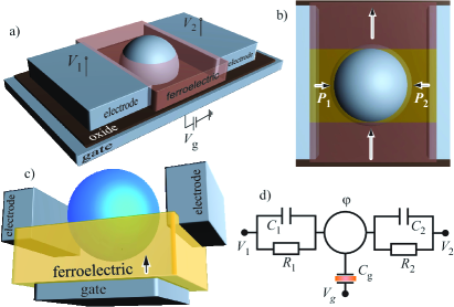
Ferroelecric SET consists of nanosized charged metallic grain embedded in a ferroelectric confined by the metallic leads, Fig. 9(a). The thickness of FE layer between the grain and the leads is few nm. It is known that even for such a thin FE film the continuum theories of ferroelectricity are valid. Ahn et al. (2004); De Guerville et al. (2005) To determine the state of FE under the influence of the charged grain one needs to solve the inhomogeneous Landau-Ginzburg-Devonshire (LGD) equation. Strukov and Levanyuk (1998) This question appears frequently in problems dealing with local modification of FE properties by the tip of scanning probe microscope. Kalinin et al. (2010b) We assume that domain wall thickness in FE is less than the grain size, . Kalinin et al. (2010b); Maksymovych et al. (2009b) The grain influences only the FE region between its surface and the leads, Fig. 9(b). Inside this region polarization is homogeneous and depends on the grain state. Outside this region the FE state does not depend on the grain charge. The side regions do not affect the electron transport. Udalov et al. (2014) With these assumptions the homogeneous LGD theory is valid for the description of FE behavior.
The FE material can be placed not only between the grain and the leads but also between the grain and the gate electrode, Figs. 9(c)-(d). In this case the FE layer does not have any metallic inclusion and can be made as a rather thick film. Such a geometry is relevant for experiment and allows to avoid problems with the influence of grain shape on the FE polarization. The transport equations for such SET are similar to the transport equation written above. For example, in Eq. (7) one should use , with being related to the FE between the gate and the grain.
The memory effect (hysteresis) in ferroelectric SET can be used for computer memory-cell with the measurement of the zero-bias conductance being the reading operation while the application of the gate voltage being the writing operation. Such a memory-cell will be discussed in the forthcoming publication.
II.2 Evaluation of parameters
In this section we discuss important physical parameters of FE SET such as FE and SET time scales, electric field due to metallic grain, the FE switching field, and the FE saturation polarization. These parameters define the physical behavior of FE SET.
In the previous sections we discuss two limits: i) slow () and ii) fast () ferroelectric. Estimates show that the characteristic time varies in a rather large range from dozens of nano- to picoseconds. This time is controlled by the system geometry and materials. The distance between the grain and the leads controls the resistivity of the SET, , the dielectric properties of the FE material, and the capacitance of the SET, . The FE switching time depends on the material and can be in the range of s Joshi and Krupanidhi (1993) to few nanoseconds. Larsen et al. (1991) Therefore both limits are relevant for experiment. SET with changing energy K have small capacitance, F leading to .
Discussing two limits we neglect the hysteresis loop of FE material (and thus, the spontaneous polarization). This assumption is valid for large electric field created by a single electron in a grain in comparison with the FE switching field, . This is typical for number of FE including Li-doped ZnO, Wang et al. (2003) Pb(In1/2Nb1/2)1-xTixO3, Tu et al. (2007) (PbMg1/3Nb2/3O3)x(PbTi)3)1-x, Tu et al. (2002) PZT, Hu and Krupanidhi (1993) and etc. The presence of hysteresis loop leads to more complicate picture of electron transport in FE SET with the interplay of FE hysteresis loop and the hysteresis appearing due to the interaction of FE with the grain, Sec. I.2. In the opposite limit, , the polarization becomes an external parameter as in the ordinary FE tunnel junctions.
The magnitude of FE saturation polarization strongly affects the electron transport for fast ferroelectrics, . If induced charge due to FE exceeds one electron charge the Coulomb blockade is suppressed leading to the conductivity independent of gate voltage. In this case the FE completely screens the electric field of an electron on the grain. To observe the conductivity peaks in Fig. 8 the FE environment should generate the charge smaller than one electron, (). Typical ferroelectrics, such as P(VDF-TrFE), PZT, (PbMg1/3Nb2/3O3)x(PbTi)3)1-x, have bulk polarization about e/nm2 leading to , for a few nm size grain. However, decreasing the thickness of FE film reduces its polarization. Fridkin (2006) For example, drastic polarization reduction from 1.5 e/nm to 0 e/nm is predicted for BaTiO3 when the thickness of the BaTiO3 film decreases from 15 nm to 3 nm. Junquera and Ghosez (2003) Suppressing of polarization with decreasing of FE thickness was observed in P(VDF-TrFE) films. Zhang et al. (2001)
For slow FE, Eq. 10 separates two regimes of FE SET with finite and zero hysteresis conductivity voltage dependencies. For estimates we write voltage using FE switching field, and the charge [we drop index ] using the FE polarization, . For e/nm, Wang et al. (2003) nm, nm, and temperature K we find the criterion for the appearance of hysteresis, MV/cm. This criterion is valid for almost all ferroelectrics. In addition, we note that in the case of slow FE the condition () results in simple hysteresis behavior of the system, its violation makes the behavior more complicated, but does not affect the existence of hysteresis.
III Conclusion
We investigated the electron transport in single-electron-device with ferroelectric active layers. We showed that there is an interplay of ferroelectricity and single-electron tunneling. We distinguish two different cases of slow and fast ferroelectric. In the first case the gate voltage dependent conductance shows the instability related to the spontaneous polarization inversion of ferroelectric polarizations. We show that similar instability may show also SET with slow dielectric. At small bias voltages the polarization can be switched by a single excess electron in the grain. In the case of fast ferroelectric instability is absent. However, we show that the Coulomb-Blockade peaks of zero-bias conductance as the function of the gate-voltage become wider and finally disappear with increasing of the FE polarizations. Such an effect appears due to strong non-linear screening of electron charge in the grain by ferroelectrics leading to the suppression of the Coulomb Blockade. Finally we show that our results could be observed experimentally.
IV Acknowledgments
N. C. was partly supported by RFBR No. 13-02-00579, the Grant of President of Russian Federation for support of Leading Scientific Schools, RAS presidium and Russian Federal Government programs. I. B. was supported by NSF under Cooperative Agreement Award EEC-1160504, NSF Award DMR-1158666, and NSF PREM Award..
Appendix A Orthodox theory of Ferroelectric Single Electron Transistor
A.1 Main equations
Below we outline the main steps that help to understand our results in the presence of ferroelectricity using the language of orthodox theory
In orthodox theory the rate describing the change of grain charge from to electrons through the first tunnel barrier, the left one in Fig. 2a), is
| (14) |
where is the Bose-function and is the tunnelling bare resistance. Similar expression can be written for the discharge process through the second tunnel barrier by changing the index “1” to “2”. Here is the change of effective free energy between the initial and the final states
| (15a) | ||||
| (15b) | ||||
where
| (16) |
In the orthodox theory, . For “slow” ferroelectric we have , while for “fast” we find . The –rates in the detailed-balance relations 2 are defined as follows
| (17a) | ||||
| (17b) | ||||
A.2 Approximation near the “degeneracy point”
The probabilities near the degeneracy point can be found using the orthodox theory
| (18) |
A.3 Hysteresis width
The criterion for conductivity hysteresis in Eq. 10 can be derived using Eq. 8 for average potential. This equation has three solutions if the slope, derivative of , of the function in the right hand side is larger than the slope of the linear dependence in the left hand side.
The estimate of the hysteresis width, , can be done using the following assumptions: 1) the polarization is linearly depend on the average potential ; 2) we replace the hyperbolic tangents by the piecewise straight function, if and if ; and 3) we neglect the “slow” function in the right hand side.
For the criterion of the conductivity hysteresis, Eq. 10, can be obtained using the formula for hysteresis width considering .
References
- Dawber et al. (2003) M. Dawber, I. Szafraniak, M. Alexe, and J. Scott, J. Phys. C 15, L667 (2003).
- Ahn et al. (2004) C. Ahn, K. Rabe, and J.-M. Triscone, Science 303, 488 (2004).
- Dawber et al. (2005) M. Dawber, K. M. Rabe, and J. F. Scott, Rev. Mod. Phys. 77, 1083 (2005).
- Wang et al. (2007) L. Wang, J. Yu, Y. Wang, G. Peng, F. Liu, and J. Gao, J. of Appl. Phys. 101, 104505 (2007).
- Zhang et al. (2007) Y.-J. Zhang, T.-L. Ren, and L.-T. Liu, Integrated Ferroelectrics 95, 199 (2007).
- Scott (2007) J. F. Scott, Science 315, 954 (2007).
- Maksymovych et al. (2009a) P. Maksymovych, S. Jesse, P. Yu, R. Ramesh, A. P. Baddorf, and S. V. Kalinin, Science 324, 1421 (2009a).
- Chu et al. (2008) Y.-H. Chu, L. W. Martin, M. B. Holcomb, M. Gajek, S.-J. Han, Q. He, N. Balke, C.-H. Yang, D. Lee, W. Hu, Q. Zhan, P.-L. Yang, A. Fraile-Rodriguez, A. Scholl, S. X. Wang, and R. Ramesh, Nature Materials 7, 478 (2008).
- Lee et al. (2008) W. Lee, H. Han, A. Lotnyk, M. A. Schubert, S. Senz, M. Alexe, D. Hesse, S. Baik, and U. Gösele, Nature Nanotechnology 3, 402 (2008).
- Kalinin et al. (2010a) S. V. Kalinin, A. N. Morozovska, L. Q. Chen, and B. J. Rodriguez, Rep. Prog. Phys. 73, 056502 (2010a).
- Sinsheimer et al. (2012) J. Sinsheimer, S. J. Callori, B. Bein, Y. Benkara, J. Daley, J. Coraor, D. Su, P. W. Stephens, and M. Dawber, Phys. Rev. Lett. 109, 167601 (2012).
- Callori et al. (2012) S. J. Callori, J. Gabel, D. Su, J. Sinsheimer, M. V. Fernandez-Serra, and M. Dawber, Phys. Rev. Lett. 109, 067601 (2012).
- Ortega et al. (2012) N. Ortega, A. Kumar, J. Scott, D. B. Chrisey, M. Tomazawa, S. Kumari, D. Diestra, and R. Katiyar, J. Phys. C 24, 445901 (2012).
- Chanthbouala et al. (2012) A. Chanthbouala, V. Garcia, R. O. Cherifi, K. Bouzehouane, S. Fusil, X. Moya, S. Xavier, H. Yamada, C. Deranlot, N. D. Mathur, M. Bibes, A. Barthélémy, and J. Grollier, Nature Materials 11, 860 (2012).
- Zhuravlev et al. (2010) M. Y. Zhuravlev, S. Maekawa, and E. Y. Tsymbal, Phys. Rev. B 81, 104419 (2010).
- Landau et al. (2004) L. Landau, E. Lifshitz, and L. Pitaevskii, Electrodynamics of continuous media, Vol. 8 (Elsevier Oxford, 2004).
- Gruverman et al. (1998) A. Gruverman, O. Auciello, and H. Tokumoto, Annu. Rev. Mater. Sci. 28, 101 (1998).
- Jesse et al. (2008) S. Jesse, P. Maksymovych, and S. V. Kalinin, Appl. Phys. Lett. 93, 112903 (2008).
- Rodriguez et al. (2009) B. Rodriguez, X. Gao, L. Liu, W. Lee, I. Naumov, A. Bratkovsky, D. Hesse, and M. Alexe, Nano lett. 9, 1127 (2009).
- Averin and Likharev (1991) D. Averin and K. Likharev, Mesoscopic phenomena in solids 30, 173 (1991).
- Averin et al. (1991) D. Averin, A. Korotkov, and K. Likharev, Phys. Rev. B 44, 6199 (1991).
- Devoret and Grabert (1992) M. Devoret and H. Grabert, Single Charge Tunneling, Vol. 264 (New York, Plenum, 1992).
- Wasshuber (2001) C. Wasshuber, Computational single-electronics (Springer, 2001).
- Glatz et al. (2012) A. Glatz, N. M. Chtchelkatchev, and I. S. Beloborodov, Phys. Rev. B 86, 045440 (2012).
- Chtchelkatchev et al. (2013a) N. M. Chtchelkatchev, A. Glatz, and I. S. Beloborodov, J. Phys. C 25, 185301 (2013a).
- Chtchelkatchev et al. (2013b) N. M. Chtchelkatchev, A. Glatz, and I. S. Beloborodov, Phys. Rev. B 88, 125130 (2013b).
- Kafanov and Chtchelkatchev (2013) S. Kafanov and N. M. Chtchelkatchev, J. Appl. Phys. 114, 073907 (2013).
- Yoon et al. (2003) Y.-K. Yoon, D. Kim, M. G. Allen, J. S. Kenney, and A. T. Hunt, Microwave Theory and Techniques, IEEE Transactions on 51, 2568 (2003).
- Vainberg and Trenogin (1974) M. Vainberg and V. Trenogin, Theory of branching of solutions of non-linear equations (Groningen: Wolters-Noordhoff B. V, 1974).
- De Guerville et al. (2005) F. De Guerville, I. Luk’yanchuk, L. Lahoche, and M. El Marssi, Materials Science and Engineering: B 120, 16 (2005).
- Strukov and Levanyuk (1998) B. A. Strukov and A. P. Levanyuk, Ferroelectric Phenomena in Crystals (Springer, Geidelberg, 1998).
- Kalinin et al. (2010b) S. V. Kalinin, A. N. Morozovska, L. Q. Chen, and B. J. Rodriguez, Rep. Prog. Phys. 73, 056502 (2010b).
- Maksymovych et al. (2009b) P. Maksymovych, S. Jesse, P. Yu, R. Ramesh, A. P. Baddorf, and S. V. Kalinin, Science 324, 1421 (2009b).
- Udalov et al. (2014) O. G. Udalov, N. M. Chtchelkatchev, A. Glatz, and I. S. Beloborodov, Phys. Rev. B 89, 054203 (2014).
- Joshi and Krupanidhi (1993) P. C. Joshi and S. B. Krupanidhi, Appl. Phys. Lett. 62, 1928 (1993).
- Larsen et al. (1991) P. K. Larsen, G. L. M. Kampschoer, M. J. E. Ulenaers, G. A. C. M. Spierings, and R. Cuppens, Appl. Phys. Lett. 59, 611 (1991).
- Wang et al. (2003) X. S. Wang, Z. C. Wu, J. F. Webb, and Z. G. Liu, Appl. Phys. A 77, 561 (2003).
- Tu et al. (2007) C.-S. Tu, R. R. Chien, C.-M. Hung, V. H. Schmidt, F.-T. Wang, and C.-T. Tseng, Phys. Rev. B 75, 212101 (2007).
- Tu et al. (2002) C.-S. Tu, C.-L. Tsai, J.-S. Chen, and V. H. Schmidt, Phys. Rev. B 65, 104113 (2002).
- Hu and Krupanidhi (1993) H. Hu and S. B. Krupanidhi, J. Appl. Phys. 74, 3373 (1993).
- Fridkin (2006) V. M. Fridkin, Phys. Usp. 49, 193 (2006).
- Junquera and Ghosez (2003) J. Junquera and P. Ghosez, Nature 422, 506 (2003).
- Zhang et al. (2001) Q. Zhang, H. Xu, F. Fang, Z.-Y. Cheng, F. Xia, and H. You, J. Appl. Phys. 89, 2613 (2001).