Quantum transport in carbon nanotubes
Abstract
Carbon nanotubes are a versatile material in which many aspects of condensed matter physics come together. Recent discoveries have uncovered new phenomena that completely change our understanding of transport in these devices, especially the role of the spin and valley degrees of freedom. This review describes the modern understanding of transport through nanotube devices.
Unlike in conventional semiconductors, electrons in nanotubes have two angular momentum quantum numbers, arising from spin and valley freedom. We focus on the interplay between the two. The energy levels associated with each degree of freedom, and the spin-orbit coupling between them, are explained, together with their consequences for transport measurements through nanotube quantum dots. In double quantum dots, the combination of quantum numbers modifies the selection rules of Pauli blockade. This can be exploited to read out spin and valley qubits, and to measure the decay of these states through coupling to nuclear spins and phonons. A second unique property of carbon nanotubes is that the combination of valley freedom and electron-electron interactions in one dimension strongly modifies their transport behaviour. Interaction between electrons inside and outside a quantum dot is manifested in SU(4) Kondo behavior and level renormalization. Interaction within a dot leads to Wigner molecules and more complex correlated states.
This review takes an experimental perspective informed by recent advances in theory. As well as the well-understood overall picture, we also state clearly open questions for the field. These advances position nanotubes as a leading system for the study of spin and valley physics in one dimension where electronic disorder and hyperfine interaction can both be reduced to a low level.
I Introduction and motivation
Carbon nanotubes are exceptional materials in many different ways. They are mechanically ultra-strong, the surface is perfectly clean, electrons move ballistically, and they vibrate like guitar strings with record-breaking quality factors. Moreover, by zipping nanotubes open one obtains the other wonder material, graphene. Together with C60-buckyballs and diamond, these allotropes of carbon have a central position in nanotechnology. Many of their properties have been studied and reviewed in great detail (e.g. Saito et al., 1998).
Nanotube electronic transport properties have been studied since the mid-1990s, first in bulk and since 1997 using individual single-wall nanotubes Bockrath et al. (1997); Tans et al. (1997). Many of the basic transport properties were quickly discovered, including Coulomb blockade, Fabry-Perot interference, 1D electronic interactions, Kondo physics, spintronics effects, and induced superconductivity. These properties have all been comprehensively reviewed, with both theoretical (e.g. Charlier et al., 2007) and experimental focus (e.g. Biercuk et al., 2008, Schönenberger, 2006)111The early generation of nanotube experiments that established basic quantum dot behavior was reviewed in Yao et al. (2001); Nygård et al. (1999). Open devices and early attempts to analyse the quantum dot shell structure were described in Liang et al. (2005); Sapmaz et al. (2006a). Hybrid devices involving superconducting and ferromagnetic leads have been reviewed in de Franceschi et al. (2010) and Cottet et al. (2006) respectively, while aspects pertinent to one-dimensional wires were addressed in Deshpande et al. (2010). Coupled quantum dots were introduced in e.g. Biercuk et al. (2008); Schönenberger (2006) whereas only recent reviews introduce spin-orbit interaction and valley physics Ilani and McEuen (2010); Kuemmeth et al. (2010), which are the themes of this review.. The general understanding in 2008 can be described as ‘consistent on a coarse scale’. On a fine scale the specific properties arising from residual disorder together with the specific, usually unknown, chirality of the nanotube under study were hampering a detailed description. On a coarse scale all nanotubes showed similar transport behaviour, but on a fine scale each experimentally studied nanotube was unique.
An important technical advance was a device scheme in which the nanotube was not exposed to any fabrication chemicals, thereby retaining pristine material quality Cao et al. (2005). Transport experiments on such “ultra-clean” nanotubes immediately showed more reproducible detail despite the still unknown chirality. Most importantly, the role of spin-orbit interaction was strikingly uncovered Kuemmeth et al. (2008). Although this spin-orbit interaction had already been predicted Ando (2000), it went unobserved and was therefore largely ignored until 2008. The experimental clarity revealed, however, that detailed understanding of quantum phenomena in carbon nanotubes has to include this effect.
The electronic orbits in nanotubes come in two flavors, known as the and valleys, that roughly correspond to clockwise and counterclockwise motion around the nanotube. The resulting quantum states form interesting superpositions of spin up and spin down with the and valleys. Our central aim is to present a coherent description of spin-orbit and physics in carbon nanotubes. We present the theory on a conceptual level and make references to detailed calculations in the literature. More details of the theoretical background are given in Appendix B. We highlight experimental results that demonstrate the essential concepts most clearly.
Spin-orbit and physics and their experimental consequences are first described in Secs. II-III for nanotubes confined as single quantum dots. The quantum dot geometry allows for a precise, straightforward description of energy eigenstates, which can be probed with well-established techniques of Coulomb blockade spectroscopy. Double quantum dots increase the complexity, with quantum states now described by three numbers: spin (up or down), valley ( or ) and location (left or right). Since the occupancy of both quantum dots is so easily controlled by gate voltages, the double dot geometry provides for exquisite experimental control. Section IV describes spin-valley selection rules for tunneling, probed by Pauli blockade experiments. The experimental control in double dots is utilized further in Sec. V describing the realization and operation of qubits employing various choice of basis states.
Sections II-V make use of a simplified model with electron-electron interactions included as a capacitive charging energy. In Sec. VI we extend this picture to include interactions between quantum dot states and the continuum in the leads. Quantum dots strongly coupled to leads show renormalization of the energy states as well as the formation of macroscopic coherence in a Kondo state. Sec. VI focuses on renormalization and Kondo effects in the specific context of spin-orbit and physics. In Sec. VII we consider interaction effects within quantum dots, which can be extraordinarily strong in the one-dimensional geometry of nanotubes. In quantum dots of a somewhat longer length, this leads to the formation of correlated Wigner molecules.
II Basics of carbon nanotube devices
II.1 Structure of carbon nanotubes
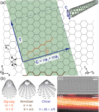
Carbon nanotubes consist of one or more concentric cylinders of graphene Saito et al. (1998). Both multi-wall and single-wall carbon nanotubes (MWCNTs and SWCNTs) can be synthesized and measured, but in this review, we will discuss only SWCNTs. As well as being simpler, these are the most studied both experimentally and theoretically.
The structure of nanotubes derives from the structure of graphene. A SWCNT is equivalent to a rolled-up strip taken from the two-dimensional honeycomb of carbon atoms that makes up a graphene sheet (Fig. 1(a)). Since there are infinitely many ways of selecting a strip to roll up, there are correspondingly many different nanotube structures. Each structure is specified by its chiral vector , which connects lattice sites on opposite sides of the strip that are superposed by rolling up into a nanotube. A given structure is labelled by its chiral indices , which are the coordinates of the chiral vector in terms of the graphene basis vectors . From Fig. 1(a), and are integers; to ensure that the same structure is not labelled two different ways, is conventionally taken in the range . Instead of specifying , a nanotube can also be described by its diameter and chiral angle , defined as the angle between and .
Two special cases are zig-zag structures () and armchair structures (), so called because of the arrangement of atoms along a cut normal to the nanotube. Structures not in either category are called chiral (Fig. 1(b)). Unlike armchair and zig-zag structures, chiral nanotubes lack inversion symmetry; the inversion isomer (with ) of an chiral structure is an structure. From the Onsager-Casimir relations, the transport properties of isomer pairs are expected to be similar, but they may differ in their nonlinear conductance in the presence of electron-electron interactions and time-reversal symmetry breaking by a magnetic field Ivchenko and Spivak (2002); Sanchez and Büttiker (2004); Spivak and Zyuzin (2004); Wei et al. (2005). The differences between isomer pairs, well established in optical measurements Samsonidze et al. (2004); Peng et al. (2007), are not discussed further here. Some structure parameters and their dependence on chiral indices are given in Table 1.
| Name | Symbol | Value |
|---|---|---|
| C-C bond length | 0.142 nm | |
| Graphene lattice constant | = 0.246 nm | |
| Graphene basis vectors | ||
| Graphene reciprocal lattice vectors | ||
| Graphene Dirac points | ||
| Chiral vector | ||
| ( integer; ; | ||
| ) | ||
| Chiral angle | ||
| Nanotube diameter |
This structure is confirmed by atomic-resolution microscopy. Transmission electron microscopy images the entire cross section, allowing exact chiral indices to be deduced (Fig. 1(c)). Nanotubes on surfaces can be imaged by scanning tunneling microscopy (Fig. 1(d)), although because of the poor edge resolution, the precise chirality is usually undetermined. Both images confirm the atomic arrangement of Fig. 1(a), with the same atomic spacing nm as graphite.
Unfortunately, high-resolution microscopy is usually incompatible with transport measurements and the chiral indices of nanotubes in electronic devices are often unknown. A few experiments have combined transport measurements with structure determination by electron diffraction Kociak et al. (2002); Allen et al. (2011). The structure can also be determined using optical Raman or Rayleigh spectroscopy, which is less invasive but does not always give unambiguous chiral indices Cao et al. (2004); Huang et al. (2005); Deshpande et al. (2009). Most of the results in this review will therefore be from nanotubes of unknown chirality; however, as discussed in the next section, the electronic properties of nanotubes are sufficiently independent of the chiral indices that most of the underlying physics can still be explored.
II.2 Quantum dots
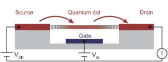
A basic carbon nanotube electronic device is shown in Fig. 2. The purpose is to allow measurement of the electrical current through a single nanotube Bockrath et al. (1997); Tans et al. (1997). To achieve this, the nanotube is contacted with metallic source and drain electrodes connected to an external circuit. A third electrode, the gate, coupled capacitively, allows the electrostatic potential to be tuned. Quantum dots are usually measured at low temperature ( K) to suppress thermal smearing of transport features.
A nanotube naturally confines electrons to one dimension. In quantum transport experiments, it is common to add longitudinal confinement by introducing tunnel barriers. These barriers can be created by modifying the electrostatic potential using gate voltages, often taking advantage of Schottky barriers induced near the metal contacts in the nanotube Heinze et al. (2002); Biercuk et al. (2008). The stretch of nanotube between the barriers where electrons are trapped is called a quantum dot. By studying the current through such a quantum dot as a function of bias, gate voltage, and other parameters such as magnetic field, the energy levels of electrons in the nanotube can be deduced. Quantum dot transport spectroscopy has been extensively reviewed e.g. in Kouwenhoven et al. (1997, 2001); Hanson et al. (2007). Basic concepts needed in this Review are explained in Appendix A.
II.3 Fabrication challenges of gated quantum devices
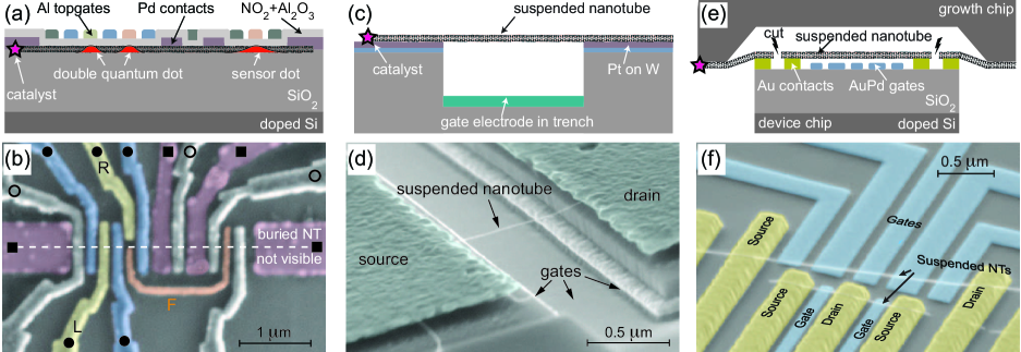
The realization of clean and tunable quantum dots in carbon nanotubes is not straightforward. Unlike carriers in III-V heterostructures, which are separated from the crystal’s surface by an atomically clean buffer layer, the nanotube’s -band is composed of atomic -orbitals that stick out perpendicular to the surface (see Sec. III). Patterning of gate oxides, mechanical deformation, and contamination from fabrication chemicals can easily induce disorder and irreproducible device characteristics Bezryadin et al. (1998); Zhu et al. (2005).
The characteristics of nanotube quantum dots depend on the bandgap, which varies widely between different nanotubes (Sec. III.2). Semiconducting nanotubes (bandgap eV) often show poor transport characteristics at low carrier density and low temperature. Presumably, this arises from unintentional localization of carriers into disordered puddles, facilitated by the carriers’ relatively large effective mass. Conversely, in quasi-metallic nanotubes (bandgap meV), controlled creation of sufficiently opaque barriers by electrostatic potentials is difficult, presumably due to the small effective mass (Sec. III.2.1). Kinks made by atomic force microscope (AFM) manipulation or mechanical templating can be used to locally induce bandgaps and backscattering centers Yao et al. (1999); Bozovic et al. (2001); Postma et al. (2001); Park et al. (2002); Biercuk et al. (2004); Stokes and Khondaker (2008), resulting in addressable tunnel barriers and Coulomb blockade even at room temperature. A similar effect can occur unintentionally due to disordered mechanical deformations induced by fabrication Bezryadin et al. (1998).
The largest experimental interest has been attracted by devices between these extremes (narrow-gap nanotubes). Tuneable tunnel barriers can then be induced rather easily by electrostatic gates. These nanotubes allow gate-controlled devices that do not uncontrollably break up into disordered puddles, yet their tunnel barriers remain tuneable over a wide range, even in the few-charge regime. Most devices can be classified according to whether gate fabrication occurs after nanotube growth (top gating), before growth (bottom gating), or on a separate chip (mechanical transfer method).
II.3.1 Top gating
The simplest way to make devices is usually to fabricate electrodes on top of nanotubes. This allows complex devices with many kinds of contact material including normal metals, ferromagnets, and superconductors. After growth or deposition, suitable nanotubes are imaged, and the electrodes are patterned by electron-beam lithography and liftoff. Early single-electron transistors were contacted in this way Bockrath et al. (1997), as were the first double quantum dots Mason et al. (2004). Although cleanliness and fabrication-induced disorder are a concern, devices fabricated this way have demonstrated ambipolar operation and discrete excited states Biercuk et al. (2005), as well as charge sensing and pulsed gate spectroscopy Biercuk et al. (2006); Gotz et al. (2008).
Full control of a double quantum dot requires at least five gate electrodes, necessitating thin, high-dielectric constant gate oxides (e.g. atomic-layer-deposited aluminum or hafnium oxide) and densely packed gate arrays Churchill et al. (2009b, a). Such a device is shown in Fig. 3(a,b), consisting of a fully tunable double quantum dot capacitively coupled via a floating gate to a charge-sensing single quantum dot on the same nanotube. Among other applications, these devices allow measurement of spin relaxation and dephasing (Sec. V). By selectively etching beneath the nanotube, suspended devices can also be fabricated Leturcq et al. (2009).
II.3.2 Bottom gating
A drawback of top gating is that the fabrication process itself can introduce disorder in the nanotube. An alternative is to grow or deposit nanotubes over predefined electrodes, resulting in devices with improved control and cleanliness Cao et al. (2005). Early single quantum dots were realized by depositing nanotubes across Pt source and drain electrodes, using the Si/SiO2 substrate as a backgate Tans et al. (1997). Similar to graphene devices, where suspending the layer dramatically improved the mobility Bolotin et al. (2008); Du et al. (2008), suspended nanotubes often show near-ideal transport characteristics, indicating that much of the disorder arises from interactions with the substrate Steele et al. (2009b); Ilani and McEuen (2010); Jung et al. (2013).
Motivated by the results of suspended single quantum dots as in Fig. 3(d), more complex contact and gate arrays were developed that can be loaded into the nanotube growth furnace as the last step before cool down and measurements Kuemmeth et al. (2008); Steele et al. (2009b). Although these devices were of high quality222Nanotubes that have never been in contact with solvents, resists, or a substrate are sometimes called “ultraclean” Deshpande et al. (2009); Steele et al. (2009b); Pei et al. (2012); Pecker et al. (2013); Waissman et al. (2013); Benyamini et al. (2014). and resulted in new discoveries, the harsh conditions in the growth reactor greatly restrict the materials and design. The overall device yield is low because a nanotube must grow across contacts and gates by chance.
II.3.3 Mechanical transfer
Mechanical transfer attempts to benefit from the best of both approaches, achieving high gate tunability without post-growth processing. The device chip (without nanotubes) and the growth chip (with nanotubes suspended across trenches) are fabricated separately. Just before measurement, a single nanotube is transferred from growth chip to device chip using an aligned stamping process Wu et al. (2010); Pei et al. (2012). By employing piezo-controlled scanning probe microscope manipulators, the transfer is possible in vacuum at cryogenic temperatures Waissman et al. (2013), allowing the cleanliness of the nanotube to be tested in situ. A state-of-the-art example is shown in Fig. 3(e-f).
II.4 Nanotube synthesis and isotopic engineering
For research applications nanotubes are readily synthesized in desktop furnaces, using chemical vapor deposition (usually from methane, ethanol or ethylene) in the presence of suitable catalysts Kong et al. (1999); Kuemmeth et al. (2010). Unlike III-V devices such as GaAs double dots, in which all stable isotopes possess a nuclear magnetic moment, carbon nanotubes allow fabrication of devices with and without nuclear spins in the host material in a straightforward way.
Nanotubes synthesized from natural hydrocarbons consist of 12C and 13C. By using isotopically purified 13CH4 or 12CH4, the isotopic composition can be tuned during growth. This not only affects the phonon modes (revealed by Raman spectroscopy Liu and Fan (2001)), but also the electron spin properties, because 13C possesses a nuclear spin , while 12C has . As discussed in Sec. IV.4, a local spin impurity (such as 13C) can flip the spin and/or valley of an electron.
III Carbon nanotube bandstructure
Just as the atomic structure of carbon nanotubes can be derived from that of graphene, the electronic band structure inherits from graphene many of its properties. However, the simple effect of being rolled up drastically modifies the band structure, leading to many effects that are not present in graphene. The most dramatic difference is the introduction of a bandgap, which allows electrons in nanotubes to be confined using gate voltages, but a variety of other subtle effects arise.
Briefly, the results are as follows. Although graphene is a semimetal, the formation of a nanotube leads to a confinement bandgap (a few hundred meV) for two-thirds of the possible structures. These are known as semiconducting nanotubes. Most of the remaining nominally metallic nanotubes show narrow bandgaps ( meV) due to a combination of curvature and strain. If the bandgap is undetectibly small, the nanotube is called quasimetallic, and a metallic nanotube is defined as one for which the bandgap is exactly zero. More subtle details of the band structure become evident in a magnetic field, including a magnetic moment associated with the valley degree of freedom, and spin-orbit coupling that is much stronger than in graphene and arises from curvature.
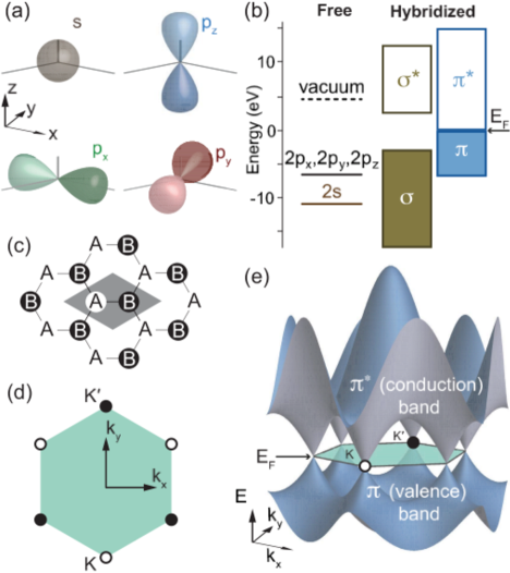
III.1 From atomic carbon to graphene band structure
To understand nanotube band structure, we begin with the energy levels of atomic carbon. In a free atom, the six electrons occupy the configuration . The outermost atomic shell includes one spherically symmetric -orbital and three -orbitals , , (Fig. 4(a)). Because of twofold spin degeneracy in each orbital, there are therefore eight states in the outermost shell of the atom, of which four are occupied.
The energy splitting is small enough (less than a typical bond energy) that all four outermost orbitals can hybridize to form covalent bonds. For a given structure, the number of orbitals that hybridize with the orbital is determined by symmetry. In graphene, the orbital, oriented perpendicular to the plane, is odd under inversion and therefore cannot hybridize with the even-parity orbital. No such symmetry protects the and orbitals. This type of hybridization, in which an -orbital is mixed with two -orbitals, is known as hybridization.
In graphene, these three orbitals further hybridize across neighbouring atoms in the crystal, forming a low-energy (bonding) band and a high-energy (antibonding) band (Fig. 4(b)). Likewise, hybridization of the orbitals forms bonding and antibonding bands denoted and , although with smaller bonding energy because the interatomic overlap is less. In undoped graphene, the electrons exactly fill the bonding bands, with three electrons per atom occupying and one occupying . The band remains filled at all times and does not participate in transport. The electrical behaviour of nanotubes is therefore determined almost entirely by the properties of the and bands.
Ignoring spin-orbit coupling, the orbitals do not hybridize with any of the lower-lying states, so the structure of the and bands follows simply from energy levels in the honeycomb graphene potential. Graphene consists of a rhombus unit cell with a two-atom basis (Fig. 4(c)), and has the hexagonal Brillouin zone shown in Fig. 4(d). The corners of this hexagon in -space are alternately labelled or . Because the three points are connected by reciprocal lattice vectors, by Bloch’s theorem they correspond to equivalent electron states; likewise, the three points are equivalent to each other, but not to the points. States close to the point are time-reversal conjugates of those close to the point.
The band structure that arises from this potential (Fig. 4(e)) has quite unusual properties Wallace (1947); Saito et al. (1998); Castro Neto et al. (2009). Although there is no bandgap, the and bands touch only at and , where the density of states is zero. Since the available electrons exactly fill the band, these points are where the Fermi level intersects the band structure, so that undoped graphene is neither a true metal nor a true semiconductor, but a semimetal. Close to the Fermi surface, the dispersion relation is linear, with a slope that determines the Fermi velocity333This value is derived from numerical simulations of graphite Painter and Ellis (1970); Tatar and Rabii (1982); Trickey et al. (1992) and nanotubes Mintmire et al. (1992), which indicate (although interactions may renormalize the value significantly Kane and Mele (2004)), as well as nanotube STM density-of-states measurements Wildoer et al. (1998); Odom et al. (1998) and ballistic electron resonance experiments Zhong et al. (2008), which give . . Expanding about the or point by writing or , and defining as the zero of energy, the dispersion relation for is simply
| (1) |
where the sign applies to electrons and the to holes. Because this dispersion relation also describes massless Dirac fermions, the points where the bands touch are known as Dirac points, and the nearby bands as Dirac cones. The correspondence of electron states in a nanotube with solutions of a Dirac-like equation is explained in Appendix B. Although we use this correspondence only in a few places in this Review, it is theoretically convenient because it allows many effects on nanotube band structure to be derived as perturbations to the Dirac equation.
III.2 Semiconducting, narrow-gap and metallic nanotubes
III.2.1 Theory: the zone-folding approximation
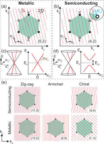
Since the nanotube diameter is usually much larger than the interatomic spacing, the graphene band structure is to a good approximation unperturbed by rolling up into a nanotube except for the imposition of a periodic boundary condition Hamada et al. (1992); Saito et al. (1992). This is known as the “zone-folding approximation”. The boundary condition to ensure single-valuedness is that , where is an integer, i.e. the component of perpendicular to the nanotube axis is . The allowed -values correspond to a series of lines in reciprocal space, known as quantization lines, running at an angle from the axis (Fig. 5(a-b)).
The one-dimensional dispersion relation is a cut along the quantization lines of the two-dimensional graphene dispersion relation. Since it is the branches closest to that determine transport properties, we neglect the other branches. The nanotube bandgap depends on the minimum separation of the quantization lines from the Dirac points. There are two possible situations. If quantization lines run straight through the Dirac points (Fig. 5(a,c)), then is linear near , giving zero bandgap and a metallic nanotube. However, if the lines bypass the Dirac points with separation , the situation is as shown in Fig. 5(b,d). The dispersion relation gives a pair of hyperbolae with bandgap , and therefore a semiconducting nanotube.
In the zone-folding approximation, the bandgap is determined by a simple rule: If is a multiple of three, the nanotube is nominally metallic Hamada et al. (1992); Saito et al. (1992). Otherwise, it is semiconducting, with bandgap . In a collection of nanotubes with random chiral indices, semiconducting nanotubes will therefore outnumber metallic ones by approximately 2:1. Figure 5(e) illustrates how the chiral indices determine whether the quantization lines intersect the Dirac points for various nanotube structures. Examples of both cases are shown for the three kinds of structure defined in Fig. 1(b), with one exception: Zig-zag and chiral tubes can be either semiconducting or metallic, but all armchair nanotubes are metallic.
The nanotube structure also sets the electron dispersion relation and hence the effective mass. The equation of the hyperbola in Fig. 5(d) is Zhou et al. (2005):
| (2) |
This low-energy dispersion relation is clearly electron-hole symmetric. This is a fragile symmetry, because any charge in the environment couples oppositely to electrons and holes, but it is sometimes reflected in data Jarillo-Herrero et al. (2004).
The effective mass arises from the curvature of the dispersion relation and for low energy () is:
| (3) |
where is the free electron mass. A bandgap of meV corresponds to effective mass , smaller than that in many conventional semiconductors (e.g. in GaAs ). Because small leads to larger longitudinal level spacing, nanotubes with small are often preferred for quantum dot experiments.
III.2.2 Valley as a robust quantum number
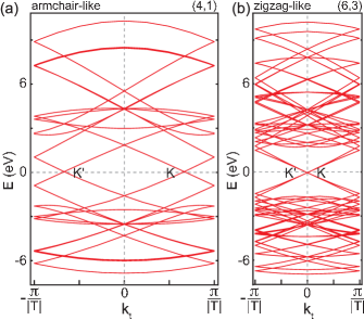
Just as in graphene, the band structure in nanotubes is characterized by the distinct and time-conjugate valleys and . In graphene the robustness of the valley quantum number is linked to the symmetries of the lattice. Mixing between valleys requires a large transfer of crystal momentum, and is therefore weak in a smoothly varying Coulomb potential. This is less obvious in metallic nanotubes, because the two Dirac points sometimes remain well separated in momentum space, and sometimes they merge at . In fact, all metallic nanotubes (see Fig. 6) can be divided into two classes Samsonidze et al. (2003); Marganska et al. (2014): the Dirac points are either well-separated in longitudinal momentum space (such nanotubes are known as armchair-like metals), or collapse to the origin of the longitudinal Brillouin zone (zigzag-like metals). For chiral metallic nanotubes, this classification is possible by introducing a helical translational basis vector Lunde et al. (2005). For the zigzag-like metals, the two bands at are distinct by having different crystal angular momentum Lunde et al. (2005), where the angular momentum is defined as the quantum number related to the rotation part of the helical symmetry White et al. (1993). In the armchair-like metals, the angular momenta are the same, but their longitudinal crystal momenta differ by . Consequently, in both cases valley-valley scattering is suppressed by a difference in crystal angular momenta or crystal longitudinal momenta. Scattering within a valley may also require atomically sharp Coulomb scatterers or lattice imperfections, due to the spinor structure of the solutions to the Dirac equation, which differs between right movers and left movers Ando and Nakanishi (1998); Ando et al. (1998); Roche et al. (2001); McEuen et al. (1999).
Armchair-like and zigzag-like band structures are exemplified in Fig. 6. The number of subbands equals the number of carbon atoms in the unit cell of the nanotube, spanned by and in Fig. 1(a). Each subband shown is two-fold degenerate due to spin, and arises from a mapping of the quantization lines in Fig. 5 into the 1D Brillouin zone of the nanotube.
The above discussion applies to narrow-gap nanotubes, i.e. those that would be metallic in the zone-folding approximation but where other perturbations introduce a small bandgap (Sec. III.3). For nanotubes that are semiconducting even in the zone-folding approximation White et al. (1993); Mintmire and White (1995), the situation is similar. This can again be seen using helical quantum numbers White et al. (1993); Mintmire and White (1995) as follows: All bands can be classified by their crystal angular momentum, which means that mixing of two bands with different crystal angular momentum is protected (as for zigzag-like metallic tubes). Mixing of bands with the same crystal angular momentum is suppressed by their difference in wavenumbers when folded onto the smaller translational Brillouin zone.
Local Coulomb scatterers can flip the valley index Pályi and Burkard (2010); Bercioux et al. (2011), and spin-carrying impurities can flip both spin and valley with comparable rates Pályi and Burkard (2009). One example is hyperfine coupling to nuclear 13C spins, which can cause both spin and valley relaxation (Sec. IV.4). Another example is the local part of the electron-electron interaction, discussed in Sec. VII and Appendix B. In addition, electrical contacts can induce valley scattering due to valley mixing during tunneling (Sec. VI.3).
III.2.3 Experiment
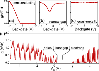
Nanotubes of different kinds can be distinguished experimentally by measuring the current as a function of at fixed , as in Fig. 7(a-c). The gate potential shifts the energy levels up or down and therefore tunes the position of the gap relative to . Tuning into the bandgap suppresses the current. This can be seen in Fig. 7(a), where the Fermi level is shifted from the valence band (for ) to the bandgap (for ), showing that the nanotube is semiconducting. A quasi-metallic nanotube, by contrast, is one with no dependence on (Fig. 7(c)), indicating , where is Boltzmann’s constant and is temperature.
Experimentally, the fraction of nanotubes showing quasi-metallic behavior at room temperature is very small () Cao et al. (2005); Churchill (2012). More common is ‘narrow-gap’ behavior (Fig. 7(b)), where partial current suppression indicates a small bandgap at room temperature Ouyang et al. (2001). This interpretation is confirmed by low-temperature experiments (Fig. 7(d)), where precise measurements from Coulomb peak positions frequently give meV (e.g. in Fig. 7(d), meV). To explain such small bandgaps from circumferential quantization alone requires nm, which might be structurally unstable and is excluded by AFM topography measurements. More likely, nearly all nanotubes that the zone-folding model predicts should be metallic acquire narrow bandgaps by perturbations discussed in the next section.
III.3 Structural origins of the narrow gap
III.3.1 Theory
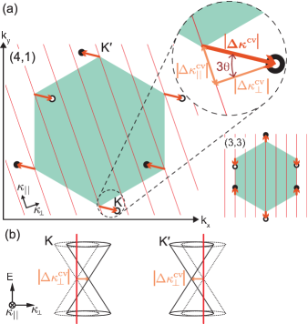
The zone-folding approximation assumes that the allowed electron states in nanotubes are exactly the same as their equivalents in graphene. Perturbations arise if the symmetry of the carbon bonds is broken by changing the overlap between adjacent electron orbitals. One unavoidable example is the curvature of the rolled-up sheet Blase et al. (1994). This has two effects on the band structure. First, it leads to a small renormalization of the Fermi velocity by at most a few percent, which is insignificant in experiments Izumida et al. (2009). More importantly, it displaces the Dirac points in reciprocal space away from and Kane and Mele (1997); Izumida et al. (2009), because it breaks the equivalence of the three bond directions. This shift is parameterized by a displacement vector (Fig. 8(a)), and is opposite for and because states in the two valleys are time-reversed conjugates of each other Castro Neto et al. (2009). In semiconducting nanotubes, is much smaller than the offset arising from quantization, and therefore has only a small effect. However, in nominally metallic nanotubes, the shift of the Dirac cones relative to the quantization lines introduces a bandgap , where is the component of perpendicular to the nanotube axis (Fig. 8(b)). (The component parallel to the axis, , has no effect.) This curvature-induced bandgap is always much smaller than the quantization energy difference. Unlike the quantization bandgap, it depends on the chiral angle. As shown in the inset of Fig. 8(a), the vector points at an angle of from the perpendicular. The curvature-induced bandgap is therefore proportional to ; it is calculated to be Kane and Mele (1997); Park et al. (1999); Yang et al. (1999); Yang and Han (2000); Kleiner and Eggert (2001); Izumida et al. (2009); Klinovaja et al. (2011a):
| (4) |
For armchair nanotubes (Fig. 1(b)) and therefore . These are the only nanotubes expected to be truly metallic, if no other perturbation is applied (see Appendix B for more theoretical details).
A gap of similar magnitude can be opened by strain, in a way that also depends on nanotube chirality Heyd et al. (1997); Kane and Mele (1997); Rochefort et al. (1998); Yang and Han (2000). A uniaxial strain has the same symmetry-breaking effect as curvature (namely to break ), and therefore leads to a Dirac point displacement in the same direction with magnitude
| (5) |
where is the Poisson ratio and is a parameter related to the carbon-carbon bond force constants Nisoli et al. (2007); Huang et al. (2008). A torsional strain displaces the Dirac points by an amount at an angle from the perpendicular Yang and Han (2000). The uniaxial bandgap is therefore proportional to , while the torsional bandgap is proportional to . A third type of strain, nanotube bending, has no first-order effect on the bandgap for any structure Kane and Mele (1997). Numerical estimates of these effects are given in Table 3.
III.3.2 Experiment
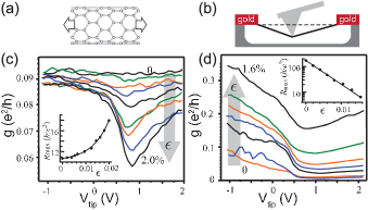
The existence of a narrow gap in nominally metallic nanotubes was first shown in density of states measurements by scanning tunneling microscopy Ouyang et al. (2001). For zig-zag nanotubes, a diameter dependence was found, in close agreement with theoretical expectations. Isolated armchair nanotubes showed no bandgap, consistent with the expected dependence (and implying negligible torsion for nanotubes lying on a surface). Many transport experiments have since found bandgaps of this order of magnitude, although usually without identifying the chirality.
In transport measurements, quasi-metallic nanotubes typically show bandgaps a few times larger than expected from curvature alone, suggesting a significant contribution from strain. The sensitivity of the bandgap to uniaxial strain has been measured by using an AFM tip to apply tension to suspended nanotubes Minot et al. (2003). By varying the applied force, it was possible both to induce a bandgap where none had been present before, and to decrease the bandgap in a semiconducting nanotube (Fig. 9). From the variation of conductance with strain, it was possible to deduce for the metallic and for the semiconducting nanotube, both with unknown chirality, where is expressed as a percentage elongation of the nanotube. Both values are comparable with that expected from Eq. (5), . Similar results, including confirmation of the dependence, have been obtained by optical methods Huang et al. (2008).
III.4 Longitudinal confinement and quantum dot energy shells
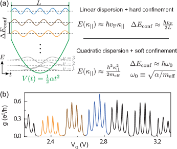
Different modes of the longitudinal wave function in a quantum dot of length lead to different confinement energies . The mode spectrum can be quite complicated, depending on the bandgap, boundary conditions, and interactions. The confinement can be classified as atomically sharp or non-sharp McCann and Fal’ko (2004), with the latter further subdivided into hard-wall or soft-wall cases depending whether the potential rises over a shorter or a longer distance than the dot length. An additional complication arises from the fact that bound states are formed from right and left moving Dirac particles that do not necessarily have the same group velocity in the unconfined nanotube. In Fig. 6 right-movers and left-movers within a valley travel at different speeds. This effect arises away from due to trigonal warping of flat graphene. If curvature of the nanotube is also taken into account (not shown in Fig. 6), an even stronger asymmetry arises. This happens already at and directly affects how standing waves are constructed. For example, if the confinement is sharp, then the discrete eigenstates of the quantum dot will be superpositions involving both valleys Izumida et al. (2012). We mention two simple limiting cases (Fig. 10(a)). Electrons (or holes) with low enough energy sample only the region near the potential minimum where confinement is parabolic (“soft-wall confinement”). If the energy is also much less than , so that by Eq. (3) the electron behaves as a massive particle (e.g. in a sufficiently large few-electron dot), the spectrum is harmonic with mode spacing , where is the harmonic frequency. Conversely, in a many electron-quantum dot the kinetic energy may both be large enough to reach the hard walls of the potential well and be in the linear part of the dispersion relation Eq. (2), so that the velocity is , independent of energy. The longitudinal modes then take on a sinusoidal form (Fig. 10(a)). The modes are again regularly spaced in energy, but now with Tans et al. (1997). This regular spacing, first observed by Liang et al. (2002), suggests that this picture is accurate in at least some real devices. If neither of these cases applies, or if the potential is strongly disordered, the mode spacing need not be regular. For example, when the electrons behave as massive particles in a hard-wall potential, the confinement energy is given by , with .
A set of states with the same mode index is called a shell. As explained in the next section, each state is characterized by twofold spin and valley quantum numbers, and thus the number of single-particle states per shell is four. In the so-called constant-interaction model (Appendix A), the quantum dot states are filled in order of increasing energy, so that contributes to the Coulomb peak spacing only for every fourth electron. This is evident in the ground-state spectroscopy data of Fig. 10(b). The regular shell spacing shows that single-particle energy levels, in combination with the constant-interaction model, are a good approximation.
III.5 Orbital magnetic moment
Because each state in the valley has a time-reversed conjugate in the valley, time-invariant perturbations such as curvature and strain do not break the degeneracy between them. This degeneracy can, however, be broken by a magnetic field. Intuitively, this can be seen by associating each state in the nanotube with a direction of circulation and hence a valley-dependent magnetic moment. This section shows how this orbital magnetic moment arises and is evident in the energy levels.
III.5.1 Theory
The orbital effect of a magnetic field on an electron with charge is captured by modifying the bare-electron Schrödinger equation so that the momentum operator is replaced by , where is the vector potential and Merzbacher (1998). So long as varies slowly on the scale of the lattice potential, the effect of this replacement on an electron confined in a closed loop is to add an Aharonov-Bohm phase to its eigenfunctions: if is an eigenstate at , then
| (6) |
is an eigenstate at finite with the same energy Luttinger (1951); Hofstadter (1976). In other words, the finite-field dispersion relation is related to the zero-field dispersion relation by:
| (7) |
Here the field induced shift is , with Ajiki and Ando (1993); Lu (1995)
| (8) |
where is the component of along the nanotube axis , the corresponding component of , and is the direction of the chiral vector. The quantization condition, however, is unchanged.
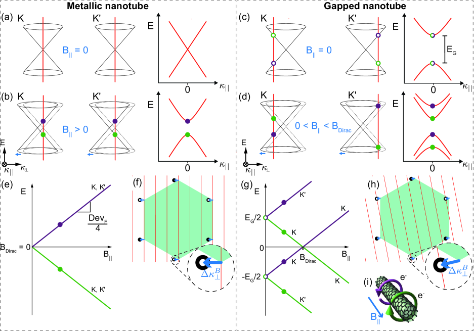
The consequences for the band structure are shown in Fig. 11. For a true metallic nanotube (Fig. 11(a-b)), the Dirac cones are shifted horizontally away from the quantization lines, opening a bandgap . If the nanotube already has a bandgap, the effect of the magnetic field is opposite for the two valleys (Fig. 11(c-d)). In one valley, the electron energy is initially reduced by ; in the other, it is increased by the same amount. At a field , one of the Dirac cones crosses a quantization line and the bandgap vanishes. Increasing beyond causes the bandgap to increase again. For a true semiconducting nanotube, can be as large as T and is usually outside the experimental range, but for quasi-metallic nanotubes can be just a few tesla. Because the effective mass depends on bandgap (Eq. 3), can be tuned by magnetic field.
The ground-state energies are plotted in Fig. 11(e-g) as a function of magnetic field. Each zero-field level is two-fold split, with slopes . This linear splitting allows each state to be assigned a magnetic moment , which has a straightforward physical interpretation (Fig. 11(i)): Electron states with positive (negative) magnetic moment correspond to clockwise (counterclockwise) circulation of electrons around the nanotube. In this interpretation, the direction of circulation for the first electron switches as the field is swept through . A similar picture applies in the valence band. The orbital moment is related to the band structure by:
| (9) |
where is the two-dimensional energy function describing the Dirac cone. For a low-energy electron (), this has the value:
| (10) |
To emphasize the analogy with Zeeman spin splitting, an orbital -factor is sometimes defined, where is the Bohr magneton. For a nanotube with a bandgap, the magnetic energy in a parallel field is then:
| (11) |
where is the spin -factor, the sign applies for electrons (holes), and the valley and spin quantum numbers are denoted by for and for , with the spin axis, along , being parallel to the nanotube444Our convention for assigning valley labels is that conduction-band states decreasing (increasing) in energy with increasing are labelled ..
III.5.2 Experiment

The orbital energy splitting can be seen in Coulomb ground-state spectroscopy as a function of magnetic field (Fig. 12), which shows the contribution to the single-particle energy levels Minot et al. (2004). Ignoring spin-orbit coupling (to be discussed in the next section), the first four electrons fill the four lowest states in order of energy: , , , . Subsequent electrons must enter a higher shell of the dot, but repeat the fourfold filling sequence for spin-valley states. The expected pattern of ground state energies is therefore alternating pairs with positive and negative magnetic moments. Typical data is shown in Fig. 12 for the first three hole shells. The measured magnetic moments, meV/T, are of the expected magnitude for orbital coupling with nm. In terms of orbital -factors, this would correspond to , much larger than , qualitatively confirming the picture in the previous section. For a quantitative comparison with theory, an independent measurement of is necessary. This was achieved using an AFM for a nanotube with nm, for which meV/T was measured, in fair agreement with the value meV/T expected from Eq. (10) Minot et al. (2004).
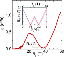
As seen from Fig. 11, a nanotube that is semiconducting at zero field becomes metallic in a parallel field with magnitude . This peculiar metal-semiconductor transition is specific to the cylindrical form of nanotubes and in fact recurs periodically with every flux quantum, that threads the cross section. For a semiconducting nanotube, the gap closes twice per period, at flux equal to and where the open and filled circles respectively in Fig. 11(h) cross quantization lines. The semiconducting gap reopens completely at . Figure 13 shows magnetoconductance of a semiconducting nanotube for which an AFM determined nm. For this diameter, the expected is 27 T, which is accessible at dedicated facilities. The nanotube has low conductance at zero field when is tuned into the gap. At 22 T the conductance is maximal, likely since the band gap is reduced to a smaller value. The band gap reopens to a maximum near 37 T before closing again as expected. The inset curve is calculated for nm and predicts gap minima at 27 T and 55 T. The observed conductance maximum, corresponding to the first gap closing, occurs at a somewhat lower field of 22 T, which is attributed to strain.
Equation (10) assumed an electron with zero longitudinal momentum. For electrons confined in a quantum dot, is reduced, for the following reason Jespersen et al. (2011a). As seen from the insets of Fig. 14, the partial derivative in Eq. (9) decreases with increasing ; the larger , the smaller the fraction of directed around the nanotube and hence the smaller . Because of confinement the shells participating in transport consist of superpositions of states with . (This can be seen for the sequence of shells in Fig. 10.) The total orbital moment therefore decreases with increasing confinement energy (Fig. 14), with predicted scaling Jespersen et al. (2011a):
| (12) |
where is the unconfined value derived from Eq.(10),
| (13) |
and is the bandgap at zero magnetic field without spin-orbit coupling. Figure 14 shows a series of measured values as a quantum dot was tuned across the electron-hole transition using a gate voltage. As expected from Eq. (12), is maximized close to the transition, where electrons and holes can occupy the lowest-energy confined states, but reduced as the quantum dot occupation is increased. The data is well fit by Eq. (12) assuming V, which is reasonable if the length of the quantum dot is independent of gate voltage.
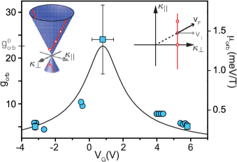
The orbital moment deduced from Fig. 14 corresponds by Eq. (13) to nm. This is surprisingly large for the chemical-vapor-deposited nanotube used in the experiment, for which nm is expected. Other experiments have measured a range of values for ; while some have obtained similarly large values Jarillo-Herrero et al. (2005a); Kuemmeth et al. (2008); Steele et al. (2013), other results are consistent with smaller-diameter nanotubes Minot et al. (2004); Makarovski et al. (2007); Churchill et al. (2009a). Although the discrepancy is not large, it is possible that expectations for either the nanotube diameter or the orbital need to be revised. Measurements on devices with independently measured diameters would allow the discrepancy to be explored.
III.6 Spin-orbit coupling
On first consideration, it might be expected that carbon, as the second lightest of all semiconductors, should have negligible spin-orbit coupling. Indeed, spin-orbit coupling is comparatively weak in free carbon ( splitting meV Kramida et al. (2013)), and almost completely suppressed near the Dirac points in flat graphene Min et al. (2006); Huertas-Hernando et al. (2006). However, it was realised by Ando (2000) that the suppression relies on the symmetry of graphene. In a nanotube, this symmetry is broken by curvature, leading to a coupling up to a few meV between the spin and orbital moment of electrons. This coupling, first detected by Kuemmeth et al. (2008), is the key to controlling spins in nanotubes electrically. This section explains in detail how it arises and how it is measured.
III.6.1 Origin of spin-orbit interaction in nanotubes
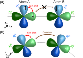
In atomic carbon, coupling between the total spin and orbital angular momentum adds a term to the Hamiltonian:
| (14) |
where is the atomic spin-orbit strength (From the atomic splitting quoted above, meV.) The effect of this coupling is to mix single-particle states with opposite spin from different orbitals, such as and . Whether this leads to spin-orbit coupling in the band structure depends on how it affects hybridization between orbitals in different atoms, which in turn depends on the crystal structure.
The contrasting situations in flat and curved graphene are illustrated in Fig. 15, which shows the atomic orbitals for two adjacent atoms and . Any effect on the band structure arises through the combination of intra-atomic spin-orbit coupling and inter-atomic hopping. In flat graphene (Fig. 15(a)), symmetry forbids direct hopping from a state on one atom to a state on another because and orbitals have opposite parity under inversion. Therefore atomic spin-orbit coupling between e.g. and states does not introduce any non-spin-conserving hybridization between and , and thus spin-orbit coupling in the band is second-order and in practice negligible.
This situation is changed in the presence of curvature, which breaks the inversion symmetry on which the above suppression relies (Fig. 15(b)). To understand this, it is convenient to work in the curved coordinate basis labelling radial, circumferential and axial directions, so that the band is composed predominantly of hybridised orbitals. Since the and orbitals are not orthogonal, hopping between them is allowed, leading to an indirect hybridization between and and consequently a spin-orbit coupling in the band.
As a result of this spin-orbit coupling, the effective hopping matrix element between and now contains both a direct and a spin-flip term. The interference between these terms causes a spin precession about the -axis, and a corresponding splitting of the two spin states within a given valley as though by a magnetic field directed along the nanotube. The spin-orbit splitting is defined as the Zeeman splitting due to this field, .
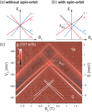
Figure 16(a-b) show the consequences of spin-orbit coupling for the band edges. Without spin-orbit coupling (Fig. 16(a)), the zero-field levels are four-fold degenerate, but are split in a magnetic field through a combination of Zeeman and orbital coupling. (This figure differs from Fig. 11(g) by the inclusion of Zeeman spin splitting.) Spin-orbit coupling splits each four-fold degenerate level at into a pair of two-fold degenerate levels (Fig. 16(b)); each element of the pair comprises a Kramers doublet, as required by time-reversal symmetry. The sign of determines whether parallel or antiparallel alignment of spin and valley magnetic moments is favoured. For , the magnetic moments of spin and valley of the lowest (highest) edge of the conduction (valence) band add, whereas they subtract for . (see Fig. 18 for examples.) For , as drawn here, spin-orbit coupling favours alignment of the spin and valley magnetic moments. The lower doublet therefore comprises the states for which both magnetic monts have the same sign, while the upper doublet comprises the states .
III.6.2 The discovery of nanotube spin-orbit coupling
Figure 16(c) shows excited-state spectroscopy of the first electron shell of an ultraclean nanotube as a function of magnetic field Kuemmeth et al. (2008). The positions in gate voltage of the first four conductance peaks provide a map of the lowest four energy levels, as explained in Appendix A.2 (which also explains how to convert from gate voltage (left axis) to energy (right axis)). The dependence of the energy levels on magnetic field arises from the combination of valley and spin magnetic moments in each level, as in Fig. 11(g), but taking account of the spin magnetic moment. From the line slopes, valley and spin quantum numbers can be assigned to each level (as in Fig. 16(a,b)).
The data are clearly consistent with Fig. 16(b) rather than Fig. 16(a). The key signature of spin-orbit coupling is the separation of the four spin-valley levels at zero field into two doublets. The magnitude of the splitting gives the spin-orbit coupling strength meV, corresponding to T. From the spin and valley assignments deduced from the line slopes, it is clear that in this case spin-orbit coupling favors states with parallel spin and valley magnetic moments.
III.6.3 Different types of nanotube spin-orbit coupling
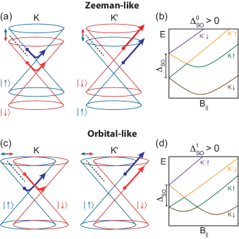
Detailed calculations of the spin-orbit coupling reveal that there are actually two terms in the spin-orbit Hamiltonian, corresponding to Zeeman-like and orbital-like coupling (Fig. 17). The Zeeman-like contribution, characterized by a parameter , can be visualized as a vertical shift of the Dirac cones that is opposite for the two spin directions (Fig. 17(a)). This is equivalent to an effective Zeeman shift of each spin state given by:
| (15) |
where and are defined at the end of Sec. III.5.1.
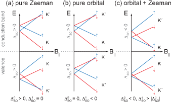
The orbital-like contribution to the Hamiltonian gives rise to a horizontal shift of the Dirac cones, similar to the curvature-induced shift discussed in Sec. III.3, but opposite for the two spin directions (Fig. 17(c)). This is equivalent to a spin-dependent magnetic flux coupling to the orbital moment. The horizontal shift of each cone is:
| (16) |
where parameterizes the strength of the coupling. In this case, the hole energy levels are no longer simply the negative of the electron energy levels at finite field, and the electron-hole symmetry is broken Kuemmeth et al. (2008).
Equations (15) and (16) can be combined with the graphene dispersion relation Eq. (1) and the magnetic field response Eq. (11) to give the Hamiltonian in terms of the spin and valley quantum numbers, including spin-orbit and magnetic coupling:
| (17) |
where is the spin operator (with eigenvalues ). Writing this Hamiltonian required the use of the Pauli operators , which act in a two-dimensional sublattice space describing the wave function amplitude on the two sublattices of Fig. 4. These are described in more detail in Appendix B. In Eq. 17, the horizontal and vertical shifts due to the two spin-orbit terms are evident.
The existence of two forms of spin-orbit coupling goes beyond the simple picture of Sec. III.6.1. The orbital-like contribution can be understood as a Rashba-type coupling, arising from the broken reflection symmetry about the graphene plane. A curvature-induced displacement of the orbitals gives rise to a radial electric field, which circulating electrons experience as a magnetic field proportional to the azimuthal component of their momentum. It is similar to the Rashba coupling predicted by Kane and Mele (2005) for graphene in an electric field, and is equivalent to a horizontal shift of the dispersion relation of the form in Eq. (16).
| Reference | ||||
| (theory) | (expt) | |||
| nm | eV | eV | eV | |
| Kuemmeth et al. (2008) | 5.0 | -120 | 120 | 370 (1e) |
| -240 | 0 | -210 (1h) | ||
| Churchill et al. (2009b) | 1.5 | -400 | 400 | 170 (1e) |
| Jhang et al. (2010) | 1.5555AFM measurement | -800 | 400 | 666Inferred from the magnetoresistance of an open CNT quantum wire. |
| Jespersen et al. (2011b) | 2.9777Derived from many-carrier regime but ignoring suppression of by confinement (Eq. (12)). These values of are therefore likely to be underestimates. | -210 | 210 | 150 (many e) |
| -410 | 0 | 75 (many h) | ||
| Lai et al. (2014) | -920 | 460 | ||
| (many e/h) | ||||
| Steele et al. (2013) | ||||
| Device 1 | 7.2 | -80 | 80 | 3400 (1e) |
| Device 2 | 6.8 | -90 | 90 | 1500 (1e) |
| Device 3 | 4.1 | -150 | 150 | -1700 (1e) |
| 3.7 | 0 | -320 | 1300 (1h) | |
| Cleuziou et al. (2013) | ||||
| Device 1 | -240 | |||
| (h, few shells) | ||||
| Device 2 | -340 (1e,3e) | |||
| Schmid et al. (2015) | -350 (17e) | |||
The Zeeman-like contribution also comes from a lack of reflection symmetry through the nanotube surface. In contrast to the orbital-like contribution, which is caused by the homogeneous part of the radial electric field, the Zeeman-like contribution comes from variation of the electric field within the graphene unit cell. In a tight-binding picture, this contribution can be thought of as curvature-induced spin-orbit scattering between next-nearest neighbours (e.g. from one site to another), whereas the orbital-like contribution comes from scattering between nearest neighbors (between an and a site). The perturbation theory leading to these separate effects is outlined in Appendix B.
The values of the coefficients and depend on the structure of the nanotube. The theoretical values are estimated as:
| (18) | |||||
| (19) |
These values are quite sensitive to the method of computation. The first calculations (Ando (2000), later refined by Yanik et al. (2004); Huertas-Hernando et al. (2006)) considered the modification of hopping amplitudes by atomic spin-orbit coupling which gives rise to the orbital-like contribution. Later work Izumida et al. (2009) calculated the spin-orbit correction in more detail using a non-orthogonal tight-binding calculation that incorporated the spin degree of freedom and used four orbital states per atom. This work was the first to predict the Zeeman-like contribution. The parameters and were estimated by Izumida et al. (2009) in two ways: by nearest-neighbour tight-binding using density-functional theory potentials, and by fitting to a full numerical model, from which (Eqs. 18-19) are taken. They have also been calculated by an extended tight-binding Slater-Koster method Chico et al. (2009) and using density functional theory combined with atomic spin-orbit coupling and tight binding Zhou et al. (2009). A similar calculation to Izumida et al. (2009) was performed by Jeong and Lee (2009), corroborating these results. The coefficients have also been estimated by Klinovaja et al. (2011a), who included the effects of external electric fields. These different methods differ quantitatively by a factor up to , but the dependence is dictated by symmetry.
Combining Eqs. (2,8,15,16) shows that both spin and valley are good quantum numbers in a magnetic field directed along the nanotube. The corresponding eigenenergies Jespersen et al. (2011b) are, again assuming a flat potential as in Eq. (12):
| (20) |
where is the bandgap at zero field without spin-orbit coupling and the upper (lower) sign refers to the conduction (valence) band. In the limit , this gives for the combined zero-field splitting:
| (21) |
The sign of can be deduced from the spectrum as follows (Fig. 18): If the two states converge with increasing field and eventually cross (as in Fig. 16), then ; if it is the states that cross, then Bulaev et al. (2008); Kuemmeth et al. (2008).
From Eqs. (18,19,21), four predictions can be derived:
-
1.
Spin-orbit coupling depends on chirality and diameter, hence different devices should display different coupling.
-
2.
The different terms lead to different behaviour when fields comparable to are applied (see Fig. 11). This can be seen by plotting the first four energy levels as a function of across the Dirac point. For orbital coupling (and assuming a residual bandgap remains), the lowest-energy level has a pair of minima (Fig. 17(d)), corresponding to the Dirac points crossing the quantization lines for spin up and spin down. For Zeeman-like coupling, the two minima occur in the first and second energy levels, as in (Fig. 17(b)).
-
3.
The orbital-like term contributes with opposite sign to for electrons and holes, thereby breaking electron-hole symmetry (because the hole energy levels are no longer a mirror image of the electron levels.) The Zeeman-like term by itself preserves electron-hole symmetry (Fig. 18(b)).
- 4.
Evidence for prediction (1) comes from measurements on several devices, presumably with a distribution of structures. The spin-orbit parameters are indeed found to take different values (Table 2), although it has not yet been possible to determine chiral indices in the same device for comparison. The spread of is in fact larger than expected from Eqs. (18-19), as discussed in Sec. III.8.
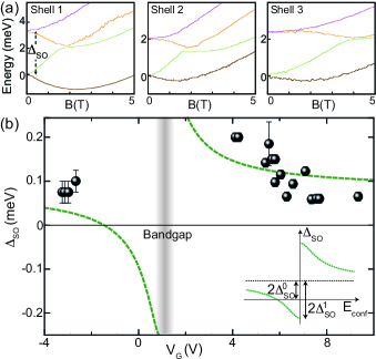
Testing prediction (2) experimentally requires a device where lies at an accessible field. Figure 19(a) shows ground-state spectroscopy of the first four Coulomb peaks in a device where this was achieved Steele et al. (2013). The pattern of energy levels clearly resembles Fig. 17(b) more than Fig. 17(d), suggesting that the coupling in this device is predominantly Zeeman-like.
Prediction (3) was confirmed in the first measurements by Kuemmeth et al. (2008), who found to be different in both magnitude and sign for the first electron and first hole. Further confirmation, and a test of prediction (4), was obtained in a different device where could be measured across several shells of electrons and holes Jespersen et al. (2011b). As seen in Fig. 19(b), decreases with higher , qualitatively consistent with Eq. (21) assuming an orbital contribution. For the shells measured in this device, did not change sign between electron and holes, providing further evidence of a Zeeman-type contribution.
III.6.4 Uniform electric fields
As well as intrinsic spin-orbit coupling from the nanotube structure, there is also predicted to be an extrinsic coupling due to electric fields Klinovaja et al. (2011a). This is a form of Rashba effect, and leads to a shift of the Dirac cones in by an amount
| (22) |
where is the electric field (perpendicular to the nanotube) and is the spin component perpendicular both to the nanotube and to . The parameter , which governs the strength of this effect, is uncertain because it depends on several numerically calculated band structure parameters, but is estimated as nm Klinovaja et al. (2011a). This Rashba-like coupling has not yet been observed, but in principle allows for all-electrical spin manipulation Bulaev et al. (2008); Klinovaja et al. (2011b).

III.7 Intervalley scattering
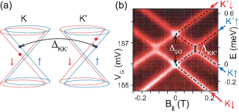
In quantum dots (i.e. confined states), magnetospectroscopy as in Fig. 16 allows measurement of a phenomenological parameter that governs the strength of avoided level crossings between opposite valley states. This was observed by Kuemmeth et al. (2008) in a suspended one-electron quantum dot for which was found (Fig. 20(b)). Although this splitting indicates scattering between states in different valleys with the same spin, it does not reveal a specific mechanism. Experiments performed on top-contacted nanotubes showed as small as Churchill et al. (2009b), and Jespersen et al., 2011b reported significant fluctuations within a device with no obvious correlation to gate voltage or occupation number. Grove-Rasmussen et al., 2012 investigated the suppression of mixing by application of a parallel magnetic field. Although has been used in other works as a empirical fitting parameter Pei et al. (2012); Lai et al. (2014), the microscopic origin has not been investigated. In particular, all experiments involved finite tunneling to the source or drain electrode, and hence the intrinsic valley coupling in closed quantum dots has yet to be measured.
Historically, we suspect that electrical disorder on the scale of the interatomic spacing, leading to comparatively large , was the main reason for the decade-long delay between the first nanotube quantum dots and the discovery of spin-orbit coupling. As evident below, values larger than obscure the signatures of spin-orbit coupling. It was only the development of low-disorder fabrication techniques that allowed such a delicate effect to be identified.
III.7.1 Putting it all together
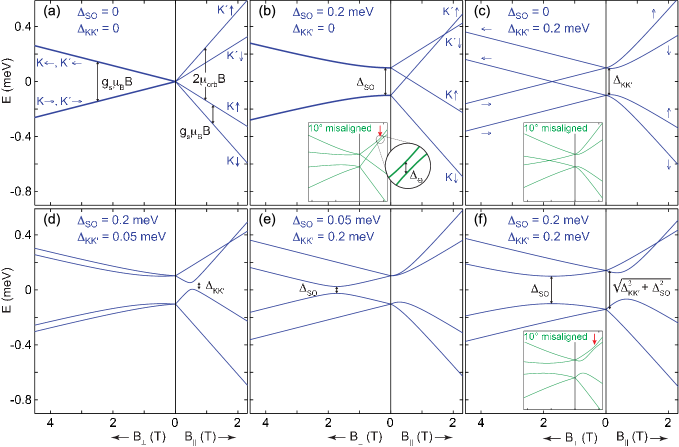
Figure 21 shows calculated spectra in a single electron shell as a function of magnetic field in both perpendicular and parallel directions for a range of values of and . This calculation proceeds by first working out the eigenenergies for a magnetic field directed along the nanotube and in the absence of disorder. Under the assumption that there is no mixing of electron and hole shells, i.e. in the limit
| (23) |
Eq. (20) reduces to:
| (24) |
where is the energy without magnetic field or spin-orbit coupling.
Introducing disorder or tilting the field relative to the nanotube axis by angle (so that ) mixes the eigenstates. In the basis , the Hamiltonian is:
| (25) |
Figure 21 shows the numerically calculated eigenstates of this Hamiltonian. With no spin-orbit or disorder (Fig. 21(a)), the four states are degenerate at zero field, being split through a combination of orbital and Zeeman coupling. Pure spin-orbit coupling (Fig. 21(b)) splits the zero-field quadruplet into two doublets; note that in small perpendicular field, Zeeman coupling is ineffective, because the spin states are locked to the valley, and valleys are not coupled. Pure disorder (Fig. 21(c)) suppresses orbital coupling at low field, but preserves the Zeeman splitting in both field directions.
| Quantity | Expression | Value | Reference |
|---|---|---|---|
| Confinement bandgap | 0.70 eV/ [nm] | Charlier et al. (2007) | |
| Curvature bandgap | Izumida et al. (2009) | ||
| Strain bandgap | Huang et al. (2008) | ||
| Torsion bandgap | Yang and Han (2000) | ||
| Effective mass | |||
| Orbital magnetic moment | 0.20 meV/T [nm] | Ajiki and Ando (1993) | |
| [nm] | |||
| Zeeman magnetic moment | 58 eV/T | ||
| Spin-orbit coupling | Izumida et al. (2009) | ||
| (see Appendix B) | Izumida et al. (2009) | ||
| Electric field spin splitting | Klinovaja et al. (2011a) | ||
| Intervalley scattering | eV (typical) | Kuemmeth et al. (2008) | |
| Longitudinal mode spacing | Tans et al. (1997) | ||
| (high-energy limit) |
In cases where both terms are finite but one dominates, the smaller parameter leads to anticrossings (Fig. 21(d-e)). Finally, if the two terms are of comparable finite magnitude, a complex spectrum emerges showing a mixture of effects (Fig. 21(f)). A small misalignment of the nanotube relative to the field axes, illustrated in the insets, introduces an anticrossing between the upper two levels. The magnitude of the anticrossing is .
This picture is confirmed in Fig. 22 for a device with comparable and . The energy levels were measured by cotunneling spectroscopy, which maps out energy differences between ground and excited states (see Jespersen et al., 2011b for discussion of this experimental technique). The resonant transitions appear as peaks or dips in whenever is equal to the difference of energy levels. The measured transitions (Fig. 22(a)) as a function of perpendicular and parallel field agree well with the predicted level differences (Fig. 22(b)) from the spectrum (Fig. 22(c)), calculated in the same way as in Fig. 21 assuming . In particular, the curvature of energy levels in parallel field due to mixing and the anticrossing in perpendicular field due to are seen. From similar data the parameters and can be measured precisely over a wide range of electron and hole occupation Jespersen et al. (2011b).
We conclude this section by summarizing, with best numerical estimates, the various nanotube band structure parameters discussed in the text (Table 3). Experimentally, one set of parameters usually suffices to characterize an entire shell, implying that these parameters are not strongly affected by addition of a few extra electrons. This is as expected from the constant-interaction model, which assumes all interactions can be parameterized by a single constant capacitance (Appendix A).
III.8 Open questions
Comparison of theoretical and experimental spin-orbit coefficients shows serious discrepancies. As shown in Table 2 different devices give unexpectedly large variation. With the diameters inferred from , Eqs. (18-19) predict that should range up to eV. Instead, values as large as meV have been reported, with several devices yielding results up to sixteen times larger than expected Jhang et al. (2010); Steele et al. (2013). Other experiments have found within the expected range Churchill et al. (2009b); Lai et al. (2014); Cleuziou et al. (2013). Furthermore, in some cases the calculations even predict the wrong sign for both couplings and Kuemmeth et al. (2008); Jespersen et al. (2011b).
This is clearly an open question for both theory and experiment. One explanation might be uncertainty in the tight-binding overlap integrals, which enter Eqs. (18-19) as empirical input parameters. Alternatively, electron interactions (Sec. VII.2.2) may play a role Rontani (2014). Another possibility is that some other symmetry-breaking between inside and outside the nanotube is responsible for the observed couplings, such as gate dielectric or adsorbates. For example, hydrogen adsorbed onto graphene is known to enhance the spin-orbit coupling Balakrishnan et al. (2013). In nanotube devices, adsorbed water affects the current-voltage characteristics Kim et al. (2003), although it is uncertain whether this is directly by modifying the band structure Na et al. (2005) or through another mechanism such as gathering ions from the environment Sung et al. (2006).
A possibly related effect is that diameters inferred from measured are sometimes unexpectedly large. Whereas chemical-vapor deposited nanotubes are expected to have nm, values of corresponding to nm have been measured Minot et al. (2004); Kuemmeth et al. (2008); Jarillo-Herrero et al. (2004, 2005a). However, other devices yield values in the expected range Minot et al. (2004); Makarovski et al. (2007); Churchill et al. (2009b); Deshpande and Bockrath (2008). Measurements on nanotubes with known chirality should help clarify these discrepancies. Interestingly, the prediction of complete band closing at (Fig. 11) is not borne out by experiments, which typically find minimal bandgaps meV. This hints at physics beyond the single-particle picture discussed here, such as formation of a Mott gap Deshpande et al. (2009) or an excitonic insulator Rontani (2014).
A separate set of questions addresses how to take advantage of the spin-orbit interaction. Ideas in this direction such as spin filtering and detection Mazza et al. (2013); Braunecker et al. (2013), generation of helical states Klinovaja et al. (2011b) and spin-orbit mediated spin control Flensberg and Marcus (2010); Bulaev et al. (2008) have already emerged (the latter is the topic of Sec. V.3.3).

IV Double quantum dots and Pauli blockade
Transport through a single quantum dot involves an electron from the Fermi sea in one lead that tunnels via a discrete quantum state to an empty state in the other lead. For two dots in series an additional tunneling event occurs which involves a transition from one particular initial quantum state to a particular final state. This dot-to-dot transition is sensitive to selection rules, which determine the transition probability. The selection rules for nanotubes are based on the spin and valley quantum numbers. Whether they are obeyed in an experiment depends on to what extent spin and valley are good quantum numbers and how this is affected by spin-orbit coupling, hyperfine interaction or disorder. This sensitivity makes double quantum dots a versatile platform for studying quantum states and relaxation processes in nanotubes (Fig. 23).
IV.1 Role of bandgap and electron-hole symmetry in charge stability diagrams
IV.1.1 Theory
A double quantum dot formed by two dots in series defined within the same nanotube has similarities and differences to double dots defined in conventional semiconductors reviewed by Wiel et al., 2002; Ihn, 2010. Analogous to Fig. 53, the device can be modelled by an electric circuit (Fig. 24(a)). If each of the tunnel barriers is sufficiently opaque, , then the charge within each dot is quantized and the number of electrons can only change at specific gate voltages. A graph of the equilibrium charge configuration as a function of gate voltages is called a stability diagram (Fig. 24(b)). The size of each region is a measure of the addition energy (Eq. (42)), horizontally for adding an electron in the right dot and vertically for an addition to the left dot. In most semiconductor dots either the electron or hole region is accessible. In narrow-gap nanotubes the gate coupling can be sufficient to cross the bandgap, evident as larger honeycombs, and enter both regions. Because of the approximate electron-hole symmetry, a similar honeycomb pattern is expected in all regions of the stability diagram. Interestingly, the inter-dot tunnel barrier in the () and () regions is formed by a junction.
IV.1.2 Experiment
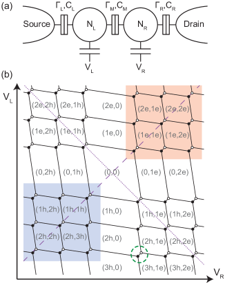
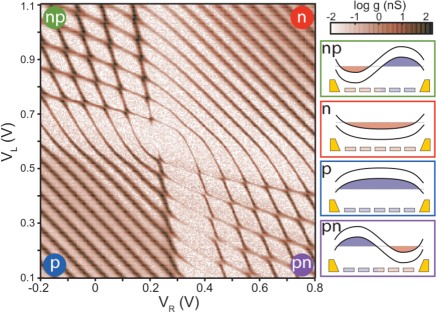
The electron-hole stability diagram expected from Fig. 24 is most easily observed in narrow-gap nanotubes. Full control over the basic parameters of a double quantum dot, namely charge occupation (, ) and tunnel couplings (, , ), requires at least five gate electrodes, and so the full charge stability diagram is at least five-dimensional. A two-dimensional cut is shown in Fig. 25. Here the conductance through the device is plotted as a function of control parameters and . Figure 25 demonstrates that an actual device can show a stability diagram that is strikingly different from the diagram of Fig. 24, characteristic of the weak-coupling regime. In Fig. 25, the middle gate voltage was intentionally chosen such that electron-hole double dots and single dots with electron or hole filling were demonstrated within the same device. In this regime, cotunneling processes give a significant contribution to transport, and hence boundaries between Coulomb valleys as well as triple points show up as conductance features. Note both the spatial and electron-hole symmetry displayed by the data (mirror symmetry about the and diagonal respectively), attesting the cleanliness and tunability of suspended devices as in Fig. 3(f).
If the tunnel rates are too small to measure conductance, the charge stability diagram can be studied by charge sensing. Such capacitive sensing techniques are useful for the readout of pulsed-gate experiments on closed double dots and qubits Churchill et al. (2009b), as well as for investigating the quantum capacitance associated with electron interactions and correlations Ilani et al. (2006).
Many other regimes are possible in double quantum dots. For example, a sizable longitudinal level spacing in each dot can result in an overall eight-electron shell structure Jørgensen et al. (2008), whereas strong interdot tunneling lifts charge quantization within each dot, which can be interpreted as the formation of delocalized molecular states Gräber et al. (2006). Devices with ambipolar charge stability and a high degree of tunability have been used to study many phenomenona, including Wigner crystallization Pecker et al. (2013), Klein tunneling Steele et al. (2009b), and tunable electron-phonon coupling Benyamini et al. (2014)
IV.2 Spectroscopy of energy levels in bias triangles
Increasing the source-drain bias across a double dot allows non-linear conductance to be probed, providing spectroscopic information on the energy levels. Applying a bias large enough to overcome Coulomb blockade expands the triple points to finite-bias triangles. These triangles serve as a powerful experimental tool to reveal a variety of quantum effects in nanotubes. Figure 26(a-c) shows their evolution with increasing . Pairs of bias triangles start to overlap once becomes larger than the mutual charging energy of the double dot888Details can be found in Wiel et al. (2002) or Ihn (2010).. The finite bias breaks the left-right symmetry of a nominally symmetric device, yielding triangles pointing along the diagonal with a direction depending on the sign of . In panels (a-c) the sign of has been chosen so that electrons flow from the left contact (source) to the right contact (drain).
Under appropriate conditions, excited states (in either dot) are evident as discrete lines within a bias triangle. If interdot tunneling is the rate-limiting process, these lines appear parallel to the base of the triangles, but only if both tunnel rates to the leads remain at the same time smaller than level spacing and bias (). From the line separation, measured from the base of the triangles, the corresponding excitation energies can be deduced. Examples from three different devices (Fig. 26(d-f)) show the expansion of the bias triangles with and the appearance of excited-state lines999Figure 26 uses instead of for data with a different source-drain or left-right convention from Fig. 24a..
IV.3 Pauli blockade involving spin and valley
IV.3.1 Motivation
The dot-to-dot transitions in conventional double dots are strongly regulated by selection rules. These selection rules arise from the Pauli exclusion principle, and can provide insight into the robustness of quantum numbers in the two dots and during interdot tunneling. Since in nanotubes both spin and valley can form approximate good quantum numbers even in the presence of spin-orbit coupling, the manifestations of Pauli blockade and Pauli rectification are more complex than in conventional semiconductors. In this section, we briefly review Pauli blockade in conventional semiconductors with only twofold spin degeneracy to establish useful terminology. Next, we extend the model by adding twofold valley degeneracy to illustrate the persistence of Pauli blockade beyond spin blockade. In order to make connection to actual nanotube experiments, we then discuss the main effects of spin-orbit coupling and electron-electron interactions on two-electron states within a quantum dot. Finally, we present experimental evidence for Pauli blockade in nanotubes, and discuss the roles of spin, valley, and hyperfine coupling.
IV.3.2 State counting and Pauli blockade
Pauli blockade is well established in conventional quantum dots containing a total of two electrons Ono et al. (2002); Hanson et al. (2007). It relies on the fact that the (0,2) ground state is non-degenerate (it is a spin singlet) and is well separated in energy from the lowest spin triplet states, as illustrated in Fig. 27(a). The spin triplet states are antisymmetric in their orbital degree of freedom with respect to electron transposition, and hence necessarily involve an excited single-particle state. Therefore, the energy cost to form the Triplet101010We capitalize Triplet and Singlet whenever we refer to specific spin-singlet and spin-triplet states indicated in Fig. 27. (0,2) states, is approximately the single-particle level spacing in the right dot modified by electron interactions (cf. discussion of in Fig. 28(a)). This is in contrast to the Triplet (1,1) states, which for small interdot tunneling are nearly degenerate with the Singlet (1,1). If the (0,2) splitting is larger than temperature, then a Triplet (1,1) state cannot easily transition into the (0,2) state. If the applied source-drain bias is also larger than temperature, then the Triplet (1,1) is long-lived, and its occupation suppresses current flow due to Coulomb blockade. This effect is known as spin blockade, and manifests itself in current rectification (Pauli rectification).
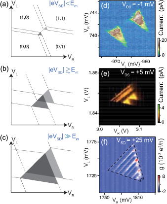
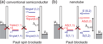
In nanotubes, the two-electron spectrum is richer due to the two valleys. Ignoring spin-orbit coupling for clarity, it is schematically shown in Fig. 27(b). Anticipating the breakdown of spin-singlet and spin-triplet terminology due to spin-orbit coupling, we have labeled the states according to the symmetry of the longitudinal quantum numbers under electron exchange ( or as defined below). As we will see, Pauli blockade is nevertheless possible in nanotubes. Even in the presence of spin-orbit coupling and small valley scattering, the projections of spin and valley in Eq. (25) can remain (approximate) good quantum numbers, for example in the presence of a parallel magnetic field111111Even in the absence of good quantum numbers Pauli rectification behavior can still occur, due to Kramers degeneracy. This was theoretically exemplified for double dots with strong spin-orbit coupling by Danon and Nazarov, 2009.. As in panel (a), interactions alter the spectrum, and the splitting between the symmetric ground states and antisymmetric excited states is given by the level spacing modified by an interaction energy.
Figure 28 shows a simple state-counting argument leading to the degeneracies indicated in Fig. 27(a-b) for the (0,2) states. For conventional semiconductors we consider two spin-degenerate levels separated by a level spacing . The non-degenerate ground state, Singlet (0,2), is formed by two electrons occupying the lower level (lower panel). If each level is occupied by only one electron, then four degenerate states are possible (upper panel). Exchange interactions (INT) result in an energy splitting between the Singlet′ (0,2) and Triplet (0,2) states, thereby reducing slightly Kouwenhoven et al. (2001).
The case of two fourfold degenerate nanotube shells is shown in Fig. 28(b). The lower shell can be occupied by two electrons in six ways, while 16 different states are possible with one electron in each shell121212The multiplet representing two electrons in the upper shell is not shown in Fig. 28(b).. Analogous to conventional semiconductor quantum dots and to lowest order, electron interactions (INT) split the 16 states into 10 longitudinal antisymmetric (lower energy) and 6 longitudinal symmetric states (higher energy). In the framework of first-order perturbation theory, this can be understood by calculating the (long-range) exchange integral associated with each two-electron basis state, and noticing that it differs between states and states (Appendix B.8). The complexity of the nanotube energy spectrum compared to conventional semiconductors is further revealed by turning on spin-orbit coupling within each multiplet (SO), as shown by the rightmost panel of Fig. 28(b) and discussed further below.
State-counting arguments similar to those presented for (0,2) lead to symmetric and antisymmetric states in the (1,1) configuration. Formally, this is accomplished by redefining the excited shell of the right dot as the lowest shell in the left dot: , . In the limit of vanishing interdot tunneling, interactions in the (1,1) regime can be neglected ().
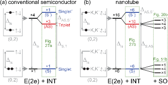
IV.3.3 Symmetric and antisymmetric multiplets in nanotubes - theory
| Longitudinally symmetric states | |
|---|---|
| Designation | Energy |
| Longitudinally antisymmetric states | |
| Designation | Energy |
| Longitudinally symmetric states | |
| Designation | Energy |
To gain more insight into the two-electron states in the presence of spin-orbit interaction131313Related theoretical treatments are found in Reynoso and Flensberg (2011, 2012); von Stecher et al. (2010); Weiss et al. (2010)., we first consider the quantum numbers relevant for the lowest longitudinal symmetric multiplet , i.e. two electrons occupying the lowest shell in the right quantum dot. The valley, spin (and longitudinal) quantum numbers are listed in Table 4, with the states organized according to their energies. The two-electron energy within the constant interaction model is found by adding the single-particle energies and a charging energy :
| (26) |
where specifies the lowest shell in the right dot and and are the valley and spin quantum numbers of the two electrons. The states are calculated by the method of Slater determinants, but taking account of the fact that , , and are coupled.
Our conventions for labeling two-electron quantum states are stated below the three bold table headers. For example, consider the state denoted , which is spin- and valley-unpolarized. Written out explicitly, the energy and the state are141414See Appendix B for a more thorough derivation of the basis used.:
| (27) | |||||
where the subscripts on the right of Eq. (LABEL:S(0,2)state) refer to electron 1 or 2, and the three labels in a single-particle state are the longitudinal shell, valley and spin quantum numbers associated with that electron. The states in Table 4 are classified as longitudinally symmetric or antisymmetric according to whether the wave function remains the same or changes sign under the interchange . Thus the example in Eq. (LABEL:S(0,2)state) is symmetric (). We do not decompose further into a product of longitudinal, valley, and spin wave functions, as this is strictly correct only at and in the absence of spin-orbit coupling151515This decomposition can be illustrative (e.g. in Pecker et al., 2013; Pei et al., 2012), but is unsuitable for accurate calculations.. In general, the longitudinal wave function depends on both and Weiss et al. (2010).
Next we consider two-electron states with one electron in the lowest shell () and one electron in the first excited shell (). By a similar procedure, sixteen distinct Slater determinants can be written. However, some of them are coupled by electron interactions (“INT” in Fig. 28(b)), resulting in the splitting and modifying (see VII.2). The eigenstates of the electron interactions are the ten antisymmetric states () and six symmetric states () formed by linear combination of the Slater determinants. These eigenstates are listed with their energies in Table 4.
As for , the energies at are found by adding the single-particle energies, charging energy, and interaction energy. However, the expressions for the explicit states now contain four terms. For the spin and valley polarized states (), these four terms reduce to a simple two-term Slater determinant, but for the remaining six and six states this is not the case due to the interactions . This tells us that in general Eq. (26) is too simple to predict the spectrum accurately. In particular, it does not take magnetic fields into account, nor differences in spin-orbit coupling and valley scattering between different shells, not to mention short or long range interactions discussed in Sec. VII. As an example, the energy and quantum state of the spin-valley unpolarized state denoted by are:
| (29) | |||||
The longitudinal antisymmetry of this state is easily seen by comparing terms in the same row of Eq. (LABEL:ASstate), while comparing between rows shows the symmetry of the spin-valley part. The spin-valley unpolarized state (also denoted ) involves the same single-particle states, but is obtained by changing the longitudinal symmetry, i.e. by changing the sign on the second and third terms in Eq. (LABEL:ASstate).
All relevant two-electron states in (1,1) can also be constructed from Table 4, simply by identifying with , and with . This works by assigning to the lowest shell in the right (left) dot, and setting level spacing and interactions to zero. We call antisymmetric states “blocked” states, because they vanish formally when setting . Physically, this means that these states cannot be converted into charge states without involving a higher orbital in the right dot or changing their spin or valley configuration. The states generated in this fashion (along with the states) from Table 4 are useful basis states for a tunnel-coupled double dot at , assuming that the spin-orbit coupling in the two dots is identical 161616In , the splitting between symmetric states and antisymmetric states vanishes for small interdot tunneling, , and hence a different basis would be used, appropriate for the regime . Similarly, different orbital moments in left and right dot would require a different basis at sufficiently large magnetic field. .
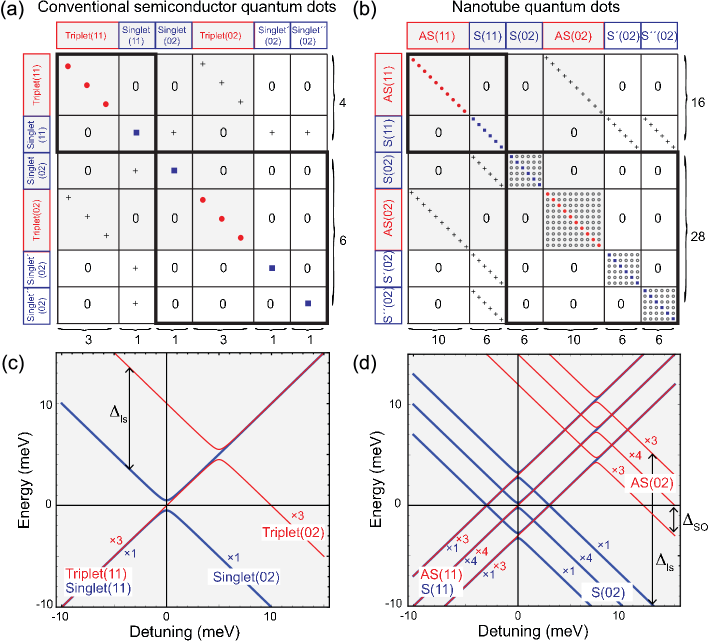
Having introduced all relevant (1,1) and (0,2) multiplets, a useful overview of the states and their mutual coupling is obtained by setting out the Hamiltonian in matrix form. Figure 29 shows schematic matrices for (a) a conventional semiconductor double dot in the spin-singlet/spin-triplet basis, and (b) a nanotube double quantum dot in the basis of the longitudinal symmetric/antisymmetric multiplets. These matrices can be divided into submatrices coupling manifolds of particular symmetry. In conventional semiconductors all submatrices are diagonal even when interactions are included. Tunnel coupling between states of the same singlet/triplet character is reflected (+ symbols) in the submatrices between (1,1) and (0,2) states. In nanotubes, the overall structure is similar, but the number of states in each multiplet is increased and the diagonal elements now include spin-orbit coupling. Again, states with identical symmetry are coupled by diagonal tunnel matrices, and weak interactions (denoted above) appear as diagonal elements that shift the energies of multiplets with respect to each other. However, off-diagonal elements are allowed in the (0,2) multiplets ( symbols), although arguments can be made that these are small (Appendix B). Interactions within the multiplet (not included in Table 4) appear as diagonal and off-diagonal matrix elements, and are further discussed in Sec. VII.
Plots of energy versus detuning for the low-energy states (Singlet, Triplet and ) are shown in Fig. 29(c-d) neglecting interactions (). The more complex spectrum for the nanotube is clearly revealed. Valley mixing (assumed zero in this figure) would lead to additional avoided crossings (off-diagonal elements in the matrix) between states with different valley quantum numbers. The non-avoided crossings between the and states signify long-lived (1,1) states that give rise to Pauli blockade.
Tunneling from a blocked state to a state requires a change of the longitudinal symmetry. For some states this may simply involve dephasing between the left and right single-particle states. For other states it also necessitates a change in quantum numbers of at least one electron. In particular, we distinguish lifting of Pauli blockade by:
-
•
Dephasing only
-
•
Valley flips
-
•
Spin flips
-
•
Spin and valley flips
Inspection of all ten states reveals that a single flip in one of the dots can result in an unblocked double dot configuration. For some states it involves a spin flip, for others a valley flip (see examples in B.10). However, these single flip processes do not conserve energy because of spin-orbit coupling, and therefore cannot lift the blockade. Therefore, simultaneous spin-and-valley flips can become the rate-limiting process (“spin-valley blockade”).
To investigate which type of blockade is observed in experiments, careful identification of the involved states and quantum numbers is required. This is best facilitated by application of a magnetic field. In Fig. 30(a), the energies of the two lowest single-particle shells are plotted against parallel magnetic field. The two-electron magnetic moments are obtained by summing the one-electron magnetic moments (Fig. 30(b)). As an example, the filled circles in Fig. 30(a) indicate the two single-particle energies summed to give the energy of the state as in Fig. 30(b). Similarly, the empty circles indicate the two-single-particle energies combining to give the state denoted . The field dependence of the remaining states is found in a similar fashion. The states can be divided into pairs of valley-polarized, spin-polarized and spin-valley unpolarized states. Although all degeneracies of the two multiplets are lifted at finite field, and spin and valley quantum numbers can in principle be assigned based on the observed magnetic moment171717This requires that interactions have lifted the degeneracy with the multiplet not included in Fig. 30(b)., the spectroscopic intensity associated with each state can be very different, depending how exactly the spectrum is measured. The solid lines in Fig. 30(b) indicate the available two-electron states within the and multiplets, given that one electron occupies the state. These two-electron states are relevant when measuring the addition spectrum given that the first electron is in its finite-field ground state .
IV.3.4 Symmetric and antisymmetric multiplets in nanotubes - experiment
The two-electron spectrum can be measured by high-bias spectroscopy near the (0,1)-(0,2) transition. Assuming that the device starts in the (0,1) ground state (), then exactly three states of the symmetric two-electron multiplet can be reached and four states of the antisymmetric multiplet (Fig. 30(a)). All other two-electron states would require a higher-order process, in which the incoming electron also promotes the resident electron to change its spin or valley quantum numbers. The expected addition spectrum is shown in Fig. 31(b), and the corresponding data in Fig. 31(c). Although the qualitative agreement is quite good, the data shows a surprisingly small multiplet splitting meV, significantly less than the measured single-particle level spacing of 7.8 meV. This is due to strong electron-electron correlations (Sec. VII), that differ drastically from the weak exchange interactions typical in GaAs dots. This is of practical importance because a small splitting makes it difficult to observe Pauli blockade in nanotubes.
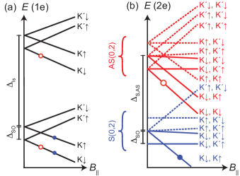
IV.3.5 Pauli blockade in nanotubes - experiment
Generally, interdot transitions that are forbidden by spin or valley selection rules are of particular interest, because measurements of leakage current or double-dot charge state then illuminate spin dynamics and spin-valley relaxation processes. We return to this topic in Sec. V. Although aspects of Pauli blockade in nanotubes have been observed by multiple groups, this phenomenon is experimentally less generic than in GaAs. A detailed understanding of the data is complicated by the large number of states involved (see Fig. 29), and often a lack of knowledge of critical device parameters such as differences in intervalley scattering or spin-orbit coupling between left and right dots, and the strength of electron-electron correlations. All these were neglected in Fig. 29.
Even the simplest manifestation of Pauli blockade, namely Pauli rectification in a DC transport experiment, can be obscured by other effects such as strong electron-electron correlations. In Fig. 27 we outlined the double dot energy levels for the transition and noted the importance of sufficiently large . In the () and () regimes, is limited by the level spacing from the longitudinal quantization , and likely significantly reduced by correlation effects . In order to keep as large as possible, the bandgap of the nanotube can be used as an effective large “level spacing”, making the observation of Pauli blockade more robust against interaction effects. The transition between and (dashed circle in Fig. 24(b)), is one example where the level spacing is enhanced by the band structure gap, .
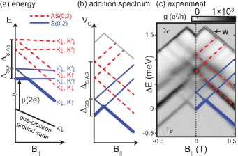
As shown in Fig. 32, rectification behavior for such a transition is observed for detunings as high as the applied bias voltage ( mV). This is larger than the spin-orbit splitting and estimated level spacing in this device Pei et al. (2012). This observation of strong current suppression up to high bias can be linked to the advantageous use of the band gap (see Fig. 33(a)).
In the blocked bias triangle of Fig. 32(b), a small increase of leakage current is observed at a detuning of approximately meV. This can be interpreted as a weak lifting of Pauli blockade, but a quantitative understanding of this leakage current, and identification of the corresponding relaxation rates, has not been reached. We speculate that it is necessary to include interaction effects beyond the constant interaction model to explain such features.
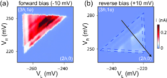
IV.3.6 Spin-valley blockade
Information about the role of spin and valley quantum numbers in the Pauli rectification of Fig. 32 can be obtained by applying a parallel magnetic field. If this induces an energy-level splitting larger than the interdot tunnel coupling or the intervalley scattering, we expect orbital and Zeeman couplings to restore valley and spin quantum numbers within the two-electron states. In turn we can associate these with the quantum numbers of single-particle levels.

In Fig. 33(c), the leakage current is measured as a function of detuning (defined in Fig. 32(b)) and . The base of the bias triangle (detuning ) corresponds to the ground state-to-ground state transition between and . Energy conservation imposes spin and valley selection rules for this transition, and therefore the leakage current provides information about the relaxation of these selection rules.
Figure 33(a) shows the assignment of single-particle quantum numbers to the highest (lowest) longitudinal shell in the valence (conduction) band of the left (right) quantum dot. These quantum numbers were inferred from the magnetic field dependence of the stability diagram181818To avoid confusion, we show quantum numbers of electronic states, even for the valence band. Other publications may consider the absence of a electron in the valence band as a hole, due to conservation of angular momentum. Quantum numbers in Pei et al. (2012); Steele et al. (2013) are not consistent with our identification.. Based on the single-particle picture, the ground state of is expected to make a transition from to as a function of parallel magnetic field191919Table 4 should not be used to generate these states, because conduction band and valence band differ in their assignment of and (Fig. 18).. This implies that at low field the ground state-to-ground state transition requires a spin flip of the right electron, whereas at higher magnetic field it requires a spin flip and a valley flip (compare the two arrows in Fig. 33(b)). Therefore, if valley is a good quantum number and conserved during interdot tunneling, then one expects the ground state leakage current at high field to be smaller than at low field. Indeed, this is seen in panel (c) by comparing conductance features marked with line 1 and line 2. We mention that the ground state is not a blocked state in the sense of Sec. IV.3.3: We can write it as a Slater determinant of one electron in the left () orbital and one electron in the right () orbital, , which does not vanish under the substitution (i.e. ). We therefore expect that relaxation to the charge state is allowed without involvement of higher orbitals or change of spin or valley configuration. The absence of this charge relaxation (line 3 in panel (c)) is not understood.
In summary, this data suggests that both spin and valley can contribute to Pauli blockade, but a quantitative understanding of the leakage current and relaxation rates has not been reached. We speculate that several mechanisms contribute, such as disorder, hyperfine coupling, spin-phonon coupling, or bend and spin-orbit mediated relaxation.
IV.4 Lifting of Pauli blockade by hyperfine coupling
In this section we investigate double dots where Pauli blockade is partially lifted due to hyperfine interaction between the electron spin and the 13C nuclear spins.
IV.4.1 Theory
Hyperfine interaction with disordered nuclear spins, such as 13C isotopes, couples different spin states by flip-flop processes and, in addition, different valley states, because of the atomically sharp length scale. It is therefore expected that hyperfine coupling generically lifts Pauli blockade and results in spin relaxation and spin dephasing processes. This mechanism of spin relaxation was considered by Semenov et al. (2007), whose numerical estimates predicted a spin relaxation time s. Relevant for quantum dot experiments in nanotubes, Yazyev, 2008; Fischer et al., 2009 inspected the role of dipolar and Fermi contact interaction in -hybridized nanostructures, resulting in an interesting interplay between isotropic and anisotropic hyperfine interactions.
In the tight-binding picture of Pályi and Burkard (2009), the hyperfine interaction with 13C is modeled by a matrix element that arises on the site of each nuclear spin (Fig. 34). Because it acts locally at each atomic lattice site that contains a 13C, hyperfine interaction couples not only to the electron spin, but also mixes the valley index (cf. discussion of valley scattering in Fig. 6). The strengths of the valley-conserving and valley-mixing parts of the effective hyperfine coupling were estimated to have the same order of magnitude. Pauli blockade, even in its strongest form protected by spin and valley (Sec. IV.3.6), can therefore be lifted by the presence of 13C atoms. Pályi and Burkard, 2009 considered the situation where valley scattering is dominated by hyperfine coupling. Ignoring spin-orbit coupling, they showed that the leakage current in the Pauli blockade regime of a double quantum dot is only strongly suppressed if both valley and spin splittings are larger than the hyperfine coupling.

The other limit, where valley scattering is dominated by disorder-induced valley scattering, was considered subsequenctly Pályi and Burkard (2010). Ignoring hyperfine coupling, but assuming strong SOI (larger than the splittings due to disorder and interdot tunneling), it was predicted that the current in the Pauli blockade regime can show a dip at low fields. Although similar to experimental data discussed in Fig. 35d, the amplitude of the predicted dip is orders of magnitude smaller than observed. In the theory, the low-field dip occurs because a difference in the valley coupling splittings diminishes the matrix element for tunneling, while at high fields the valley mixing is suppressed.
IV.4.2 Experiment
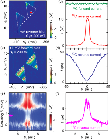
Figure 35 shows electron transport through weakly tunnel-coupled, Pauli blocked double dots. Panels (a-b) show the asymmetry in forward and reverse bias for a nanotube enriched with 13C, similar to the Pauli blocked 12C device discussed in Fig. 32. Figure 35(c) compares the magnetic field dependence of the reverse-bias leakage current near the base of the triangle with the forward current in the same tuning. Whereas the forward current is independent of applied magnetic field (indicating that the rate-limiting tunnel barrier, , is independent of magnetic field), the reverse leakage current is strongly suppressed only above a characteristic magnetic field scale, mT (Fig. 35(c)).
Churchill et al., 2009a attributed the current peak at to spin relaxation via electron-nuclear flip-flops, similar to the situation in GaAs double dots and InAs nanowires Koppens et al. (2005); Nadj-Perge et al. (2010b). Because of the mismatch of electron and nuclear magnetic moments, these energy-conserving flip-flop processes are expected to be strongly suppressed once the difference in Zeeman splitting exceeds the strength of the hyperfine coupling . Estimating the number of nuclei, , electron g-factor , and assuming uniform coupling to a Gaussian-distributed Overhauser field, , an effective hyperfine coupling constant – eV can be estimated. This is two orders of magnitude larger than predicted for nanotubes Yazyev (2008); Fischer et al. (2009) or measured in fullerenes Pennington and Stenger (1996).
This puzzling result stimulated theoretical work by Coish and Qassemi, 2011, who examined the role of thermally activated spin-flip cotunneling in lifting spin blockade. Their theory does not require large hyperfine coupling constants but predicts a peak width (set by temperature, here approximately mK) that is too large. Matching the width in Fig. 35(c) would require a temperature below mK for . This large value of the hyperfine interaction remains unexplained. It is, however, consistent with a subsequent measurement of the dephasing time in a 13C double-dot device Churchill et al. (2009a), discussed in the next section.
A strikingly different field dependence of the leakage current through a Pauli-blocked 12C double dot202020i.e. with natural abundance 13C. is shown in Fig. 35(d): The current shows a minimum at , whose width depends on the interdot tunnel coupling. Such behavior was seen in both 12C and 13C devices, particularly for stronger interdot tunnelling. This is at first sight consistent with the predictions of Pályi and Burkard, 2010, which give a peak or a dip depending on specific device parameters. However, the observed ratio of low and high field currents was 50, rather than 1.5 as predicted212121The observed peak width in the regime of Fig. 35c cannot be explained by this theory either, because it did not depend on interdot tunneling, whereas the predicted peak width does..
An alternative explanation of the large dip is spin relaxation mediated by phonon and spin-orbit interaction. Because spin-orbit coupling is even under time reversal, one-phonon processes cannot mediate a coupling between time-conjugate states (so-called van Vleck cancellation, similar to electric dipole transitions). This leads to suppressed spin relaxation near as discussed in Sec. V.1 Van Vleck (1940); Khaetskii and Nazarov (2001). However, this theory does not lead to a good quantitative fit to the observed dips.
Figure 35(e) shows the leakage current of a different device, namely the one presented in Fig. 33(c), zoomed in to low fields and small detuning. At first sight, the magnetic field dependence resembles that of Fig. 35(c), with a peak width that is approximately ten times smaller. Noting that this device had a natural abundance of 13C ( 1 ), and that the effective hyperfine coupling scales with the square root of the 13C concentration, this data corroborates with the hyperfine coupling measured by Churchill et al. (2009a). On second sight, a small splitting in the leakage current is evident near (Fig. 35(f)), indicating that a full understanding of this system has not been reached yet. As discussed in (Pei et al., 2012, supplement), the splitting of the peak could arise from combinations of exchange interaction, spin-orbit coupling, and hyperfine coupling.
IV.5 Open Questions
-
•
The reproducibility of quantum properties, and the variability of device characteristics among nanotubes of identical chirality, has yet to be established. It is experimentally unverified to what extent right-handed and left-handed species (i.e. inversion isomers of chiral nanotubes) display the same properties. Similarly, the robustness of the valley index (isospin) for armchair-like and zigzag-like nanotubes has not been checked experimentally.
-
•
Although Pauli blockade has been observed in different device geometries by several groups, it is not as well established as in III-V double dots. Several nanotube double dots showed no Pauli blockade222222See for example Mason et al. (2004); Gräber et al. (2006); Jørgensen et al. (2008); Sapmaz et al. (2006b); Jung et al. (2013)., which can be attributed to differences in dielectric surrounding and interaction effects or disorder.
-
•
Relaxation times associated with valley, spin, or combined spin-valley relaxation in single and double quantum dots have not yet been measured systematically, including as a function of magnetic field. Existing experiments are discussed in Sec. V.
-
•
The type of hyperfine interaction (Fermi contact term vs dipolar) has not been studied experimentally. The unexplained strength of hyperfine interaction inferred from one study by Churchill et al., 2009a remains to be confirmed. The lifting of Pauli blockade near may have alternative explanations, but we are not aware of any that are consistent with experimental conditions. The short dephasing time measured in 13C devices Churchill et al. (2009b) is consistent with a large hyperfine coupling, but may originate from mechanisms unrelated to hyperfine coupling. Laird et al., 2013 measured a comparatively short dephasing time in predominantly 12C nanotubes.
-
•
In Appendix B.10 we argue that Pauli blockade protected by “spin and valley” strictly speaking does not exist. However, a single spin flip or valley flip does not conserve energy due to spin-orbit coupling, possibly making spin-and-valley flips the dominant relaxation process. This underlines the importance of understanding both spin and valley for any quantum device based on carbon nanotubes.
V Spin valley coherence
By studying the decay of spin and valley states, we can use them as delicate probes of their environment. In this section, we discuss different ways for these states to decay, and show how they can be used as quantum bits. We focus especially on the interactions of electron spins with phonons and with magnetic nuclei.
We will discuss three distinct decay processes of quantum states, known as relaxation, dephasing and decoherence. Relaxation (characterized by time ) describes the equilibration of population between two quantum states. Dephasing (characterized by time ) describes loss of phase information in a quantum superposition. The main mechanism by which this happens is through fluctuations of the quantum energy splitting leading to accumulation of random phases. Decoherence describes the loss of phase information when slowly varying fluctuations are removed by dynamical decoupling. For the simplest decoupling scheme, Hahn echo (Sec. V.3.4), this is characterized by a time which is generally longer than . For fuller discussion of spin qubits in single and double quantum dots, see Hanson et al. (2007); Ihn (2010), which extensively reference the many experiments in other materials (principally GaAs).
V.1 Spin and valley coupling to phonons
V.1.1 Theory
Because the mechanical motion of nanotubes perturbs the confining potential of quantum dots, it couples distinct electron charge states. Through spin-orbit interaction, spin-valley states are also coupled to mechanical motion. This is most clearly evident as a relaxation channel for spin-valley states; excited states can decay by phonon emission, with a rate that depends on the coupling strength and the phonon density of states.
There are four types of phonon mode in nanotubes: radial breathing, twist, longitudinal and bending modes Mariani and von Oppen (2009). These couple to spin-valley states through two general coupling mechanisms. Deformation-potential coupling perturbs the bandstructure and, combined with spin-orbit coupling, induces spin flips Bulaev et al. (2008). Deflection coupling changes the alignment of the nanotube to the magnetic field, thereby coupling spin and valley through the anisotropy of the valley magnetic moment Borysenko et al. (2008); Rudner and Rashba (2010). Although deformation-potential coupling is present for all four mode types, deflection coupling arises only from bending modes. Nevertheless, deflection coupling is calculated to be the dominant mechanism for phonon-mediated spin relaxation at low energy Rudner and Rashba (2010).
Considering these mechanisms, several statements can be made about the expected between different valley-spin states as a function of magnetic field:
-
1.
Relaxation between time-conjugate states is suppressed at low magnetic fields due to van Vleck cancellation Khaetskii and Nazarov (2001). This is a consequence of time-reversal symmetry, and applies to relaxation within a Kramers doublet.
-
2.
Relaxation between non-time-conjugate states occurs fastest when they are close together in energy. The reason is that the dispersion relation for bending-mode phonons, , leads to a density of states which is maximal at . This is in contrast to higher-dimensional systems, where the density of states is constant or increases with energy Bulaev et al. (2008); Rudner and Rashba (2010).
-
3.
The relaxation rate between two states is a non-monotonic function of their energy splitting, owing to interference between different contributions to the electron-phonon coupling. Interference is predicted between contributions from discrete and continuous phonon modes, as well as due to the match or mismatch of phonon wavelength with the wavelength of a confined electron. These interference oscillations should be evident in the dependence of on magnetic field Bulaev et al. (2008).
V.1.2 Experiment
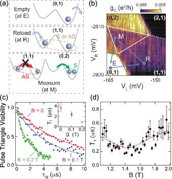
Spin-valley relaxation has been measured in the device of Fig. 3(a,b). This device, fabricated from a 13C nanotube, incorporates a double quantum dot and a nearby charge sensor, coupled via a floating coupling antenna, whose conductance is sensitive to the charge occupancy of the double dot. Relaxation is studied by preparing an two-electron state, Pauli blocked in (1,1), and using the charge sensor to monitor the time to decay to an unblocked state Churchill et al. (2009b).
The two-electron state is manipulated using a cycle of gate voltage pulses applied to gates L and R (Fig. 3(b)), to switch the dot potentials between different configurations (Fig. 36(a,b)). The cycle Johnson et al. (2005) begins with the device configured at point E in gate space, where tunneling to the leads prepares the (0,1) configuration. The device is then pulsed to point R in (1,1), where an electron is reloaded into the left dot. Because is small in the (1,1) configuration (left side of Fig. 29(d)), the two-electron state after reloading can be either or . For readout, the device is quickly pulsed to point M, corresponding to the right side of Fig. 29(d), where the ground-state configuration is . Here a symmetry-to-charge conversion occurs; if the prepared two-electron state was , the left electron will tunnel to the right dot, leading to (0,2) occupancy. However, for states, Pauli blockade enforces occupancy (1,1). This persists for a time , until spin-valley relaxation232323We define spin-valley relaxation as relaxation between an and an state. As discussed in Sec. IV.3.3, this can involve a flip of spin, valley, both, or neither (i.e. dephasing only). causes the state to decay to an state, whereupon the device relaxes to (0,2) occupancy.
The time-average charge sensor conductance is monitored with this pulse cycle applied continually. The duration of the third step is chosen to be much longer than that of the others, so that predominantly reflects the average occupancy at M. For , relaxation of the blocked states is negligible, resulting in a large admixture of (1,1) occupancy and corresponding reduced in the “pulse triangle” region of the stability diagram (Fig. 36(b)). For , this admixture is reduced. By fitting the pulse triangle visibility (defined as the difference between measured and the value expected for (0,2), normalized to unity at ) as a function of , the time can be deduced (Fig. 36(c)).
As a function of magnetic field directed approximately along the nanotube, is observed to decrease initially, consistent with prediction (1) above (Fig. 36(c) inset). However, shows a minimum at T (Fig. 36(d)), where the two states with opposite spin approach each other (as in Fig. 21(d)). This is consistent with prediction (2) above, assuming that during step R an electron is sometimes loaded into a state. Neglecting substrate interaction, the relaxation rate is expected to be proportional to the phonon density of states in the nanotube, giving , where is the energy difference between the two states; taking the proportionality constant as a fit parameter and using the measured field misalignment and for this device to calculate , this prediction is found to be in good agreement with the data Churchill et al. (2009b).
The interference oscillations of prediction (3) have not yet been reported. One reason may be that they are sensitive to the confinement potential. Whereas hard-wall confinement should give rise to sharp interference maxima of due to strongly varying overlap of electron and phonon wave functions with energy, soft confinement typical of few-electron devices is expected to lead to less pronounced maxima Bulaev et al. (2008).
V.2 Hyperfine mixing of spin states
V.2.1 Theory
As well as electron-phonon interaction, a major influence on spin evolution in semiconductors is hyperfine interaction with uncontrolled lattice nuclear spins Hanson et al. (2007). An electron in a quantum dot interacts with all of the nuclei with which its wave function overlaps; this is equivalent to an effective Zeeman field that fluctuates slowly about zero due to nuclear spin diffusion. Approximating an equal overlap with all nuclei in the quantum dot, each root-mean-square component of this field is , where is the hyperfine constant and is the number of nuclei in the dot of which are 13C. As discussed in Sec. IV, the local nature of the hyperfine interaction can cause spin relaxation. Here, we explain that this uncontrolled field also constitutes a major source of spin dephasing Taylor et al. (2007), and its strength can be deduced by measuring .
V.2.2 Experiment
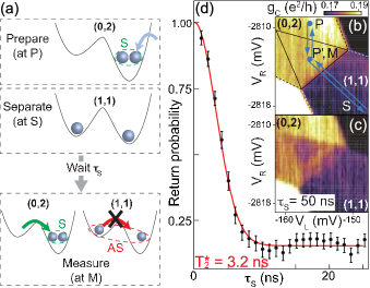
Electron spin dephasing was studied in the same device of Fig. 3(b). This was synthesized using 99% 13C, making hyperfine effects particularly strong. Dephasing was detected through the mixing of and states with the two electrons in separate quantum dots Churchill et al. (2009b). Because the random hyperfine field is in general different between the dots, the separated spins precess at different rates, mixing and states.
The pulse scheme for this experiment (Fig. 37(a-c)) first configures the device in (0,2) at point P, where large causes tunneling to the leads to prepare an state. By tilting the potential into (1,1) (point S, corresponding to left of Fig. 29(d)), the electrons are separated for a time , during which precession in the hyperfine effective field can mix and states. Finally, the gate voltages are pulsed back towards a (0,2) configuration (point M, corresponding to right of Fig. 29(d)) for measurement. As in Fig. 36, states relax to (0,2) occupancy, whereas states remain blocked in (1,1). From the sensor conductance in the measurement configuration, averaged over many cycles, the probability of return to (0,2), and hence the degree of - mixing during the separation step can be deduced Petta et al. (2005).
As a function of , the return probability decays with characteristic time ns (Fig. 37(d)), saturating at a value . Attributing the observed solely to the difference of hyperfine effective field between dots, the effective hyperfine field is given by mT. This is within a factor 2 of the value deduced from Fig. 35 (). However, this apparent agreement again suggests a hyperfine constant two orders of magnitude larger than expected theoretically Yazyev (2008); Fischer et al. (2009).
The long- saturation value of the return probability should reflect the level diagram of Fig. 29(d). Assuming a large longitudinal level spacing, so that only one shell in each dot needs to be considered, the (1,1) configuration allows 16 states, but the lowest manifold in the (0,2) configuration only six. If mixing is fully incoherent, the saturation probability will then be . If mixing is coherent, will generally be higher242424For example, in conventional semiconductors incoherent mixing gives but coherent mixing in a random Overhauser field gives or depending on magnetic field Taylor et al. (2007).. The case of a clean nanotube ( but including spin-orbit coupling) was analyzed by Reynoso and Flensberg (2011), who calculated the value for a range of specific cases. Depending on whether the system is prepared in its ground state, whether passage through the anticrossings in Fig. 29(d) is adiabatic, and depending on the strength of the magnetic field, can be enhanced as high as unity. Including valley mixing makes the situation even more complicated because may differ between the dots. This gives rise to new avoided crossings in the level scheme of Fig. 29(d). The speed at which these crossings are passed, set by the detuning sweep rate, is of critical importance Ribeiro et al. (2013a, b). In the simplest case, where the ground state is always prepared and the first crossing is adiabatic, a value is predicted, with corrections due to non-adiabaticity always positive Reynoso and Flensberg (2012). The measured is therefore lower than all theoretical predictions.
V.3 Qubits
V.3.1 Qubit states and the Bloch sphere
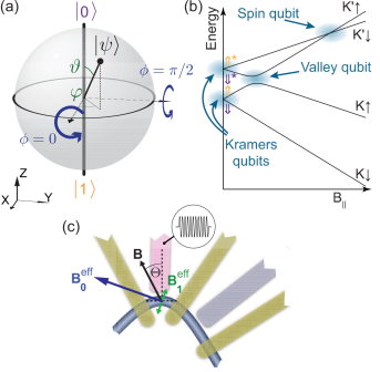
A quantum bit, or qubit, is a two-level system that can be controlled in a quantum coherent way Nielsen and Chuang (2000). An intuitive way to represent the state of a qubit is as a point on the surface of the Bloch sphere (Fig. 38(a)). With two orthogonal states of the qubit (for example two spin states) assigned as the basis states and , any superposition can be written , where the parameters and are polar coordinates representing that state. Any unitary single-qubit operation then corresponds to a rotation about the origin.
How can such rotations be achieved? One technique is by resonant driving at a frequency corresponding to the energy splitting between qubit states Hanson et al. (2007). In the case of a spin qubit with gyromagnetic ratio in static magnetic field , a time-varying field at driving frequency and perpendicular to induces transitions with Rabi frequency . In a reference frame rotating with frequency about the axis, the qubit state then precesses at a rate about an axis in the plane set by the phase of the driving field. One can achieve arbitrary rotations by concatenating bursts with appropriate phases.
V.3.2 Valley, spin and Kramers qubits
This section identifies various two-level subspaces in the spectrum of a generic, spin-orbit coupled carbon nanotube that can serve as qubits, and discusses how they differ in terms of their quantum numbers, ease of operation, and immunity to electrical or magnetic noise. The reason for focussing on these particular subspaces is that the splitting can be made small enough to allow resonant qubit manipulation using microwave fields with frequencies in the range GHz that can readily be generated experimentally.
At low field, either Kramers doublet can be used as a qubit subspace, with the two basis states denoted (for one carrier in the shell) and (for two carriers in the shell) to emphasize the isomorphism with a spin qubit. In a parallel magnetic field and neglecting disorder, these are the eigenstates and , but for general field direction or with disorder, they become entangled states of spin and valley. Experimental manipulation of these qubits, known as Kramers qubits or valley-spin qubits, is described in Sec. V.3.3-V.3.4 Rohling and Burkard (2012). Kramers degeneracy guarantees that by reducing the magnetic field the qubit splitting can be made as small as desired.
Two other qubits can be defined that have not yet been realized experimentally. A pure spin qubit can be defined between the two states that cross at , i.e. and in Fig. 38. For magnetic field aligned with the nanotube, the energy splitting vanishes at the crossing. However, even quite small misalignment leads to an appreciable splitting . For example, with meV and , the minimum driving frequency is GHz. Alternatively a pure valley qubit can be defined at the anticrossing between states of the same spin ( and in Fig. 38). However, the minimum driving frequency, set by , can again be substantial, with a typical experimental value eV leading to minimum GHz. More importantly, it may be difficult to control experimentally.
| Qubit | combined with | ||||
|---|---|---|---|---|---|
| Rashba | Bend | Disorder | Inhom. | ||
| Kramers | |||||
| Spin | |||||
| Valley | 252525if varies on sublattice lengthscale, e.g. from magnetic impurities. | ||||
These various qubits can be manipulated using time-varying electric and magnetic fields. Techniques for driving single-qubit operations have been developed extensively in GaAs quantum dots and many should be applicable to nanotubes Hanson et al. (2007). Several schemes have been proposed. The conceptually simplest is to use an alternating magnetic field as in Sec. V.3.1. This should work for the spin and Kramers qubits, but not for the valley qubit, because it has no magnetic moment in the perpendicular direction. Since time-varying magnetic fields are hard to generate in nanostructures, schemes have been suggested based on time-varying electric fields. The common principle is that moving the electron back and forth leads to an effective magnetic field mediated by spin-orbit coupling. For example, the Rashba-like coupling discussed in Sec. III.6.4 is equivalent to a momentum-dependent perpendicular magnetic field and can be used to manipulate both spin and Kramers qubits Klinovaja et al. (2011a). The corresponding Rabi frequency is however rather low ( MHz), making the driving inefficient in the presence of decoherence. A stronger coupling can be achieved in the presence of a bend, which gives a position-dependent effective magnetic field Flensberg and Marcus (2010) and mediates the only coherent control so far clearly achieved in nanotubes (see next section). Similarly, coupling to a true inhomogeneous magnetic field has been suggested Széchenyi and Pályi (2014). Another proposal relies on inhomogeneity of the disorder parameter . Although random, if this inhomogeneity is static it should allow driving of both Kramers and valley qubits Pályi and Burkard (2011); Széchenyi and Pályi (2014). These possibilities are summarized in Table 5.
As well as the driving mechanism, important considerations are dephasing and decoherence, which limit the coherence time and reduce the fidelity of gate operations. In general, a qubit suffers decoherence through every channel by which it can be driven. As discussed in Sec. V.1-V.2, the dominant decoherence sources in nanotubes are expected to be random time-varying electric fields (e.g. from gate noise and nearby charge switchers) and hyperfine coupling to 13C spins, which acts as an effective time-varying magnetic field on individual lattice sites. The coherence properties depend on the strength and power spectrum of the various noise sources.
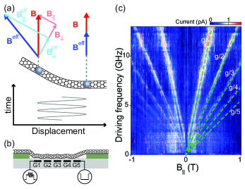
V.3.3 Electrically driven spin resonance in nanotubes
We now focus on the Kramers qubit, which has been experimentally demonstrated. Using bends to mediate qubit control was proposed by Flensberg and Marcus (2010) and realised by Laird et al. (2013). It relies on the anisotropic splitting of the Kramers doublets with magnetic field (Fig 21(d)). Each qubit can be regarded as an effective spin-1/2, with spin vector whose components, just like those of the real spin, have eigenvalues defined as . Unlike the real spin, the Zeeman splitting of this effective spin depends on field angle; the parallel and perpendicular components of the -tensor are:
| (31) | |||||
| (32) |
where upper and lower signs correspond to starred and unstarred doublets respectively. The effective Zeeman Hamiltonian is then:
| (33) |
where is an effective magnetic field, defined as the tensor product , about which precesses. A geometric interpretation of Eq. (33) is shown in Fig. 39(a). When is applied perpendicular to the nanotube (right side of figure), is parallel to . However, when is applied at an angle because the nanotube is bent (left side of figure), the parallel and perpendicular components couple differently, leading to a tilted .
By applying a microwave electric field to a bent nanotube, a quantum dot can be driven back and forth across the bend, experiencing an effective magnetic field that contains both a static component and a perpendicular oscillating component262626Because the confinement energy is usually much larger than the effective Zeeman splitting, to a good approximation the electron experiences the average over the entire dot.. Thus the electric field drives transitions between the two qubit states. Because these two states do not have the same spin, this is a form of electrically driven spin resonance (EDSR).
Detection of EDSR is by measuring the current through a double quantum dot configured in a Pauli-blocked configuration (Fig. 39(c)). With microwaves applied, a peak in current is observed at the resonance condition , indicating spin mixing by EDSR. The measured value presumably arises because this device was highly disordered () and/or in the many-carrier limit, consistent with irregular Coulomb spacings seen in transport data (not shown). As well as the main resonance, a series of subharmonics at integer frequency fractions are seen, due to anharmonicity of the confinement potential or disorder Nowak et al. (2012); Széchenyi and Pályi (2013). The resonant current increases with field as expected from Eq. (33) because and hence becomes larger.
V.3.4 Qubit manipulation and characterization
The data of Fig. 39 shows only state mixing. Quantum coherence is demonstrated by measuring Rabi oscillations Hanson et al. (2007). This was achieved in a less disordered device using a pulsed measurement protocol that shuts off current while microwaves are applied (Fig. 40(a)). The scheme operates near the charge transition, where the qubit states participating in transport are . Gate voltage pulses are used to adjust the detuning between two configurations, one Pauli-blocked where electron tunneling is selective on the qubit state, and one Coulomb-blocked where all tunneling is forbidden Koppens et al. (2006). The sequence has three stages. An initialization stage at a Pauli blockade configuration loads with high probability a parallel two-qubit state, (e.g. ). The device is then configured in Coulomb blockade, where a qubit manipulation microwave burst is applied, possibly flipping one of the qubits. During this step, tunneling is energetically suppressed regardless of the spin state. Finally the configuration is returned to Pauli blockade. If no qubit flip occurred during the manipulation stage, the state remains blocked. However, if a qubit (in either dot) was flipped, tunneling will occur based on the overlap of the electron state on the left with the empty state on the right. Repeating this cycle many times, the time-average current is proportional to the qubit flip probability during the manipulation stage.
As a function of burst duration, this current is observed to oscillate (Fig. 40(b)), indicating coherent rotations between qubit states at Rabi frequency . The fitted is proportional to the driving microwave amplitude (Fig. 40(c)), consistent with a harmonic confinement potential and a smooth bend. The dependence of on field angle is consistent with bend-mediated EDSR coupling Flensberg and Marcus (2010) but not with e.g. Rashba-mediated coupling, suggesting that the bend is indeed the dominant EDSR mechanism in this device.
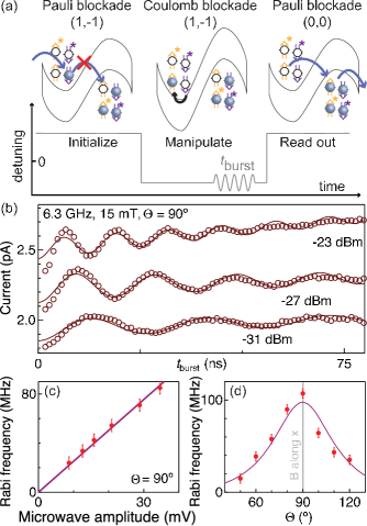
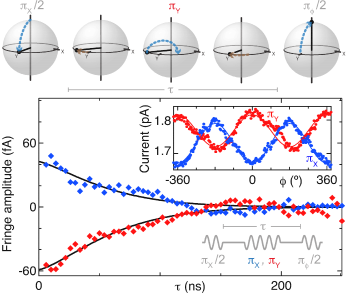
The qubit is characterized further by determining the coherence time Hanson et al. (2007) which characterizes how long a superposition can be preserved by the use of a Hahn echo pulse. The coherence time is measured by a Ramsey fringe experiment (Fig. 41), which consists of (1) a rotation about to create a state on the equator; (2) a wait of duration , with a rotation about or inserted half way; (3) a rotation with phase . Neglecting decoherence, the three rotations interfere to give a qubit flip probability proportional to (Fig. 41 inset). However, for , phase information is lost during the wait step, and the qubit flip probability is 1/2 independent of . By fitting the decay of fringe amplitude versus , the decay time ns is measured (Fig. 41). This coherence time is distinct from the dephasing time discussed in the previous section because the rotation during step (2) makes it insensitive to slow fluctuations of the qubit splitting. The dephasing time of this qubit was measured by a similar method (not shown) and found to be ns Laird et al. (2013).
Both and are quite short compared with some other semiconductor spin qubits, such as GaAs Petta et al. (2005); Greilich et al. (2006); Koppens et al. (2008); Bluhm et al. (2011), Si Maune et al. (2012); Pla et al. (2012), or diamond de Lange et al. (2010), but similar to results in InAs and InSb nanowires Nadj-Perge et al. (2010a); van den Berg et al. (2013). The measured is approximately consistent with hyperfine dephasing, given the unexpectedly large coupling discussed in Sec. V.2.2 Churchill et al. (2009a), but for to be limited in the same way, nuclear spin diffusion would have to be much faster than e.g. in GaAs. This would be surprising, given the one-dimensional geometry and low density of nuclear spins in a nanotube. Fuller consideration of mechanisms led to the tentative conclusion that and perhaps are limited by charge noise Laird et al. (2013). To explain the ineffectiveness of echo at extending the coherence time (even with longer decoupling sequences), this charge noise would need a broad spectral range, in contrast to the spectrum expected for charge switchers in the substrate Cywiński et al. (2012).
V.4 Open questions
Although the main results presented in this section are understood, there are still significant unresolved questions. In all these experiments, it is hard to convincingly identify the precise spin-valley states between which transitions occur. Whereas the experiment of Fig. 36 is sensitive to all forms of relaxation between and states, which may be expected in general to have different rates, a single value appears sufficient to fit each decay curve in Fig. 36(c). Likewise, in the experiment of Fig. 37, it is not clear how the and state populations are redistributed by dephasing, and this is probably reflected in the unexplained value discussed in Sec. V.2.2.
A related mystery comes from the measured EDSR spectra. Although in a disordered many-carrier device, expected resonances with are observed (Fig. 39(c)), the spectrum in a cleaner device is complex and not understood Laird et al. (2013); Li et al. (2014). Whether the unexplained features relate to the short is not known.
An exciting area opened by this work is the possibility to combine the spin degree of freedom with mechanical and optical degrees in clean, suspended nanotubes. There has already been progress in engineering quantized phonons in nanotubes and studying their interactions with the charge on quantum dots Sapmaz et al. (2005a); Sazonova et al. (2004); Lassagne et al. (2009); Steele et al. (2009a); Huttel et al. (2009); Benyamini et al. (2014). Evidence for the discreteness of longitudinal stretching phonon modes, comes from Frank-Condon blockade in suspended nanotubes Sapmaz et al. (2005a); Leturcq et al. (2009), discussed theoretically by Sapmaz et al. (2003); Flensberg (2006); Mariani and von Oppen (2009). By tuning the discrete phonon modes away from resonance with qubit splittings, long qubit lifetimes may be achievable. On the other hand, when the qubit splitting is nearly resonant with a discrete phonon mode, coherent energy exchange should be possible between them, in a solid-state analog of cavity quantum electrodynamics Pályi et al. (2012). Strong spin-phonon coupling in suspended nanotubes may also enable enhanced sensing of nanotube motion Ohm et al. (2012). Finally, Galland and Imamoğlu, 2008; Li and Zhu, 2012 theoretically investigate spin-based mechanics and quantum optics. Using a combination of magnetic fields and optical pumping, they predict high-fidelity all-optical control of electron spins, phonon-induced transparency, and applications in quantum communication.
Finally, we compare this work with the large body of experiments on spin relaxation, dephasing, and diffusion in ensembles of single-walled carbon nanotubes measured via ESR and EDSR spectroscopy at higher temperatures Petit et al. (1997). These techniques focus on resonances that appear within a few percent of at several Tesla. These results seem to contradict the understanding gained from quantum transport experiments because the -factor is expected to be highly anisotropic in clean nanotubes. Therefore the debate whether such resonances reflect intrinsic spin properties of carbon nanotubes Kombarakkaran and Pietraß (2008); Dora et al. (2008), or defects Rice et al. (2013), has yet to be settled. Indeed, sufficiently purified nanotubes where removal of the catalyst was confirmed by TEM were found not to yield an ESR signal Zaka et al. (2010). The level structure of Fig. 21 certainly provides no reason why randomly oriented assemblies of nanotubes should yield resonances at . The only limit where may occur is for samples in which exceeds both and the orbital magnetic field splitting, which is not the case for clean, intrinsic nanotubes.
VI Valley physics in open quantum dots
VI.1 Transport in open regime
Previous sections focused on closed quantum dots where low-transparency barriers ensure that transport occurs by sequential tunneling via strongly confined quantum states. However, nanotube devices with a range of transparencies can be fabricated, allowing the transition from closed to open transport regimes to be studied Nygård and Cobden (2001); Liang et al. (2005); Cao et al. (2005); Grove-Rasmussen et al. (2007). Valley and spin physics again play important roles for highly transmitting devices where the quantum dot states are hybridized with the Fermi seas in the leads. Here we provide an overview of transport mechanisms in open devices and then focus on phenomena involving valley physics: valley and SU(4) Kondo effects (Sec. VI.2) and level renormalization (Sec. VI.3).
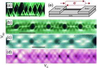
Figure 42(a-d) show transport data from four devices with varying contact transparency. All devices exhibit metallic characteristics at room temperature (not shown) with average conductances ranging from around to , i.e. approaching the maximum conductance of for a single nanotube. The first, low conductance device (a) behaves as a closed quantum dot. For the second device (b) with average , i.e. close to the conductance quantum, the fourfold periodicity due to valley and spin degeneracy leads to clusters of four peaks (Sec. III.4). The enhanced background conductance reflects co-tunneling processes enabled by the stronger coupling. The most extraordinary features are the horizontal (gate independent) ridges of high conductance, e.g. occuring near zero bias in a large fraction of the Coulomb diamonds. These resonances are due to higher order tunneling processes, including Kondo physics, described in the next section.
For the next devices (c-d) the quantum dot features are smeared out as the increased coupling to leads allows for charge fluctuations on the nanotube. However, gate-periodic patterns remain and in the highly transmitting device (d) a distinct pattern of low-conductance lines dominates the spectroscopy plot. Here, in the simplest picture, mode reflections at the contacts (Fig. 42(e)) give rise to interference in transmission, so-called Fabry-Perot resonances Liang et al. (2001). The interference pattern appearing in bias spectroscopy plots is similar to universal conductance fluctuations (UCF) in other mesoscopic systems Ihn (2010); Nazarov and Blanter (2009). However, the randomness that usually characterizes UCF is replaced by nearly perfect periodicity for one-dimensional, ballistic nanotube resonators.
VI.2 Spin, valley and SU(4) Kondo effect in nanotubes
VI.2.1 Theory and background
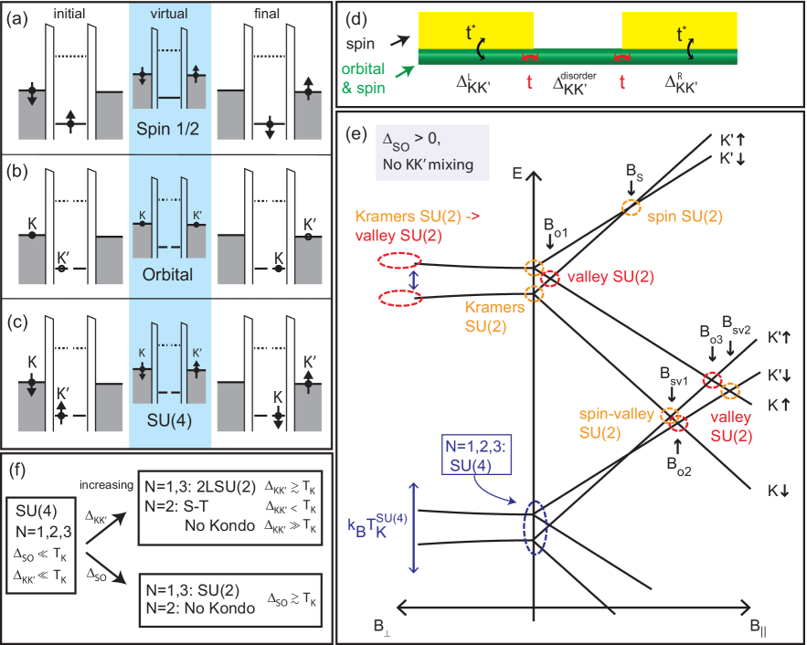
Transport in nearly-closed quantum dots can be described in terms of first-order sequential tunneling. With stronger coupling to the leads higher order processes involving virtual intermediate states become relevant (Fig. 43(a)). Initially, the system is in a state of Coulomb blockade (left). Higher order fluctuations can permit tunneling of the trapped electron to the right lead, while a second electron from the source enters the dot. Effectively, one electron charge, , has been transferred from source to drain (right diagram) via an intermediate state (middle) that is classically forbidden due to energy conservation and Coulomb blockade. Such a process is called elastic co-tunneling Averin and Nazarov (1992); Pustilnik and Glazman (2004); Ihn (2010). In Fig. 43(a) the spin on the dot is flipped as permitted by the spin degeneracy of the level at zero field. The non-trivial result of such higher order spin-flip transitions is the appearance of a new correlated ground state for the combined lead-dot system. This is an effective singlet state between an unpaired spin and the Fermi sea of electrons in the leads. It forms a highly transmitting channel between source and drain at the Fermi energy, known as a Kondo resonance, leading to the breakdown of Coulomb blockade Ihn (2010); Nazarov and Blanter (2009); Heikkila (2013).
The Kondo state only exists at low temperatures where coherence is preserved. The transition temperature from Coulomb blockade to transport resonance is denoted the Kondo temperature, . The energy scale can be considered as the binding energy of the many-body singlet state formed from the quantum dot spin and a screening cloud of electrons in the lead. Kondo resonances appear in Fig. 42(b) as ridges of high conductance near zero bias. The corresponding charge states can be identified as the odd occupancy states where the quantum dot holds an unpaired electron. (The apparent resonances in some of the even diamonds will be discussed below.) Several diagnostics can verify an underlying Kondo mechanism; the resonance should be suppressed by increasing temperature, bias voltage or an external magnetic field that breaks the necessary level degeneracy.
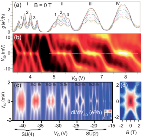
Quantum dot Kondo resonances were first discovered in two-dimensional semiconductor devices Goldhaber-Gordon et al. (1998b); Cronenwett et al. (1998); Simmel et al. (1999) but observed shortly afterwards in carbon nanotubes Nygård et al. (2000); Liang et al. (2002); Buitelaar et al. (2002a); Babić et al. (2004). For a more detailed account of Kondo physics and the relation to quantum dots in general we refer to other reviews Kouwenhoven and Glazman (2001); Pustilnik and Glazman (2004); Grobis et al. (2007); Zaránd (2006) and textbooks, e.g. Ihn (2010); Nazarov and Blanter (2009); Heikkila (2013). In all cases, the spin Kondo effect leads to an enhanced conductance at low temperatures. For nanotubes is typically 1-10 K.
We will not dwell on the details of the spin Kondo effect but rather point out that in principle any doubly (or higher) degenerate localized state with identical quantum numbers in the leads could mediate Kondo-like resonances. The origin of the degeneracy does not need to be spin; for example, transport resonances could be induced by an orbital level degeneracy on the dot (Fig. 43(b)) Jarillo-Herrero et al. (2005b). In the context of nanotubes the valley degree of freedom comes to mind. Below we discuss such a valley Kondo effect.
Both the ordinary spin 1/2 Kondo effect and the two-fold valley Kondo effect reflect SU(2) symmetry. However, for ideal nanotube dots the concomitant existence of valley and spin freedom leading to an approximate four-fold degeneracy could potentially lead to a Kondo effect described by the higher SU(4) symmetry class Choi et al. (2005). This situation is absent in most other quantum dots, which lack the spatial symmetry that naturally leads to valley degeneracy in nanotubes272727SU(4) Kondo physics has been studied in vertical quantum dots Sasaki et al. (2004), parallel double quantum dots Wilhelm et al. (2002); Holleitner et al. (2004); Okazaki et al. (2011); Keller et al. (2013) and single dopants Tettamanzi et al. (2012). In the vertical quantum dots, an orbital degree of freedom also exists in both the leads and the dot because they share similar symmetry. To study SU(4) physics in two parallel dots, however, requires a device with identical intra- and inter Coulomb energy.. Figure 43(c) shows an example of states involved in this scenario where both the valley and spin quantum numbers can be exchanged during co-tunneling. In order to probe the SU(4) Kondo effect, it is essential that transitions between all four states are possible.
Even if valley degeneracy exists in the nanotube, this does not ensure that the valley quantum number is also present in the leads. Figure 43(d) shows a nanotube quantum dot coupled to metallic leads. The double arrows indicate that electrons need to enter a nanotube lead segment () before tunnelling onto the quantum dot () to allow for SU(4) Kondo physics since this effect requires valley-conserving tunneling. As discussed below, - mixing during tunneling (), on the dot (), and in the lead segments () must all be weak, as must spin-orbit coupling.
To link the different Kondo phenomena to the nanotube level structure, the spectrum of two shells is plotted in Fig. 43(e), including spin-orbit interaction but not valley mixing. Dashed ellipses indicate degeneracies that can lead to Kondo physics. When the SU(4) Kondo energy scale is much larger than the spin-orbit splitting, the SU(4) Kondo effect can be observed at zero field for occupations or 3 as depicted for the lower shell. The opposite case of small SU(4) Kondo temperature is shown for the upper shell, resulting in SU(2) Kondo effects for the two split Kramers doublets (dashed circles at zero field) Fang et al. (2008, 2010); Galpin et al. (2010).
Figure 43(e) also points to possible Kondo effects in a parallel magnetic field. Two intra-shell SU(2) Kondo effects are illustrated for the upper shell: a valley SU(2) Kondo effect at half-filling and a spin SU(2) Kondo effect for three electrons in the shell. Inter-shell valley Kondo effects can arise from level crossings between two different shells. Taking account of valley mixing within the shells modifies the energy diagram (Fig. 21), but does not qualitatively change the inter-shell valley degeneracies Jarillo-Herrero et al. (2005b); Grove-Rasmussen et al. (2012). However, the intra-shell valley degeneracies for parallel and perpendicular field are split, and when valley mixing dominates, a spin-orbit split degeneracy (not shown) emerges at finite perpendicular field giving rise to a singlet-triplet (S-T-) Kondo effect Nygård et al. (2000); Pustilnik et al. (2000); Quay et al. (2007). The zero-field SU(4) Kondo effect survives as long as the Kramers doublet splitting due to valley mixing and spin-orbit coupling is much smaller than the Kondo temperature Borda et al. (2003); Galpin et al. (2010); Fang et al. (2008).
As shown in Fig. 43(e-f), the SU(4) Kondo effect can be observed for filling Anders et al. (2008), but only if the valley quantum numbers are conserved during tunneling, i.e. no valley mixing. If this is not the case, the SU(4) Kondo effect reduces to two-level (2L) spin SU(2) Büsser et al. (2011); Büsser and Martins (2007); Choi et al. (2005); Lim et al. (2006) and singlet-triplet (S-T) Izumida et al. (2001); Eto and Nazarov (2000); Sasaki et al. (2000) Kondo effects for and , respectively282828The analysis in terms of singlet-triplet physics assumed zero spin-orbit interaction.. For the 2LSU(2) Kondo effect, the Kondo temperature and maximum conductance at the center of the Coulomb diamond is the same as in the case of SU(4) Kondo effect, and the two effects are therefore to be distinguished either by magnetic field spectroscopy Jarillo-Herrero et al. (2005b); Choi et al. (2005) or by the overall shape of the conductance versus gate voltage Makarovski and Finkelstein (2008). Similarly, in the center of the Coloumb diamond, both the singlet-triplet and SU(4) Kondo effects have the same theoretical maximum conductance Jarillo-Herrero et al. (2005b). However, for sufficiently strong valley mixing (or spin-orbit interaction), a zero-field Kondo effect is absent for , as indicated in Fig. 43(f).
VI.2.2 Experiment
Unconventional Kondo physics in nanotubes was first experimentally studied in Jarillo-Herrero et al. (2005b) and later by Jarillo-Herrero et al. (2005a); Makarovski et al. (2007, 2007); Makarovski and Finkelstein (2008); Cleuziou et al. (2013); Schmid et al. (2015)292929Other types of unconventional Kondo phenomena such as the two-impurity Kondo effect have been studied in nanotube systems Chang and Chen (2009); Chorley et al. (2012); Bomze et al. (2010). Equipping nanotubes with superconducting or ferromagnetic leads also give rise to new Kondo systems Buitelaar et al. (2002b); Hauptmann et al. (2008), beyond the scope of this review.. For all but the last two experiments, the spin-orbit interaction was thought to be negligible and thus not included in the Kondo analysis Choi et al. (2005); Lim et al. (2006); Büsser and Martins (2007); Anders et al. (2008); Mizuno et al. (2009). However, more recent theory includes spin-orbit interaction and reinterprets the early data Fang et al. (2008, 2010); Galpin et al. (2010). Our aim is to present data relevant for the spectrum of Fig. 43(e), starting with zero magnetic field Kondo physics followed by finite field phenomena for one and two shells.
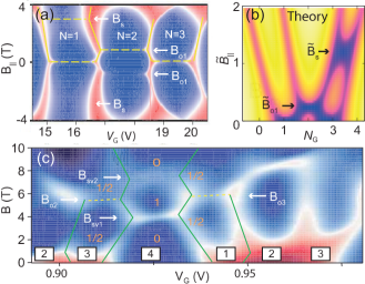
The ideal devices for studying an SU(4) Kondo effect are quantum dots with tunable couplings to the leads. Such devices can be realized in narrow-gap nanotubes where the conductance typically increases as carriers are added. Figure 44(a-b) shows the linear conductance versus gate voltage and the corresponding charge stability diagram. A regular shell structure with zero-bias Kondo ridges for electron filling one, two and three is observed at low gate voltages. At stronger electrode coupling, the different charge states fully hybridize Makarovski et al. (2007); Makarovski and Finkelstein (2008) and a single merged peak is observed for the two rightmost shells in Fig. 44(a). In this mixed-valence regime the lifetime broadening is comparable to or larger than the charging energy and the single-electron transport features of the stability diagram merge into broad ridges. The observed behavior in both the Kondo and mixed-valence regimes has been reproduced by numerical renormalization group (NRG) calculations within an SU(4) Anderson model for various lead couplings, supporting this interpretation Anders et al. (2008).
Figure 44(c) systematically studies the transition from SU(4) to SU(2) Kondo physics in a clean narrow-gap device Cleuziou et al. (2013). The crossover is measured across seven shells, thereby varying both the spin-orbit interaction (decreases with filling, see Fig. 19) and the lead coupling (increases with filling). A transition from to versus hole filling, i.e. SU(2) to SU(4), can thus be realized in accordance with the lower arrow in the flow diagram of Fig. 43(f).
The SU(4) Kondo effect was also reported by Jarillo-Herrero et al. (2005b, a) studying the zero-bias peak. The temperature dependence (0.3 K to 10 K) of the conductance peaks was consistent with the expected empirical scaling formula Goldhaber-Gordon et al. (1998a) yielding high Kondo temperatures (around K). Figure 44(d) shows the behavior of the Kondo resonance in a (parallel) magnetic field. The splitting into four peaks (ideally six if the Zeeman splittings are fully resolved) indicates SU(4) Kondo physics, since only two peaks would emerge if valley mixing induced by tunneling or disorder were dominant as for the 2LSU(2) Kondo effect Choi et al. (2005). A zero-bias ridge observed for in the same work was analyzed in terms of singlet-triplet Kondo physics, but is also consistent with an SU(4) Kondo effect Büsser and Martins (2007).
Next we turn to Kondo phenomena at finite within a single shell (upper part of Fig. 43(e)) Fang et al. (2008, 2010); Galpin et al. (2010). Recent experiments on the addition of the first four electrons in a device with clearly identified spin-orbit interaction give hints of the valley and finite-field spin SU(2) Kondo effects Cleuziou et al. (2013). Figure 45(a) shows the linear conductance versus parallel magnetic field and gate voltage, with the electron filling and the possible Kondo ridges indicated. Compared to the model above, the finite field spin SU(2) Kondo effect at for odd filling appears for instead of . (Whether it is the upper or lower two states that crosses at high field depends on carrier type and the sign of the spin-orbit interaction (see Fig. 18)). The valley Kondo effect at is clearly visible close to the Coulomb peaks, mimicking the behavior of the Kramers Kondo effect at zero field. Due to small tunnel coupling in this device, valley or spin Kondo physics cannot be unambiguously identified from the data.
Similar data with strong Kondo ridges were already observed before the identification of nanotube spin-orbit interaction (see Fig. 12, shell around V), but the Kondo ridge at half filling and finite was interpreted in terms of singlet-triplet Kondo physics303030Depending on the exchange interaction, the triplet state occupying two different valleys may become the ground state. In a parallel magnetic field the singlet state occupying two down-moving valleys thus crosses the almost degenerate triplet states, giving rise to a Kondo effect (assuming negligible Zeeman effect). Jarillo-Herrero et al. (2005a). Later NRG modelling (Fig. 45(b)) suggested that the data could also be explained in terms of the spin-orbit energy spectrum313131While this is a likely interpretation, some caution should be applied since level crossings with a different shell complicate the finite-field spin SU(2) identification. Galpin et al. (2010). The calculated color plot thus represents the ideal Kondo behavior for the upper shell in Fig. 43(e). Other experiments with dominating valley mixing () also identify the spin SU(2) Kondo effect at Jespersen et al. (2011b); Schmid et al. (2015).
Finally we address the (inter-shell) valley Kondo effect. It can be found at particular fields () that induce valley degeneracy but not spin degeneracy (Fig. 43(e)). Figure 45(c) shows the (parallel) magnetic field evolution of the conductance for a nanotube quantum dot that has strong Kondo resonances at zero field. At finite fields additional resonances appear at and , consistent with valley degeneracies inducing a spinless valley SU(2) Kondo effect. The appearance of this Kondo resonance indicates that tunneling preserves the valley symmetry, which for this device is less obvious because of the metal deposited on top of the nanotube leads.
In several of the experiments above a Kondo effect arising from inelastic transitions gave rise to conductance peaks at finite bias. Such Kondo enhancement of inelastic cotunneling thresholds was observed and modelled in Paaske et al. (2006) while a recent experiment revealed that certain cotunneling thresholds are not observed in the strong coupling regime Schmid et al. (2015). The authors identify the two states involved in the relevant cotunneling processes as particle-hole symmetric323232The work considers a shell with both spin-orbit interaction and valley mixing. The eigenstates are therefore superpositions of all four basis states . A simple example of a particle-hole symmetric pair is {}. and show theoretically that these processes do not give rise to Kondo correlations (even though cotunneling is allowed).
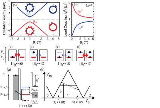
VI.3 Level renormalization
The most visible consequence of increasing electrode couplings in Fig. 42 is a broadening of the energy levels, but this hybridization is also accompanied by level shifts. These shifts are named tunnel renormalization, since the effect stems from quantum charge fluctuations (cotunneling events) that are particularly relevant when the tunnel couplings are large. Nanotube quantum dots have turned out to be ideal to observe such level shifts, in particular when the two doublets are differently coupled to the leads Holm et al. (2008).
VI.3.1 Theory
We consider a spinless nanotube shell model without any internal couplings and assume metallic leads (no valley quantum number). Since and states are time-reversed partners, the tunnel couplings are equal Introducing a complex valley mixing term results in new eigenstates which have phase dependent tunnel couplings Grove-Rasmussen et al. (2012). Figure 46(a) shows the energy versus parallel magnetic field for the new eigenstates that arise when the valley states are coupled. The schematic insets show that the electron probability distributions for the two eigenstates are different at zero field and thus the tunneling amplitude may be different depending on the exact site of a microscopic contact. This picture of tunneling into one particular atomic site with different probability for the two wave functions is probably too simple for a real device but is adopted here as a minimal model. In Fig. 46(b) the lead couplings for the two states are plotted for the case . At zero field the two new eigenstates have different couplings: the ground state doubles its coupling to the leads compared to the original states while the excited state decouples. The model also makes an important prediction about the magnetic field dependence of the couplings. At high parallel magnetic fields the ground and excited state couplings become equal, since the eigenstates are close to the original valley states and whose probability distributions are equal at high fields (Fig. 46(a) inset).
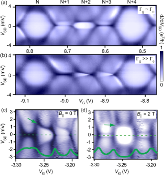
We now examine the effect of the difference in lead-couplings on cotunneling. Consider two states with different tunnel couplings as shown in Fig. 46(c-d) for a singly occupied dot . The ground state experiences stronger cotunneling charge fluctuations via the zero state () than the excited state does () does. The renormalization shift increases with the coupling of the levels and thus the more strongly coupled state has the larger energy shift (Fig. 46(g)). Consequently, the threshold for inelastic cotunneling transport will increase (from to ) near the charge transition (left side of diamond). In the stability diagram Fig. 46(h) the threshold will correspondingly be shifted to higher bias. In contrast, on the right side of the one-electron diamond, the dominant cotunneling processes involve the two-electron state (). The situation is opposite here since the excited state experiences stronger fluctuations and level shifts than the ground state (Fig. 46(e-f)). Thus the cotunneling threshold will be reduced compared to the original level in this gate range. The resulting stability diagram is sketched in Fig. 46(h). The models above are easily extended to include spin and higher fillings, but the conclusions remain the same: tunneling-induced level renormalization can result in gate-dependent cotunneling features within the charge stability diamonds.
VI.3.2 Experiment
Figure 47(a) shows a stability diagram with shell filling identified by the characteristic pattern of three small Coulomb diamonds followed by a large one and Kondo ridges for odd occupancies. However, Fig. 47(b) shows that this regular behavior is, not observed for all shells. In this case, the Kondo effect is only evident for one electron, and the inelastic cotunneling thresholds333333For the one-electron case the inelastic cotunneling threshold is not visible due to the Kondo effect present at zero bias. are seen to have a marked gate dependence for two and three electrons where arguments similar to the model above hold (compare Fig. 46(h)). The absence of the Kondo effect for indicates that the ground-state doublet is more strongly coupled to the leads than the excited-state doublet. The different behavior for different shells, such as between Fig. 47(a) and (b), can be understood as due to valley mixing with different phases for each shell and tunnel renormalization.
The effective doublet splitting is set by both spin-orbit and valley coupling, , while in the lead-coupling model of Fig. 46(b) the origin of the coupling asymmetry was the valley coupling alone. The validity of this model can be tested by examining its prediction for the lead tunnel couplings in a magnetic field. Figure 47(c) shows a stability diagram of a shell whose behavior is similar () to that of Fig. 47(b). The corresponding stability diagram in parallel magnetic field T is shown in Fig. 47(d). As predicted qualitatively by the model, the gate dependence of the cotunneling threshold disappears at large field where the lead couplings become equal, consistent with the observed widths of the Coulomb peaks within the shell (see cut in Fig. 47d). This observation indicates that the origin of the asymmetry is related to valley mixing Grove-Rasmussen et al. (2012).
Renormalization effects have also been established in devices with ferromagnetic leads, where the difference in spin density of states of the electrodes leads to different effective tunnel coupling Martinek et al. (2003, 2005); Pasupathy et al. (2004); Hauptmann et al. (2008). Furthermore, if valley mixing originates from cotunneling (not only disorder as described above) different gate-dependent shifts are predicted with the possibility of inelastic cotunneling lines crossing inside the Coulomb diamond Kiršanskas et al. (2012).
VI.4 Open questions
Several experiments have found features consistent with Kondo correlations originating from the additional valley degree of freedom. A complete study of the SU(4) Kondo effect would, however, call for control of the valley mixing parameters (Fig. 43(d)), to tune the valley Kondo correlations. Valley mixing also plays a role for the inter-shell valley Kondo experiment, where incipient Kondo correlations enhancing finite bias features are analyzed Jarillo-Herrero et al. (2005b); Paaske et al. (2006). Such correlations are generally more difficult to quantify. Clearer experimental results may be possible in tunable gate-defined dots with weak valley mixing, where the leads are nanotube segments rather than metal.
VII Correlated-electron effects
VII.1 Introduction
Electron correlation effects due to Coulomb interaction can be strong in carbon nanotubes. One reason is the one-dimensional nature of the confinement: electrons in two or three dimensions can minimize their Coulomb repulsion by moving out of each other’s way. Electrons in nanotubes do not have this freedom, and instead tend to develop strong correlations. Electrons in nanotubes also see an environment with a low dielectric constant, which for suspended nanotubes approaches the free-space value . This is in contrast to electrons in semiconductors, where electric fields can be screened by the large dielectric constant of the host material. These properties suggest that nanotubes are an interesting system for studying electron correlations.
The strength of Coulomb interactions between particles with parabolic dispersion is characterized by an interaction parameter , defined as the ratio of the average interparticle spacing to the Bohr radius :
| (34) |
Within a numerical constant of order unity, is also the ratio of the Coulomb interaction energy to the kinetic energy . At high densities (small ), kinetic energy dominates and the single-particle approximation can be used for the electronic states. At low densities (large ), kinetic energy is quenched and the Coulomb interaction dominates the physics.
For semiconducting nanotubes at sufficiently low densities, the Fermi energy lies in the parabolic region of the dispersion relation (cf. Fig. 5) and is a useful characterization of the strength of electron interactions. A typical Coulomb interaction energy in a nanotube for and nm is meV. To estimate the kinetic energy, it is important to note that the effective mass is strongly dependent on the bandgap. For a semiconducting nanotube with a bandgap of 210 meV (), eV (Bohr radius nm). This implies that two electrons in a 200 nm long quantum dot in such a nanotube corresponds to very strong interactions ()343434Taking electrons..
Advances in making clean suspended nanotubes have enabled the study of quantum dots at very low density with very low electronic disorder. Using these new devices, the question of electron interaction and correlation effects in nanotubes is being revisited from the ground up. In the few-electron regime in the clean limit, a clear understanding of the simplest case of two electrons is beginning to emerge.
VII.2 Interactions in two-electron nanotube quantum dots
The Coulomb interaction does not directly exert a force between spins. For example, spin-spin exchange coupling does not arise from a direct interaction between spins, but instead from a combination of the Pauli exclusion principle with the Coulomb repulsion between orbital wave functions. Thus, to approach Coulomb interaction phenomena, it is important to start by considering the properties of nanotube electronic wave functions.
The spatial wave function in a nanotube has several degrees of freedom: the position along the nanotube axis353535For simplicity, in this section we use notation for the longitudinal coordinate instead of as used elsewhere in the review., a subband index from the quantization around the circumference, and a valley index specifying which of the two valleys () is occupied by an electron. In nanotubes, it is convenient to separate the Coulomb interaction into long-range and short-range components. A natural length scale for this separation is the nanotube diameter. This separation simplifies considerably the treatment of the Coulomb interaction in nanotubes Wunsch (2009). A first approximation is that neither the short-range nor long-range component mixes states from different subbands: this is justified by the large subband spacing, on the order of eV. A second approximation is that only the short-range component of the Coulomb interaction mixes states from different valleys: this is justified since intervalley scattering requires a large momentum shift Mayrhofer and Grifoni (2008); Wunsch (2009); Weiss et al. (2010); Secchi and Rontani (2013). The third approximation is that the envelope function describing the position of the electron along the nanotube axis is independent of spin and valley. Although this is not true in general (cf. Appendix B.6), it is a reasonable approximation for smooth confinement potentials and large quantum dots Wunsch (2009). Within these approximations, we can treat the long-range and short-range components of the Coulomb interaction separately: the long-range component couples to , while the short-range component couples to the valley degree of freedom.
Indications of Wigner correlations in multi-hole quantum dots were identified already in early works Deshpande and Bockrath (2008). In this review, we follow a pedagogical approach to the topic. We start with long-range interactions, presenting a pedagogical model for the Wigner molecule in one dimension, reviewing calculations performed for nanotubes, and discussing experimental results demonstrating a two-electron Wigner molecule. We then focus on effects from the short-range interaction. At the end of the section, we give an outlook towards interactions in the many-electron and many-hole regimes.
VII.2.1 Long-range interactions and Wigner molecules
Our simple model focusses on the spatial two-electron wave function, assuming that antisymmetry of the total wave function is provided by appropriate symmetries in the spin/valley degree of freedom. Approximating the dispersion relation of a semiconducting nanotube by a parabola, we can write down a Schrödinger equation with an effective mass :
| (35) |
where is the two-electron spatial wave function, the external confining potential, and the Coulomb interaction between electrons. To restrict ourselves to the long-range component of , we include a cutoff in the Coulomb potential as follows:
| (36) |
with is chosen as the nanotube diameter. It is instructive to combine the confinement terms in a two-electron electrostatic potential . The problem of two interacting electrons in one dimension is then formally equivalent to that of a single electron confined in a two-dimensional potential .
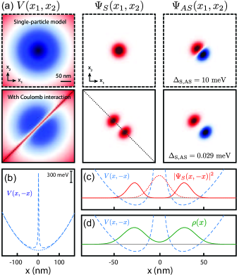
This problem can be solved on a desktop computer by exact diagonalization Jauregui et al. (1993); Szafran et al. (2004); Balder (2008). The results are shown in Fig. 48, taking , (corresponding to meV and nm) and with meV (confinement length 30 nm). These parameters correspond to Balder (2008). The results with () and without () Coulomb interaction are shown in Fig. 48(a). Including interactions (lower panels in (a)), the Coulomb repulsion can be seen in as a diagonal line along . With these parameters, typical for nanotubes, the Coulomb interaction dominates over the confinement potential. In response, the single lobe of in the single-particle model splits into two well-separated lobes, pushing the two electrons away from each other to minimize Coulomb repulsion (Fig. 48(c,d)). In this state, the two-electron probability density goes rapidly to zero along the line, indicating the formation of a Wigner molecule. The quantity in Fig. 48(c) can be viewed as a two-particle correlation density363636Integrating along the diagonal in Fig. 48(a) yields the two-particle correlation function ., and its suppression near corresponds to the formation of a “correlation hole” (Fig. 48c).
An important property of the Wigner molecule state is a strong suppression of the splitting between the spatially symmetric ground state and the spatially antisymmetric excited state . Without interactions, meV, where is the single-particle level spacing. Including interactions, the splitting drops dramatically to eV, smaller by a factor . An explanation can be seen by plotting the two-electron wave functions (lower panels of Fig. 48(a)). In the Wigner molecule regime, the ground state wave function deforms to minimize the Coulomb energy, gaining kinetic energy and reducing until the symmetric ground state and antisymmetric excited state are nearly degenerate.
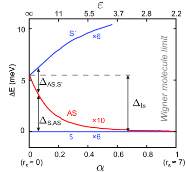
Until now, the discussion has been quite general and applies equally to other one-dimensional systems. The relevance for carbon nanotubes becomes clear when looking at the magnitude of such effects. Exact diagonalization calculations for nanotubes Wunsch (2009); Secchi and Rontani (2009, 2010, 2012, 2013); Roy and Maksym (2009, 2012) arrive at the same conclusions as our toy model: the two-electron dot is strongly correlated, forming a Wigner molecule. The results of such a calculation are shown in Fig. 49. The input parameters are a 100 nm square-well confinement potential with a 50 meV barrier height, a nanotube diameter of 5 nm, a bandgap of 90 meV, and an effective mass of . To illustrate the transition from the single-particle limit to the Wigner molecule limit, the strength of the Coulomb interaction is tuned by changing the environmental dielectric constant , parametrized by an effective fine structure constant (so that ). With no long-range interactions (), the excited multiplet is 16-fold degenerate () and separated from the ground-state multiplet by the single-particle level spacing (). With strong interactions (), the antisymmetric multiplet is pushed down in energy relative to the ground state, with becoming exponentially small. The two-electron state is deep in the Wigner molecule limit for , and already strongly correlated for intermediate . Summarizing these predictions, Wigner correlations in a two-electron quantum dot cause a collapse of .
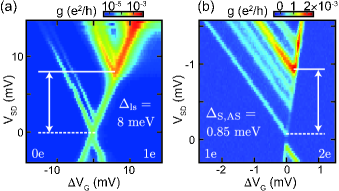
Experiments with clean nanotubes have provided clear evidence of a Wigner molecule. Specifically, Pecker et. al (2013) compared a one-electron to a two-electron quantum dot in the same device (Fig. 50). A crucial step was a careful analysis of the magnetic field dependence of the excitation lines (Fig. 31). This allowed the authors to determine which splitting in Fig. 50(a) corresponds to , and which splitting in Fig. 50(b) corresponds to . They found meV and meV. The 10-fold suppression of compared to indicates that the two-electron quantum dot indeed forms a Wigner molecule.
VII.2.2 Short-range interactions and intervalley exchange
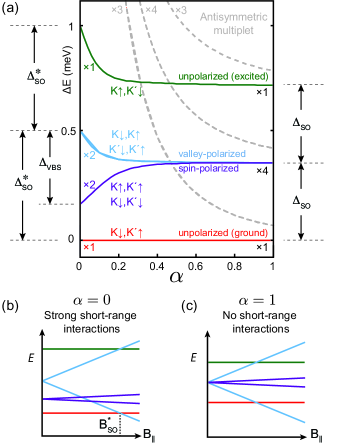
In this section, we consider effects of the short-range Coulomb interaction on the spectrum of a two-electron quantum dot. As seen in the toy model, the long-range interaction distorts the longitudinal wave functions, reducing the splitting between the symmetric and antisymmetric multiplets. Because the long-range interaction does not couple to valleys, it does not change the spin/valley level structure inside a multiplet. In contrast, the short-range Coulomb interaction can induce valley scattering, and thus changes the splitting between different valley and spin states.
Several exact diagonalization calculations have been performed accounting for Wigner molecule effects, spin-orbit coupling, and short-range Coulomb interactions Wunsch (2009); Secchi and Rontani (2009, 2010, 2012, 2013). The resulting spectrum is shown in Fig. 51. In the calculation, is set to zero to artificially suppress long-range interactions while keeping the short-range on-site energy373737The Coulomb potential for the short-range interaction is taken with the same form as Eq. (36), but with cutoff chosen such than , where eV is the charging energy associated with putting two electrons on the same orbital. Such a potential is also referred to as the Ohno potential Mayrhofer and Grifoni (2008). constant383838Physically, this could be achieved by placing the nanotube close to a metallic gate or dielectric slab, such that the distance to the surface is large compared to the diameter but small compared to the nanotube length.. Figure 51(a) shows the spectrum as a function of at zero magnetic field. The colored (grey) lines represent the () multiplet of Fig. 49. For , the dot is in the Wigner molecule regime due to long-range interactions, and the grey lines in (a) become nearly degenerate with the colored lines. Panels (b) and (c) show the dependence of the spatially symmetric multiplet for and .
The influence of short-range interactions can be most clearly seen for (Fig. 51(b)). The first effect is to lift the degeneracy of the spin-polarized and valley-polarized states. In the single-particle model (and also at , see below), these four states are degenerate at . With strong short-range interactions, the energy of the valley-polarized doublet is raised with respect to the spin-polarized doublet. This is because a positive used in the calculation penalizes double occupancy of atomic sites, which by symmetry considerations does not occur for spin-polarized states (see Appendix B.9 for details). This results in a new splitting within the multiplet, which can be viewed as an effective intervalley exchange energy393939Note that Fig. 51 plots the energies with respect to the ground state, explaining why spin-polarized states appear to be lowered with respect to valley-polarized states. The abbreviation VBS denotes “valley backscattering”, a name used for the term in the Coulomb scattering matrix that gives rise to an intervalley exchange splitting.. For the multiplet, the effect of short-range Coulomb interaction is predicted to be much smaller Secchi and Rontani (2013), indicating that the longitudinal symmetry of the two-electron wave function plays an important role (Appendix B.9).
The second effect of the short-range interaction is seen in Fig. 51 as an increase in the splitting between the unpolarized ground state and the unpolarized excited state. The splitting is now equal to instead of . An important consequence is that the two-electron ground state becomes valley-polarized at a higher magnetic field than without short-range interactions (the crossing field is higher in (b) than in (c)). In the Wigner molecule regime () the effects of short-range interactions are suppressed: Due to strong correlations, the two electrons have little overlap irrespective of their longitudinal symmetry, thereby suppressing double occupancy of the same atomic site. Similar intervalley exchange effects have also been seen in other calculations Mayrhofer and Grifoni (2008); von Stecher et al. (2010); Secchi and Rontani (2009, 2010, 2012, 2013).
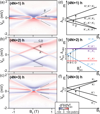
Experiments by Cleuziou et al. demonstrated clear intervalley exchange effects in the spectra of clean nanotubes in the many-hole regime (Fig. 52). The key observation was that the and charge states showed a spectrum consistent with shell-filling of the single-particle valley/spin levels, whereas a different spectrum was observed for the charge state Cleuziou et al. (2013). This difference between odd and even filling of the nanotube multiplet is a clear signature that can only be explained including short-range interactions.
The spectrum measured for filling is similar to that of Fig. 51(b), except for the sign of the exchange interaction. In particular, theoretical treatments of intervalley exchange as outlined above predict that the valley-polarized states are raised in energy above the spin-polarized states (as in Fig. 51(b)). In contrast, the observed spectra Cleuziou et al. (2013) show the opposite (Fig. 52(e)). This may indicate that the exchange integral implied from the experimental data has the opposite sign compared to that predicted by theory so far. A similar observation was also reported for electrons Pecker et al. (2013). The reason for this sign difference is not understood, but suggests that the validity of theoretical approximations, as well as alternative mechanisms, should carefully be checked.
As discussed above, intervalley exchange is not expected to play a significant role in the few-electron regime, since the long-range Wigner correlations will suppress short-range Coulomb interactions. The device of Fig. 52 was in the many-hole regime: a possible explanation of why is so large is that the long-range Coulomb interaction was screened by the holes in nearby shells. However, a large was also reported in the few-electron regime by both Pecker et al., 2013 ( meV) and Cleuziou et al., 2013 ( meV calculated from the observed ). Estimates for uncorrelated states based on first-order perturbation theory predict to be hundreds of eV (Appendix B.7). Taking into account correlations predicts a much smaller value, eV Wunsch (2009); Secchi and Rontani (2009, 2010, 2012); Pecker et al. (2013); Secchi and Rontani (2013). It is an open question why is so large in these experiments.
Finally, the large splitting seen in excited-state spectroscopy has important implications for ground-state spectroscopy, in which the magnetic field dependence of Coulomb peak position in gate voltage is used to infer the spin-orbit splitting Churchill et al. (2009b); Steele et al. (2013). In particular, the magnetic field where kinks occur in the ground-state chemical potentials is now given by instead of by . This raises the possibility that the large spin-orbit interaction reported in Steele et al. (2013) extracted from the ground state energies could be due to a large and instead of a large . The intervalley exchange splitting required to match the experimental data, however, would be meV, even larger than the already unexpectedly large values reported from excitation spectra Pecker et al. (2013); Cleuziou et al. (2013).
VII.3 Beyond Wigner molecules: Correlation effects of many electrons in quantum dots
The search for strong correlation effects with many electrons inspired some of the very first experiments on nanotubes. These early experiments were motivated by the predictions of Luttinger liquid theory Luttinger (1963); Imambekov et al. (2012) and focused on power-law behavior of the conductance Bockrath et al. (1999); Yao et al. (1999). Detailed understanding of these experiments was hampered, however, by the large disorder present in these devices, leading to localization and Coulomb blockade at low temperatures. Dynamical Coulomb blockade also leads to power-law dependence on bias and temperature Ingold and Nazarov (1992). A clearer signature for a Luttinger liquid would be spin-charge separation, giving spin and charge modes with different velocities. Evidence for such spin-charge separation has been seen in GaAs wires Auslaender et al. (2005), but has not been reported for nanotubes.
Correlation effects for two electrons in a carbon nanotube quantum dot are now fairly well understood theoretically, and well established experimentally. A natural question is then: what happens if more electrons or holes are added to the quantum dot? One route could be to probe the electron density itself in the quantum dot using an STM Ziani et al. (2013). Another route is detailed spectroscopy of suspended nanotube quantum dots in the multi-electron and mult-ihole regime. From an experimental point of view, there have been suggestions of correlation effects in clean many-hole quantum dots Deshpande and Bockrath (2008). Studying the ground-state spin and valley filling of a quantum dot as a function of hole number and magnetic field, regions of strong spin and valley polarization were observed that are not easily explained by a single-particle picture. A possible explanation of this strong spin and valley polarization is the formation of a many-hole Wigner crystal in which the kinetic energy is quenched by interactions, similar to the suppressed in the two-electron Wigner molecule. An exciting next step will be to use low-disorder nanotubes with multiple gates to perform detailed spectroscopy with tunable confinement, exploring the transition from the well-established two-electron Wigner molecule to the regime where many-electron Wigner crystals and Luttinger-liquid like correlations may occur.
VII.4 Open Questions
-
•
Why is the observed intervalley exchange splitting so large? Even with a completely screened long-range interaction, calculations predict , while the opposite has been observed in some experiments.
-
•
Why does have the wrong sign in experiments? A possible scenario is a superexchange mechanism for the short-range interaction. In superexchange, a net exchange of two electrons is achieved by two separate exchange processes with electrons in a third orbital. The third orbital could correspond to a state in a different shell, a state in the valence band, or a state in one of the higher subbands. Superexchange can have the opposite sign compared to direct exchange.
-
•
Why are not more devices deep in the Wigner molecule limit? Why is shell-filling theory so effective for describing so many devices?
-
•
Are there qualitatively new predictions from theories that take into account the dependence of the spatial wave function on , , and magnetic field (see Appendix B.6)?
-
•
How do the well-understood strong correlations of the two-electron Wigner molecule extend to quantum dots with more electrons? Are there clear experimental signatures to look for?
VIII Conclusions and Outlook
The chirality is an unknown parameter in all the experiments discussed in this review. Although optical techniques have been developed to determine chirality on specially made, long nanotubes Liu et al. (2013); Amer et al. (2013), these characterizations are unfortunately incompatible with the short length of nanotube devices in the quantum regime. Therefore the growth of chirality-specific nanotubes remains an important challenge, although its realization may not be expected soon. Of course, several important (band-)structure parameters can be inferred from transport, such as the gap and the diameter. Uncertainties nevertheless arise since a measured gap may be affected by electron-electron interactions, or even mundane issues like surface coverage with water Elias et al. (2009). Such band-gap modifications are interesting subjects by themselves but then knowledge of the bare band gap, and thus the chirality, would be an indispensable input parameter.
Fortunately, the general physics discussed in this review does not depend on the precise numerical values of the band-structure parameters. Most of this physics is a consequence of the simple fact that electrons in nanotubes live on a hexagonal lattice that is confined to a one dimensional, tubular geometry. We stress that in this sense nanotubes are unique solid-state structures. Given this structure the spin and valley phenomena described in this review represent general physics independent of the precise chirality.
The inclusion of spin-orbit interaction completes our picture of the non-interacting, single-particle physics in nanotubes. Until 2008, this effect was widely thought to be negligible, but it has turned out to be highly relevant in many experiments. It is also important for applications involving coherent control of quantum states. The emerging picture of the role of interactions has also become much clearer in recent years since ultraclean devices have become available. We have described in detail the case of two interacting electrons. The study of many interacting electrons Deshpande and Bockrath (2008) is a quest full of interesting challenges with its holy grail being formation of a long Wigner crystal.
The theoretical understanding of the single-particle physics has been important to obtain a complete picture of the allowed spin-orbit terms. There are still theoretical challenges relating to a quantitative microscopic understanding of the effects originating from the cylindrical geometry. As part of this, renormalization by long-range Coulomb interactions of the curvature-induced gap and the spin-orbit coupling has not been investigated.
Quantum states are best defined in closed systems and this review has therefore mainly focussed on quantum dots whose coupling to leads is weak (but large enough to allow a measurable current). Quantum dot states change when the coupling is increased, and qualitatively new phenomena can arise such as various Kondo effects and possibly even quantum phase transitions Mebrahtu et al. (2012). Great potential for new experiments arises when the leads are given interesting properties. For example superconducting leads can induce superconducting correlations that are restricted by the special spin-valley quantum numbers of nanotubes. One can imagine Josephson junctions with the junction consisting of a nanotube with multiple bends. Experiments using superconducting contacts performed so far indeed indicate a rich research direction de Franceschi et al. (2010). Also in such hybrid nanotube devices, spin-orbit interactions may play a role, e.g. leading to modified Josephson currents Lim et al. (2011) or new detection schemes Braunecker et al. (2013). Superconducting contacts to ultraclean nanotubes have also recently been demonstrated Schneider et al. (2012), opening the possibility of studying proximity-induced superconductivity with exceptionally low electronic disorder. Magnetic materials could be used as contacts to explore spintronics confined to one dimension Sahoo et al. (2005).
The field of quantum computing has been inspirational for the development of all kinds of qubit devices. This review discussed various types of nanotube. The coherent evolution in qubits can be used as an extremely sensitive probe of the environment. Nanotube qubits could be used to study in detail nuclear spins or mechanical vibrations. The holy grail here could be the realization of a coherent coupling between spin and motion. Another inspiration from the field of qubits is the use of nanotubes as on-chip charge sensors Biercuk et al. (2006); Gotz et al. (2008); Churchill et al. (2009a), or as a component in circuit quantum electrodynamics Delbecq et al. (2011). If long coherence times could be achieved, there is potential for a dramatically improved charge sensor Dial et al. (2013). Nanotubes have the advantage for sensing that short quantum dots show Coulomb blockade up to room temperature Postma et al. (2001).
We hope this review inspires new generations of experiments taking advantage of the unique properties of carbon nanotubes. Similar to the evolution of quantum Hall physics in GaAs in the 1980s and 1990s, the remarkable quality of devices that can now be achieved using ultraclean techniques indicates that nanotubes will remain an exciting playground for exploring rich new physics for years to come.
IX Acknowledgements
We acknowledge many colleagues and collaborators, especially from Delft, Copenhagen, Harvard, Cornell, and Oxford. Especially we thank Ramon Aguado, Hugh Churchill, Thomas Sand Jespersen, Charles Marcus, Jens Paaske, Fei Pei, Emmanuel Rashba, Mark Rudner, Christoph Strunk, Stephan Weiss, and Floris Zwanenburg. We acknowledge support from the Carlsberg Foundation, the Danish Council for Independent Research, the Danish National Research Foundation, the Dutch National Science Foundation, NWO/FOM, the European Union, and the Royal Academy of Engineering.
Appendix A Transport spectroscopy in quantum dots
Here we give a basic overview of quantum dots and transport spectroscopy, focusing on techniques by which data in this review is derived.

A.1 Coulomb blockade and the constant interaction model
An electrical schematic of a quantum dot as in Fig. 2 is shown in Fig. 53. If both the tunnel rates to the leads and the thermal energy are less than the charging energy , where is the total dot capacitance to the outside world, then the electron occupation becomes constrained to take an integer value. The equilibrium occupation can be adjusted by tuning .
This quantization of the dot occupation strongly modifies the transport characteristics of this circuit. With all other parameters held fixed, any change of the dot occupation away from equilibrium increases the electrostatic energy of the system. This causes a suppression of the current known as Coulomb blockade. However, for particular values of , the suppression can be lifted. This allows the energy levels of the quantum dot to be mapped out by measuring the device conductance as a function of (for extensive reviews, see Kouwenhoven et al. (1997, 2001); Hanson et al. (2007))
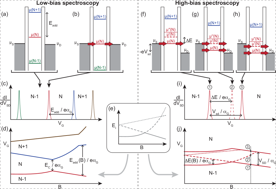
Coulomb blockade is lifted whenever each step of electron tunneling through the device is energetically favourable. To understand how the observed conductance features relate to the energy levels of the device, we introduce the electrochemical potential of the dot for occupation , defined as the difference in energy between -electron and -electron ground states:
| (37) |
Correspondingly, the electrochemical potentials of the leads are defined as the energy to add an additional electron at the Fermi level; with a bias applied to the source as in Fig. 2(a),
| (38) | |||||
| (39) |
where is the Fermi energy.
The electrochemical potential is in general related in a complicated way to the single-particle energy levels, because each electron added electrostatically perturbs the energies of the electrons already on the dot. However, the relationship becomes simpler in the constant-interaction model, which makes two assumptions. First, all Coulomb interactions, both between electrons on the dot and between the dot and the environment, are parameterised by a single constant capacitance , which is the sum of capacitances to the source, drain and gate404040In devices with more than one gate, additional capacitances must be added to the model in a straightforward way.. Second, the single-particle energy levels are assumed to be independent of these interactions, and therefore not changed by adding additional electrons. Under these assumptions, the dot energy is:
| (40) |
where is the occupancy with no voltages applied (set by fixed charges in the environment, e.g. substrate charges, and not necessarily quantized) and are the single-particle energy levels. The first term is the electrostatic energy stored in the dot capacitances, while the second is the sum of the single-particle confinement energies.
In this approximation, the electrochemical potential is:
| (41) |
where is the charging energy. The electrochemical potential increases for successive values of , forming a ladder of levels as shown in Fig. 54. The separation between adjacent levels is the addition energy:
| (42) | |||||
and includes both an electrostatic term and the quantum energy level spacing . From Eq. (41), changing the gate voltage moves the entire ladder of electrochemical potentials up or down.
A.2 Low-bias spectroscopy
The condition that both tunneling events be energetically favourable is equivalent to saying that the chemical potential must decrease at each step414141Thermal excitations in the leads relax this constraint, broadening the Coulomb peaks. Here this effect is ignored, which is permissible if the temperature is less than both and .. In other words, some must exist for which:
| (43) |
Consider first the situation of low bias, where . The corresponding level diagram in the blockaded case (Fig. 54(a)), shows that no ground-state chemical potential satisfies Eq. (43), so no current flows. However, by increasing to lower the ladder of electrochemical potentials, the blockade can be lifted (Fig. 54(b)). As a function of , the current shows a series of Coulomb peaks, with each valley between the peaks corresponding to Coulomb blockade with a different fixed occupation (Fig. 54(c)). For each , the peak separation in is equal to , where is the lever arm that characterizes the coupling of the gate to the dot. By measuring the Coulomb peak positions in gate space as a function of some external parameter, the evolution of energy levels can be deduced.
A.3 High-bias spectroscopy
Low-bias transport is only sensitive to the ground-state energy of the device. With a bias larger than the single-particle level spacing, , the excited states can also be populated. To interpret the resulting transport features, it is necessary to consider the corresponding electrochemical potentials. We define the first excited state electrochemical potential as
| (44) | |||||
| (45) |
where is the first excited state energy of the -electron dot. Higher excited states can be defined the same way Kouwenhoven et al. (2001).
As illustrated in Fig. 54(f-h), transport can proceed via both the ground state and excited states within the bias window. As is increased from the electron valley, the current first increases when crosses (Fig. 54(f)). With a further increase in , enters the bias window (Fig. 54(g)). This allows transport via the first excited state, which continues until crosses (Fig. 54(h)). For more positive values of , Coulomb blockade is reestablished, and transport is blocked through both ground and excited states.
This series of resonances between dot and lead electrochemical potentials is usually seen by plotting the conductance as a function of , which results in a series of peaks as each transport channel is opened or closed (Fig. 54(i))424242Although the most common situation is for all peaks to have positive as drawn, the excited-state peaks can be negative if there is a strong difference of tunnel coupling between different states Weinmann et al. (1995).. From the peak spacings, the excited-state energies can be read off as shown. This technique also gives a convenient way to measure ; the gate voltage separation of the first and last peaks corresponds to shifting from to , and is therefore equal to , where is set in the experiment434343This discussion ignores processes whereby tunneling off the quantum dot leaves it in an electron excited state, which lead to additional conductance peaks not shown in Fig. 54(g). These additional peaks, which are not relevant to data discussed in this Review, are clearly distinguished from those in Fig. 54(i) in a two-dimensional plot of conductance versus and , and can usually be eliminated by appropriate tuning of the tunnel barriers. For full discussion, see Kouwenhoven et al. (2001).. These two complementary spectroscopy methods allow the energy levels of the quantum dot to be measured as a function of various experimental parameters.
Appendix B Theoretical background
This Appendix introduces the theoretical background of the review. The focus will be pedagogical and we will not attempt to refer to relevant theoretical papers. For this we refer to more theoretical reviews, and to the main text. We derive the Dirac equation used extensively in the main text. Physical pictures of the two types of spin-orbit coupling (orbital- and Zeeman-like terms), as well as the curvature-induced band gap are given. Finally, we address the form of the single-particle and two-particle wave functions.
B.1 Graphene band structure near the Dirac points
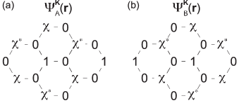
Since we are interested in the behavior close to the Fermi level, we focus on the bandstructure near the two Dirac points. This will be done in two ways: first a simple calculation is applied to show that the spectrum can be derived from symmetry arguments alone. This is confirmed using a tight-binding calculation, which is also easier to generalize to the case with broken symmetry, as in a nanotube.
B.1.1 The derivation
The calculation for graphene DiVincenzo and Mele (1984); Marder (2000) uses the fact that the potential has a unit cell of two carbon atoms and is invariant under translations by lattice vectors as well as under rotation by angle about a lattice symmetry point ( symmetry). At the Dirac points and , we define Bloch states, denoted and , which are eigenstates of the translation operator:
| (46) |
and likewise for . They are degenerate because of the inversion symmetry (which interchanges and and and ). The relative phase between two sites separated by the unit vector is given by
| (47) |
and by for . Symmetry allows the functions to be chosen as eigenstates of the rotations around a center of a hexagon in the following way:
| (48) |
(At the point, one should replace by .)
We now derive an effective Hamiltonian using perturbation theory. Expanding the Bloch Hamiltonian around the Dirac points, we write and
| (49) |
where for the point. At the functions and are degenerate and we define our energy scale so that . The correction to the Hamiltonian is
| (50) |
with being the momentum operator. In the basis, one can now find the matrix elements of the momentum operator , where both take the values or . Each matrix element is a vector in the - plane of the graphene sheet. The component follows from the rotational symmetry of the wave functions:
| (51) |
The eigenvectors in Eq. (51) are
| (52) |
The diagonal elements and vanish, since they obey an analogous equation to Eq. (51), but with replaced by 1, which only has zero solutions.
The low-energy Hamiltonian (50) is thus
| (53) |
where the Fermi velocity was introduced as a phenomenological parameter, to match Eq. (1). Here are the usual Pauli matrices, now working in the sublattice. To describe the Hilbert space spanned by the valley index and sublattice spinor some authors use the terms isospin and pseudospin. However, there is no established convention as to which is which; see opposite definitions for example in Kane and Mele (1997); McCann et al. (2006).
B.1.2 The tight binding derivation
In the tight binding approach the starting point is the Bloch functions of and sublattices:
| (54) |
where are the local basis functions444444These functions are not orthogonal. The overlap matrix should therefore in principle be included when solving Schrödinger’s equation (57). However, it turns out to be higher order in and we can neglect it here. for atomic orbitals at sites and , respectively (see Fig. 55). Neighbouring orbitals hybridize via bonds along direction with overlap matrix elements , with . The Hamiltonian overlap of and is therefore
| (55) |
For graphene, rotational symmetry means all bonds are wquivalent (), and expanding around the point gives (using the definitions in Table I):
| (56) |
To be consistent with the result (53), we then make a transformation of the phase of the basis states so that , which recovers the Hamiltonian (53).
B.1.3 Graphene wave functions
Solving for the eigenenergies and eigenstates of the low-energy Hamiltonian (53)
| (57) |
one finds that the energies are , with the upper (lower) sign corresponding to the conduction (valence) band. The corresponding eigenstates are “spinors” in space:
| (58) |
The spinor gives the weights of the sublattice Bloch states (54). The wave function near is thus
| (59) |
which can be separated into a fast and a slow part:
| (60) |
where the plane wave part is the so-called envelope function. Of course, a similar relation holds near .
B.2 Nanotubes: Graphene on a cylinder
One must take care when transforming from the graphene coordinates to the nanotube cylindrical coordinates. Above we used the coordinate system defined in Table I, i.e. the horizontal bonds in Fig. 55 are along our -direction. When changing to the coordinate system , the coordinates are rotated as:
| (61) |
where is the angle between and , or in terms of the chiral angle . In these coordinates, Eq. (53) becomes
| (62) |
The coordinate rotation thus creates a phase factor , which can be removed by a unitary transformation. Doing this, we get the nanotube Hamiltonian in cylindrical coordinates:
| (63) |
where the unitary operator is
| (64) |
The Hamiltonian (63) has eigenenergies .
When graphene is rolled up to a nanotube (Fig. 1), the wave functions are restricted by periodic boundary conditions (), implying that
| (65) |
The condition for a metallic nanotube is that the spectrum of the Hamiltonian (63) is gapless, i.e. . This happens when , where is an integer. From the definitions in Table I, this is equivalent to (Fig. 5).
B.3 The curvature-induced gap
Deformation of graphene due to nanotube curvature causes the overlap matrix elements to depend on direction, breaking the rotational symmetry. Because the effect on the Dirac cones is to shift them in momentum space Kane and Mele (1997), graphene remains ungapped when curved. However, in a nominally metallic nanotube, this shift opens a band gap (Fig. 8). To understand these effects, we return to the degenerate subspace and calculate the correction to first order in the curvature perturbation . First, we see the diagonal matrix elements are equal454545This is because the combination of inversion and time-reversal symmetries rules out a term in the Hamiltonian., . Next, using the tight-binding wave functions, we find the off-diagonal elements are
| (66) |
where is the curvature correction to the hopping matrix elements for the three bonds. Since is zero for a bond parallel to the nanotube axis and maximal for one perpendicular to it, the leading angular dependence is , where is the angle between the bond and the chiral vector. Equation (66) then evaluates to
| (67) |
with replaced by in the valley. Applying the same transformation that led from Eq. (56) to Eq. (53) and changing the phase as explained below Eq. (56), we obtain the curvature correction in cylindrical coordinates:
| (70) | |||||
| (71) |
When this is added to the Hamiltonian (63), it is clear that both and are shifted. However, the shift in is unimportant and can be absorbed into the longitudinal momentum, whereas the shift in (the coefficient to ) gives a gap in the nanotube spectrum as shown in Fig. 8.
B.4 Spin-orbit coupling
We now include the effect of spin-orbit coupling. Special relativity tells us that an electric field is experienced by a moving electron as a magnetic field. The resulting spin-orbit interaction (SOI) Hamiltonian is given by
| (72) |
where is the electric field and is a constant derived from relativistic quantum mechanics. Each carbon ion contributes to , giving rise to matrix elements between -orbitals and in-plane orbitals, which in turn are coupled by curvature. To describe this based on microscopic parameters, one must start from the known atomic spin-orbit coupling of carbon and the tight-binding parameters. However, since we do not aim to determine the size of the effect, we use a simpler approach, namely to introduce phenomenological parameters for the SOI-induced coupling between orbitals in curved graphene. In this approach, the perturbation (72) gives matrix elements in the Bloch basis (59).
As explained in Sec. III.F.1, broken symmetry in the nanotube allows the first-order matrix elements to be non-zero. Consider the simplest way to break mirror symmetry, namely a constant radial electric field . We need to calculate the matrix elements of the spin-orbit Hamiltonian (72) in the basis. Taking the cross product in Eq. (72) and projecting to the parallel direction gives
| (73) |
where we used the matrix element of from Eq. (52) and the rotation (61). This also holds for the valley, if is replaced by . After the unitary transformation (64), we obtain the form of the orbital-like spin-orbit interaction in cylindrical coordinates:
| (74) |
where is a phenomenological parameter. As we said, this derivation is based only on symmetry and gives no information about the magnitude of , except that it is linear in the atomic SOI and inversely proportional to nanotube diameter. Thus the orbital-like SOI has an easy physical interpretation: it is caused by a Rashba effect, because it is proportional to the azimuthal momentum and the (mean) radial electric field. This is the SOI that was originally derived for graphene Kane and Mele (1997) and for nanotubes Ando (2000).
It was realized later that one more term is allowed by the reduced symmetry (see III.6.3). This term comes from the diagonal matrix elements:
| (75) |
and the identical expression for the sublattice. For a constant electric field (or one obeying the symmetry) is zero. When the rotational symmetry is broken, it can be non-zero. It turns out that depends on the chirality. We study two special cases: armchair and zig-zag nanotubes.
Armchair nanotubes have mirror planes perpendicular to the nanotube axis through an atom. Therefore the curvature-induced electric field has the same symmetry, and so does . Using that the wave function transforms under reflection as , as evident from Fig. 55, we have for armchair nanotubes:
| (76) |
and therefore purely imaginary. On the other hand, since the operator is Hermitian, we must also have . Hence for an armchair nanotube .
Zig-zag nanotubes have no mirror plane through an atom and perpendicular to the axis. Instead, there is a mirror plane along the axis, and since changes sign under this symmetry, there is no cancellation as for the armchair case.
We conclude that there is a spin-orbit-interaction contribution diagonal in pseudospin, of the form
| (77) |
where depends on chirality and therefore has leading harmonic . This is the Zeeman-like term of Eq. (18), which thus comes from intra-sublattice matrix elements, i.e. from next-nearest neighbor couplings.
B.5 Final form of the Hamiltonian
The final low-energy Hamiltonian is the sum of the metallic nanotube Hamiltonian, the curvature term, and the two spin-orbit terms:
| (78) |
where both and are proportional to . In addition, a magnetic field gives rise to an Aharonov-Bohm phase, as well as the usual Zeeman term:
| (79) |
with . The spectrum can be found by simple diagonalization of the Hamiltonian, giving the expression in Eq. (20) for for the case of directed along the nanotube. In that equation the gap is and the confinement energy is . The convention used here has for the time reversal operator , where denotes complex conjugation. Time reversal therefore transforms , , , and .464646Some authors use a convention where , . This is equivalent to a unitary transformation , with . This also changes the definition of the time-reversal operator to , such that time reversal corresponds to a sign change of and .
B.6 Single-particle quantum dot states
Next we discuss the single-particle states in a quantum dot. We assume a parallel magnetic field (making the spin projection along the axis a good quantum number) and a potential that is flat in the middle of the dot. The wave function is thus a superposition of right-moving and left-moving waves. In principle, both plane wave solutions close to and should be included, because the dot terminations can mix the two valleys. However, we approximate the valley index a good quantum number, assuming a smooth confining potential, and later include mixing via a matrix element between the valley-polarized states, as explained in Sec. III.B. The standing wave is then of the form
| (80) |
where is the periodic part of the Bloch wave function, and where the relation between and is determined by the reflection coefficients and at the ends of the dot, because the condition for a bound state is . Importantly, the envelope wave function depends on valley and spin, because depends on both through the energy:
| (81) |
(Here .) For , we thus have two Kramers doublets separated by an energy , as explained in the main text. We emphasize that because of the spin-orbit induced difference in , the two doublets cannot be exactly written as product states of longitudinal, valley, and spin components.
In the main text, we refer to the single-particle states as , where is a quantum number that labels the solutions to the above problem. Two-electron states are then built from the two-electron Slater determinants: as in Table 4. These states do not take into account that the longitudinal wave functions are easily distorted by Coulomb interactions, resulting in highly correlated two-electron states (cf. Sec. VII).
B.7 Two-electron states and exchange interaction
In a two-electron quantum dot the question of interaction corrections to the simple single-particle filling arises. We will discuss these corrections using first-order perturbation theory. The two-electron matrix element between four states and has the form:
| (82) |
where
| (83) |
and is the Coulomb interaction potential. The state is a simple product state: and not an antisymmetrized state as in the headers of Table IV. This matrix element between two Bloch states in Eq. (59) is
| (84) |
where is a normalization equal to the number of unit cells and where we have neglected contributions from the overlap of neighboring atoms. The Coulomb matrix element obtained by inserting Eq. (83) into (82) naturally separates into a short and a long-range part . The two contributions are
| (85a) | |||||
| (85b) | |||||
where and where is a normalization area of the nanotube surface. For a quantum dot of length and diameter , the short-range part is , which for parameters nm, nm, and eV gives meV.
B.8 Exchange integrals due to long-range Coulomb interaction
Rotational symmetry can be used to show that the long-range part vanishes except when , which in terms of valley index means Weiss et al. (2010). This valley selection rule contrasts with that for spin, which is and . Separating both the wave vectors and the coordinates into a transverse part and a longitudinal part, it becomes evident that the rapid oscillations of the Bloch wave functions make it a good approximation to ignore terms off-diagonal in valley indices, because
| (86) |
where the condition was used and where is an integer. Therefore, it is generally true that for narrow-gap nanotubes, which have , the Coulomb matrix element is strongly suppressed.
Turning to the case of two electrons in a single dot, occupying single-particle states in symmetric or antisymmetric combinations as discussed in Sec. IV, the matrix elements between such orbitals therefore obey
| (87) |
This equation can be applied to calculate the long-range interaction energies of the states in Table IV. For the states, we get four terms. The cross terms vanish, because they cannot have and at the same time. We therefore conclude that there are only diagonal, direct Coulomb interaction terms, i.e. no exchange corrections. Assuming the charge distribution of both Kramers pairs to be approximately the same, we thus have
| (88) |
Consider now the symmetric states containing different longitudinal modes, . There are now eight terms in the interaction integral. The non-zero terms have the same valley and spin for the same electron label. If and , there are two positive cross terms. The same is true if and (because of the fast oscillations that lead to Eq. (87)). We therefore conclude:
| (89) |
where
| (90) |
is an exchange-like Coulomb integral.
The situation is similar for the antisymmetric states , except now the sign is opposite, i.e. there is an energy reduction due to exchange integrals. These energy shifts can be absorbed into the definition of and , which is what is done in Table IV.
B.9 Exchange integrals due to short-range Coulomb interaction
For the short-range Coulomb interaction the valley selection rules in Eq. (87) do not apply. Within the multiplet we find that states with antiparallel spin are raised in energy, assuming a repulsive short-range interaction . This is because in such a state, two electrons can occupy the same atomic site, in contrast to the spin-polarized states where spatial antisymmetry forbids this.
The antisymmetric states are almost unaltered by the short range interaction Secchi and Rontani (2013), because their longitudinal symmetries differ from those in . This can be intuitively understood by considering the limit , which allows us to separate each two-electron wave function into a longitudinal part and a spin-valley part. In this limit, states have zero amplitude to occupy the same cross section of nanotube and therefore the same atomic site. As an example, consider the valley-polarized state . For it can be rewritten as , with asymmetric longitudinal part as expected. In contrast, the analogous state in is longitudinally symmetric: .
B.10 Two-electron states and Pauli blockade
In Sec. IV we discussed Pauli blockade of two-electron states at zero magnetic field. We noted that for some of the blocked states Pauli blockade can be lifted by a dephasing mechanism only, whereas other blocked states require that the spin or valley quantum number within one of the dots be flipped. Here we give some examples.
As an example for dephasing, consider the blocked state . From Table 4 we can write out the wave function by identifying (2) with the lowest longitudinal shell in the right(left) dot. After rearranging some terms this state has the form:
| (91) |
We are interested in the time evolution of this state, and model dephasing by assuming an effective Kramers splitting in the left dot that is slightly larger than that in the right dot: . Up to a trivial dynamical phase, the state evolves with time to:
| (92) |
When the blocked state has dephased into the unblocked state . This is similar to the rapid dephasing from to due to an Overhauser field difference in a conventional double dot.
Next, consider the blocked state . We show that a valley flip in either dot will lift Pauli blockade. We can write out the state as
| (93) |
A valley flip in e.g. the left dot () leads to the state
| (94) |
which is a superposition of and the unblocked state . Alternatively, a spin flip in the left dot results in a superposition of and , whereas a combined spin-valley flip results in a superposition of and . In all cases, Pauli blockade is circumvented by the admixture of unblocked states (i.e. longitudinal symmetric states). However, because of spin-orbit coupling, a single flip in one of the dots requires emission or absorption of energy, whereas a spin-and-valley flip may be allowed by energy conservation. Therefore, “spin-valley” blockade can occur not primarily due to spin and valley conservation, but due to energy conservation. Thus energy conservation plays a central role in establishing Pauli blockade, just as in conventional quantum dots (cf. Fig. 27). In nanotubes the relevant energy scale is the spin-orbit energy rather than the orbital level spacing. Therefore, Pauli blockade in nanotubes is generically weaker than singlet-triplet Pauli blockade in conventional semiconductors.
References
- Ajiki and Ando (1993) Ajiki, H., and T. Ando (1993), J. Phys. Soc. Jpn. 62, 1255.
- Allen et al. (2011) Allen, C. S., M. D. Elkin, G. Burnell, B. J. Hickey, C. Zhang, S. Hofmann, and J. Robertson (2011), Phys. Rev. B 84, 115444.
- Amer et al. (2013) Amer, M. R., S.-W. Chang, R. Dhall, J. Qiu, and S. B. Cronin (2013), Nano Lett. 13, 5129.
- Anders et al. (2008) Anders, F., D. Logan, M. Galpin, and G. Finkelstein (2008), Phys. Rev. Lett. 100, 086809.
- Ando (2000) Ando, T. (2000), J. Phys. Soc. Jpn. 69, 1757.
- Ando and Nakanishi (1998) Ando, T., and T. Nakanishi (1998), J. Phys. Soc. Jpn. 67, 1704.
- Ando et al. (1998) Ando, T., T. Nakanishi, and R. Saito (1998), J. Phys. Soc. Jpn. 67, 2857.
- Auslaender et al. (2005) Auslaender, O. M., H. Steinberg, A. Yacoby, Y. Tserkovnyak, B. I. Halperin, K. W. Baldwin, L. N. Pfeiffer, and K. W. West (2005), Science 308, 88.
- Averin and Nazarov (1992) Averin, D., and Y. Nazarov (1992), in Single Charge Tunneling: Coulomb Blockade Phenomena in Nanostructures, edited by H. Grabert and M. H. Devoret (Plenum Press and NATO Scientific Affairs Division, New York) pp. 217–247.
- Balakrishnan et al. (2013) Balakrishnan, J., G. K. Koon, M. Jaiswal, A. H. Neto, and B. Özyilmaz (2013), Nat. Phys. 9, 284.
- Balder (2008) Balder, T. (2008), Modelling Quantum Dots in Realistic Carbon Nanotube Devices, Master’s thesis (Delft University of Technology).
- Baskin and Meyer (1955) Baskin, Y., and L. Meyer (1955), Phys. Rev. 100, 544.
- Benyamini et al. (2014) Benyamini, A., A. Hamo, S. V. Kusminskiy, F. von Oppen, and S. Ilani (2014), Nat. Phys. 10, 151.
- Bercioux et al. (2011) Bercioux, D., G. Buchs, H. Grabert, and O. Gröning (2011), Phys. Rev. B 83, 165439.
- van den Berg et al. (2013) van den Berg, J. W. G., S. Nadj-Perge, V. S. Pribiag, S. R. Plissard, E. Bakkers, S. M. Frolov, and L. P. Kouwenhoven (2013), Phys. Rev. Lett. 110, 066806.
- Bezryadin et al. (1998) Bezryadin, A., A. Verschueren, S. J. Tans, and C. Dekker (1998), Phys. Rev. Lett. 80, 4036.
- Biercuk et al. (2005) Biercuk, M., S. Garaj, N. Mason, J. Chow, and C. Marcus (2005), Nano Lett. 5, 1267.
- Biercuk et al. (2008) Biercuk, M., S. Ilani, C. Marcus, and P. L. McEuen (2008), in Carbon Nanotubes, Topics in Applied Physics (Springer-Verlag, Berlin Heidelberg) pp. 455–493.
- Biercuk et al. (2004) Biercuk, M., N. Mason, J. Chow, and C. Marcus (2004), Nano Lett. 4, 2499.
- Biercuk et al. (2006) Biercuk, M., D. Reilly, T. Buehler, V. Chan, J. Chow, R. Clark, and C. Marcus (2006), Phys. Rev. B 73, 201402.
- Blase et al. (1994) Blase, X., L. X. Benedict, E. L. Shirley, and S. G. Louie (1994), Phys. Rev. Lett. 72, 1878.
- Bluhm et al. (2011) Bluhm, H., S. Foletti, I. Neder, M. S. Rudner, D. Mahalu, V. Umansky, and A. Yacoby (2011), Nat. Phys. 7, 109.
- Bockrath et al. (1997) Bockrath, M., D. Cobden, P. McEuen, N. Chopra, A. Zettl, A. Thess, and R. E. Smalley (1997), Science 275, 1922.
- Bockrath et al. (1999) Bockrath, M., D. H. Cobden, J. Lu, A. G. Rinzler, R. E. Smalley, L. Balents, and P. L. McEuen (1999), Nature (London) 397, 598.
- Bolotin et al. (2008) Bolotin, K. I., K. J. Sikes, Z. Jiang, M. Klima, G. Fudenberg, J. Hone, P. Kim, and H. L. Stormer (2008), Solid State Commun. 146, 351.
- Bomze et al. (2010) Bomze, Y., I. Borzenets, H. Mebrahtu, A. Makarovski, H. U. Baranger, and G. Finkelstein (2010), Phys. Rev. B 82, 161411.
- Borda et al. (2003) Borda, L., G. Zaránd, W. Hofstetter, B. I. Halperin, and J. von Delft (2003), Phys. Rev. Lett. 90, 026602.
- Borysenko et al. (2008) Borysenko, K. M., Y. G. Semenov, and K. W. Kim (2008), Phys. Rev. B 77, 205402.
- Bozovic et al. (2001) Bozovic, D., M. Bockrath, J. H. Hafner, C. M. Lieber, H. Park, and M. Tinkham (2001), Appl. Phys. Lett. 78, 3693.
- Braunecker et al. (2013) Braunecker, B., P. Burset, and A. Levy Yeyati (2013), Phys. Rev. Lett. 111, 136806.
- Buitelaar et al. (2002a) Buitelaar, M. R., A. Bachtold, T. Nussbaumer, M. Iqbal, and C. Schönenberger (2002a), Phys. Rev. Lett. 88, 156801.
- Buitelaar et al. (2002b) Buitelaar, M. R., T. Nussbaumer, and C. Schönenberger (2002b), Phys. Rev. Lett. 89, 256801.
- Bulaev et al. (2008) Bulaev, D., B. Trauzettel, and D. Loss (2008), Phys. Rev. B 77, 235301.
- Büsser and Martins (2007) Büsser, C., and G. Martins (2007), Phys. Rev. B 75, 045406.
- Büsser et al. (2011) Büsser, C. A., E. Vernek, P. Orellana, G. A. Lara, E. H. Kim, A. E. Feiguin, E. V. Anda, and G. B. Martins (2011), Phys. Rev. B 83, 125404.
- Cao et al. (2005) Cao, J., Q. Wang, and H. J. Dai (2005), Nat. Mater. 4, 745.
- Cao et al. (2004) Cao, J., Q. Wang, M. Rolandi, and H. J. Dai (2004), Phys. Rev. Lett. 93, 216803.
- Castro Neto et al. (2009) Castro Neto, A., F. Guinea, N. Peres, and K. S. Novoselov (2009), Rev. Mod. Phys. 81, 109.
- Babić et al. (2004) Babić, B., T. Kontos, and C. Schönenberger (2004), Phys. Rev. B 70, 235419.
- Chang and Chen (2009) Chang, A. M., and J. C. Chen (2009), Rep. Prog. Phys. 72, 096501.
- Charlier et al. (2007) Charlier, J. C., X. Blase, and S. Roche (2007), Rev. Mod. Phys. 79, 677.
- Chico et al. (2009) Chico, L., M. P. López-Sancho, and M. C. Munoz (2009), Phys. Rev. B 79, 235423.
- Choi et al. (2005) Choi, M.-S., R. López, and R. Aguado (2005), Phys. Rev. Lett. 95, 067204.
- Chorley et al. (2012) Chorley, S. J., M. R. Galpin, F. W. Jayatilaka, C. G. Smith, D. E. Logan, and M. R. Buitelaar (2012), Phys. Rev. Lett. 109, 156804.
- Churchill (2012) Churchill, H. O. H. (2012), PhD Thesis (Harvard University) .
- Churchill et al. (2009a) Churchill, H. O. H., A. J. Bestwick, J. W. Harlow, F. Kuemmeth, D. Marcos, C. H. Stwertka, S. K. Watson, and C. M. Marcus (2009a), Nat. Phys. 5, 321.
- Churchill et al. (2009b) Churchill, H. O. H., F. Kuemmeth, J. W. Harlow, A. J. Bestwick, E. I. Rashba, K. Flensberg, C. H. Stwertka, T. Taychatanapat, S. K. Watson, and C. M. Marcus (2009b), Phys. Rev. Lett. 102, 166802.
- Cleuziou et al. (2013) Cleuziou, J. P., N. G. N’Guyen, S. Florens, and W. Wernsdorfer (2013), Phys. Rev. Lett. 111, 136803.
- Coish and Qassemi (2011) Coish, W. A., and F. Qassemi (2011), Phys. Rev. B 84, 245407.
- Cottet et al. (2006) Cottet, A., T. Kontos, S. Sahoo, H. T. Man, M.-S. Choi, W. Belzig, C. Bruder, A. F. Morpurgo, and C. Schönenberger (2006), Semicond. Sci. Technol. 21, S78.
- Cronenwett et al. (1998) Cronenwett, S. M., T. H. Oosterkamp, and L. P. Kouwenhoven (1998), Science 281, 540.
- Cywiński et al. (2012) Cywiński, L., R. Lutchyn, C. Nave, and S. Das Sarma (2012), Nature 488, 61.
- Danon and Nazarov (2009) Danon, J., and Y. Nazarov (2009), Phys. Rev. B 80, 041301.
- Delbecq et al. (2011) Delbecq, M. R., V. Schmitt, F. D. Parmentier, N. Roch, J. J. Viennot, G. Feve, B. Huard, C. Mora, A. Cottet, and T. Kontos (2011), Phys. Rev. Lett. 107, 256804.
- Deshpande and Bockrath (2008) Deshpande, V. V., and M. Bockrath (2008), Nat. Phys. 4, 314.
- Deshpande et al. (2010) Deshpande, V. V., M. Bockrath, L. Glazman, and A. Yacoby (2010), Nature 464, 209.
- Deshpande et al. (2009) Deshpande, V. V., B. Chandra, R. Caldwell, D. S. Novikov, J. Hone, and M. Bockrath (2009), Science 323, 106.
- Dial et al. (2013) Dial, O. E., M. D. Shulman, S. P. Harvey, and H. Bluhm (2013), Phys Rev Lett 110, 146804.
- DiVincenzo and Mele (1984) DiVincenzo, D. P., and E. Mele (1984), Phys. Rev. B 29, 1685.
- Dora et al. (2008) Dora, B., M. Gulacsi, J. Koltai, V. Zolyomi, J. Kurti, and F. Simon (2008), Phys. Rev. Lett. 101, 106408.
- Du et al. (2008) Du, X., I. Skachko, A. Barker, and E. Y. Andrei (2008), Nat. Nanotechnol. 3, 491.
- Elias et al. (2009) Elias, D. C., R. R. Nair, T. M. G. Mohiuddin, S. Morozov, P. Blake, M. P. Halsall, A. C. Ferrari, D. W. Boukhvalov, M. I. Katsnelson, A. K. Geim, and K. S. Novoselov (2009), Science 323, 610.
- Eto and Nazarov (2000) Eto, M., and Y. V. Nazarov (2000), Phys. Rev. Lett. 85, 1306.
- Fang et al. (2008) Fang, T.-F., W. Zuo, and H.-G. Luo (2008), Phys. Rev. Lett. 101, 246805.
- Fang et al. (2010) Fang, T.-F., W. Zuo, and H.-G. Luo (2010), Phys. Rev. Lett. 104, 169902.
- Fischer et al. (2009) Fischer, J., B. Trauzettel, and D. Loss (2009), Phys. Rev. B 80, 155401.
- Flensberg (2006) Flensberg, K. (2006), New J. Phys. 8, 5.
- Flensberg and Marcus (2010) Flensberg, K., and C. M. Marcus (2010), Phys. Rev. B 81, 195418.
- de Franceschi et al. (2010) de Franceschi, S., L. P. Kouwenhoven, C. Schönenberger, and W. Wernsdorfer (2010), Nat. Nanotechnol. 5, 703.
- Galland and Imamoğlu (2008) Galland, C., and A. Imamoğlu (2008), Phys. Rev. Lett. 101, 157404.
- Galpin et al. (2010) Galpin, M., F. Jayatilaka, D. Logan, and F. Anders (2010), Phys. Rev. B 81, 075437.
- Goldhaber-Gordon et al. (1998a) Goldhaber-Gordon, D., J. Göres, M. A. Kastner, H. Shtrikman, D. Mahalu, and U. Meirav (1998a), Phys. Rev. Lett. 81, 5225.
- Goldhaber-Gordon et al. (1998b) Goldhaber-Gordon, D., H. Shtrikman, D. Mahalu, D. Abusch-Magder, U. Meirav, and M. A. Kastner (1998b), Nature (London) 391, 156.
- Gotz et al. (2008) Gotz, G., G. A. Steele, W.-J. Vos, and L. P. Kouwenhoven (2008), Nano Lett. 8, 4039.
- Gräber et al. (2006) Gräber, M. R., W. A. Coish, C. Hoffmann, M. Weiss, J. Furer, S. Oberholzer, D. Loss, and C. Schönenberger (2006), Phys. Rev. B 74, 075427.
- Greilich et al. (2006) Greilich, A. R., D. R. Yakovlev, A. Shabaev, A. L. Efros, I. A. Yugova, R. Oulton, V. Stavarache, D. Reuter, A. Wieck, and M. Bayer (2006), Science 313, 341.
- Grobis et al. (2007) Grobis, M., I. G. Rau, R. M. Potok, and D. Goldhaber-Gordon (2007), in Handbook of Magnetism and Advanced Magnetic Materials (Wiley).
- Grove-Rasmussen et al. (2012) Grove-Rasmussen, K., S. Grap, J. Paaske, K. Flensberg, S. Andergassen, V. Meden, H. Jørgensen, K. Muraki, and T. Fujisawa (2012), Phys. Rev. Lett. 108, 176802.
- Grove-Rasmussen et al. (2007) Grove-Rasmussen, K., H. Jørgensen, and P. Lindelof (2007), Physica E 40, 92.
- Hamada et al. (1992) Hamada, N., S. Sawada, and A. Oshiyama (1992), Phys. Rev. Lett. 68, 1579.
- Hanson et al. (2007) Hanson, R., L. P. Kouwenhoven, J. R. Petta, S. Tarucha, and L. M. K. Vandersypen (2007), Rev. Mod. Phys. 79, 1217.
- Hauptmann et al. (2008) Hauptmann, J. R., J. Paaske, and P. E. Lindelof (2008), Nat. Phys. 4, 373.
- Heikkila (2013) Heikkila, T. T. (2013), The Physics of Nanoelectronics: Transport and Fluctuation Phenomena at Low Temperatures (Oxford University Press).
- Heinze et al. (2002) Heinze, S., J. Tersoff, R. Martel, V. Derycke, J. Appenzeller, and P. Avouris (2002), Phys. Rev. Lett. 89, 106801.
- Heyd et al. (1997) Heyd, R., A. Charlier, and E. McRae (1997), Phys. Rev. B 55, 6820.
- Hofstadter (1976) Hofstadter, D. R. (1976), Phys. Rev. B 14, 2239.
- Holleitner et al. (2004) Holleitner, A. W., A. Chudnovskiy, D. Pfannkuche, K. Eberl, and R. H. Blick (2004), Phys. Rev. B 70, 075204.
- Holm et al. (2008) Holm, J. V., H. I. Jørgensen, K. Grove-Rasmussen, J. Paaske, K. Flensberg, and P. E. Lindelof (2008), Phys. Rev. B 77, 161406.
- Huang et al. (2008) Huang, M., Y. Wu, B. Chandra, H. Yan, Y. Shan, T. F. Heinz, and J. Hone (2008), Phys. Rev. Lett. 100, 136803.
- Huang et al. (2005) Huang, X. M. H., R. Caldwell, L. Huang, S. C. Jun, M. Huang, M. Y. Sfeir, S. P. O’Brien, and J. Hone (2005), Nano Lett. 5, 1515.
- Huertas-Hernando et al. (2006) Huertas-Hernando, D., F. Guinea, and A. Brataas (2006), Phys. Rev. B 74, 155426.
- Huttel et al. (2009) Huttel, A. K., G. A. Steele, B. Witkamp, M. Poot, L. P. Kouwenhoven, and H. S. J. van der Zant (2009), Nano Lett. 9, 2547.
- Ihn (2010) Ihn, T. (2010), Semiconductor Nanostructures: Quantum states and electronic transport (Oxford University Press, Oxford).
- Ilani et al. (2006) Ilani, S., L. A. K. Donev, M. Kindermann, and P. L. Mceuen (2006), Nat. Phys. 2, 687.
- Ilani and McEuen (2010) Ilani, S., and P. McEuen (2010), Ann. Rev. Cond. Matt. Phys. 1, 1.
- Imambekov et al. (2012) Imambekov, A., T. L. Schmidt, and L. I. Glazman (2012), Rev. Mod. Phys. 84, 1253.
- Ingold and Nazarov (1992) Ingold, G.-L., and Y. V. Nazarov (1992), in NATO ASI Series B: Physics, vol. 294, Single Charge Tunneling (Plenum, New York) pp. 21–106.
- Ivchenko and Spivak (2002) Ivchenko, E. L., and B. Spivak (2002), Phys. Rev. B 66, 155404.
- Izumida et al. (2001) Izumida, W., O. Sakai, and S. Tarucha (2001), Phys. Rev. Lett. 87, 216803.
- Izumida et al. (2009) Izumida, W., K. Sato, and R. Saito (2009), J. Phys. Soc. Jpn. 78, 074707.
- Izumida et al. (2012) Izumida, W., A. Vikström, and R. Saito (2012), Phys. Rev. B 85, 165430.
- Jarillo-Herrero et al. (2005a) Jarillo-Herrero, P. D., J. Kong, H. S. J. van der Zant, C. Dekker, L. P. Kouwenhoven, and S. de Franceschi (2005a), Phys. Rev. Lett. 94, 156802.
- Jarillo-Herrero et al. (2005b) Jarillo-Herrero, P. D., J. Kong, H. S. J. van der Zant, C. Dekker, L. P. Kouwenhoven, and S. de Franceschi (2005b), Nature (London) 434, 484.
- Jarillo-Herrero et al. (2004) Jarillo-Herrero, P. D., S. Sapmaz, C. Dekker, L. P. Kouwenhoven, and H. S. J. van der Zant (2004), Nature (London) 429, 389.
- Jauregui et al. (1993) Jauregui, K., W. Häusler, and B. Kramer (1993), Europhys. Lett.) 24, 581.
- Jeong and Lee (2009) Jeong, J.-S., and H.-W. Lee (2009), Phys. Rev. B 80, 075409.
- Jespersen et al. (2011a) Jespersen, T. S., K. Grove-Rasmussen, K. Flensberg, J. Paaske, K. Muraki, T. Fujisawa, and J. Nygård (2011a), Phys. Rev. Lett. 107.
- Jespersen et al. (2011b) Jespersen, T. S., K. Grove-Rasmussen, J. Paaske, K. Muraki, T. Fujisawa, J. Nygård, and K. Flensberg (2011b), Nat. Phys. 7, 348.
- Jhang et al. (2011) Jhang, S. H., M. Marganska, Y. Skourski, D. Preusche, M. Grifoni, J. Wosnitza, and C. Strunk (2011), Phys. Rev. Lett. 106, 096802.
- Jhang et al. (2010) Jhang, S. H., M. Marganska, Y. Skourski, D. Preusche, B. Witkamp, M. Grifoni, H. van der Zant, J. Wosnitza, and C. Strunk (2010), Phys. Rev. B 82, 041404.
- Johnson et al. (2005) Johnson, A., J. R. Petta, J. M. Taylor, A. Yacoby, M. D. Lukin, C. M. Marcus, M. P. Hanson, and A. C. Gossard (2005), Nature 435, 925.
- Jørgensen et al. (2008) Jørgensen, H. I., K. Grove-Rasmussen, K. Y. Wang, A. M. Blackburn, K. Flensberg, P. E. Lindelof, and D. A. Williams (2008), Nat. Phys. 4, 536.
- Jung et al. (2013) Jung, M., J. Schindele, S. Nau, M. Weiss, A. Baumgartner, and C. Schönenberger (2013), Nano Lett. 13, 4522.
- Kane and Mele (2004) Kane, C., and E. Mele (2004), Phys. Rev. Lett. 93, 197402.
- Kane and Mele (1997) Kane, C. L., and E. J. Mele (1997), Phys. Rev. Lett. 78, 1932.
- Kane and Mele (2005) Kane, C. L., and E. J. Mele (2005), Phys. Rev. Lett. 95, 226801.
- Keller et al. (2013) Keller, A. J., S. Amasha, I. Weymann, C. P. Moca, I. G. Rau, J. A. Katine, H. Shtrikman, G. Zaránd, and D. Goldhaber-Gordon (2013), Nat. Phys. 10, 145.
- Khaetskii and Nazarov (2001) Khaetskii, A. V., and Y. V. Nazarov (2001), Phys. Rev. B 64.
- Kim et al. (2003) Kim, W., A. Javey, O. Vermesh, Q. Wang, Y. Li, and H. Dai (2003), Nano Lett. 3, 193.
- Kiršanskas et al. (2012) Kiršanskas, G., J. Paaske, and K. Flensberg (2012), Phys. Rev. B 86, 075452.
- Kleiner and Eggert (2001) Kleiner, A., and S. Eggert (2001), Phys. Rev. B 64, 113402.
- Klinovaja et al. (2011a) Klinovaja, J., M. Schmidt, B. Braunecker, and D. Loss (2011a), Phys. Rev. B 84, 085452.
- Klinovaja et al. (2011b) Klinovaja, J., M. J. Schmidt, B. Braunecker, and D. Loss (2011b), Phys. Rev. Lett. 106, 156809.
- Kociak et al. (2002) Kociak, M., K. Suenaga, K. Hirahara, Y. Saito, T. Nakahira, and S. Iijima (2002), Phys. Rev. Lett. 89, 155501.
- Kombarakkaran and Pietraß (2008) Kombarakkaran, J., and T. Pietraß (2008), Chem. Phys. Lett. 452, 152.
- Kong et al. (1999) Kong, J., C. Zhou, A. Morpurgo, H. T. Soh, C. F. Quate, C. Marcus, and H. J. Dai (1999), Appl. Phys. A 69, 305.
- Koppens et al. (2005) Koppens, F., J. Folk, J. Elzerman, R. Hanson, L. H. W. van Beveren, I. T. Vink, H. P. Tranitz, W. Wegscheider, L. P. Kouwenhoven, and L. M. K. Vandersypen (2005), Science 309, 1346.
- Koppens et al. (2006) Koppens, F. H. L., C. Buizert, K.-J. Tielrooij, I. T. Vink, K. C. Nowack, T. Meunier, L. P. Kouwenhoven, and L. Vandersypen (2006), Nature (London) 442, 766.
- Koppens et al. (2008) Koppens, F. H. L., K. C. Nowack, and L. M. K. Vandersypen (2008), Phys. Rev. Lett. 100, 236802.
- Kouwenhoven and Glazman (2001) Kouwenhoven, L., and L. Glazman (2001), Phys. World 14 (1), 33.
- Kouwenhoven et al. (2001) Kouwenhoven, L. P., D. Austing, and S. Tarucha (2001), Rep. Prog. Phys. 64, 701.
- Kouwenhoven et al. (1997) Kouwenhoven, L. P., C. M. Marcus, P. L. McEuen, S. Tarucha, R. M. Westervelt, and N. S. Wingreen (1997), in Proceedings of the Advanced Study Institute on Mesoscopic Electron Transport (Kluwer) pp. 1–44.
- Kramida et al. (2013) Kramida, A., Y. Ralchenko, J. Reader, and NIST ASD Team (2013), “NIST Atomic Spectra Database (ver. 5.0), Available: http://physics.nist.gov/asd,” .
- Kuemmeth et al. (2010) Kuemmeth, F., H. O. H. Churchill, P. K. Herring, and C. M. Marcus (2010), Materials Today 13, 18.
- Kuemmeth et al. (2008) Kuemmeth, F., S. Ilani, D. C. Ralph, and P. L. McEuen (2008), Nature (London) 452, 448.
- Lai et al. (2011) Lai, N. S., W. H. Lim, C. H. Yang, F. A. Zwanenburg, W. A. Coish, F. Qassemi, A. Morello, and A. S. Dzurak (2011), Sci. Rep. 1, 110.
- Lai et al. (2014) Lai, R. A., H. O. H. Churchill, and C. M. Marcus (2014), Phys. Rev. B 89, 121303(R).
- Laird et al. (2013) Laird, E. A., F. Pei, and L. P. Kouwenhoven (2013), Nat. Nanotechnol. 8, 565.
- de Lange et al. (2010) de Lange, G., Z. H. Wang, D. Riste, V. V. Dobrovitski, and R. Hanson (2010), Science 330, 60.
- Lassagne et al. (2009) Lassagne, B., Y. Tarakanov, J. Kinaret, D. Garcia-Sanchez, and A. Bachtold (2009), Science 325, 1107.
- Leturcq et al. (2009) Leturcq, R., C. Stampfer, K. Inderbitzin, L. Durrer, C. Hierold, E. Mariani, M. G. Schultz, F. von Oppen, and K. Ensslin (2009), Nat. Phys. 5, 327.
- Li and Zhu (2012) Li, J.-J., and K.-D. Zhu (2012), Sci. Rep. 2, 903.
- Li et al. (2014) Li, Y., S. C. Benjamin, G. A. D. Briggs, and E. A. Laird (2014), Physical Review B 90 (19), 195440.
- Liang et al. (2001) Liang, W., M. Bockrath, D. Bozovic, J. H. Hafner, M. Tinkham, and H. Park (2001), Nature 411, 665.
- Liang et al. (2002) Liang, W., M. Bockrath, and H. Park (2002), Phys. Rev. Lett. 88, 126801.
- Liang et al. (2005) Liang, W., M. Bockrath, and H. Park (2005), Ann. Rev. Phys. Chem. 56, 475.
- Lim et al. (2006) Lim, J. S., M.-S. Choi, M. Y. Choi, R. López, and R. Aguado (2006), Phys. Rev. B 74, 205119.
- Lim et al. (2011) Lim, J. S., R. López, and R. Aguado (2011), Phys. Rev. Lett. 107, 196801.
- Liu et al. (2013) Liu, K., X. Hong, Q. Zhou, C. Jin, J. Li, W. Zhou, J. Liu, E. Wang, A. Zettl, and F. Wang (2013), Nat. Nanotechnol. 8, 917.
- Liu and Fan (2001) Liu, L., and S. Fan (2001), J. Am. Chem. Soc. 123, 11502.
- Lu (1995) Lu, J. (1995), Phys. Rev. Lett. 74, 1123.
- Lunde et al. (2005) Lunde, A., K. Flensberg, and A.-P. Jauho (2005), Phys. Rev. B 71, 125408.
- Luttinger (1963) Luttinger, J. (1963), J. Math. Phys. (N.Y.) 4, 1154.
- Luttinger (1951) Luttinger, J. M. (1951), Phys. Rev. 84, 814.
- Makarovski and Finkelstein (2008) Makarovski, A., and G. Finkelstein (2008), Physica B 403, 1555.
- Makarovski et al. (2007) Makarovski, A., J. Liu, and G. Finkelstein (2007), Phys. Rev. Lett. 99, 066801.
- Makarovski et al. (2007) Makarovski, A., A. Zhukov, J. Liu, and G. Finkelstein (2007), Phys. Rev. B 75, 241407.
- Marder (2000) Marder, M. P. (2000), Condensed Matter Physics (John Wiley and Sons).
- Marganska et al. (2014) Marganska, M., P. Chudzinski, and M. Grifoni (2014), eprint:arXiv:1412.7484 .
- Mariani and von Oppen (2009) Mariani, E., and F. von Oppen (2009), Phys. Rev. B 80, 155411.
- Martinek et al. (2005) Martinek, J., M. Sindel, L. Borda, J. Barnaś, R. Bulla, J. König, G. Schön, S. Maekawa, and J. von Delft (2005), Phys. Rev. B 72, 121302.
- Martinek et al. (2003) Martinek, J., Y. Utsumi, H. Imamura, J. Barnaś, S. Maekawa, J. König, and G. Schön (2003), Phys. Rev. Lett. 91, 127203.
- Mason et al. (2004) Mason, N., M. Biercuk, and C. M. Marcus (2004), Science 303, 655.
- Maune et al. (2012) Maune, B. M., M. G. Borselli, B. Huang, T. D. Ladd, P. W. Deelman, K. S. Holabird, A. A. Kiselev, I. Alvarado-Rodriguez, R. S. Ross, A. E. Schmitz, M. Sokolich, C. A. Watson, M. F. Gyure, and A. T. Hunter (2012), Nature (London) 481, 344.
- Mayrhofer and Grifoni (2008) Mayrhofer, L., and M. Grifoni (2008), Eur. Phys. J. B 63, 43.
- Mazza et al. (2013) Mazza, F., B. Braunecker, P. Recher, and A. Levy Yeyati (2013), Phys. Rev. B 88, 195403.
- McCann and Fal’ko (2004) McCann, E., and V. Fal’ko (2004), J. Phys. Condens. Matter 16, 2371.
- McCann et al. (2006) McCann, E., K. Kechedzhi, V. I. Fal’ko, H. Suzuura, T. Ando, and B. L. Altshuler (2006), Physical Review Letters 97 (14), 146805.
- McEuen et al. (1999) McEuen, P., M. Bockrath, D. Cobden, Y. Yoon, and S. Louie (1999), Phys. Rev. Lett. 83, 5098.
- Mebrahtu et al. (2012) Mebrahtu, H., I. Borzenets, D. E. Liu, H. Zheng, Y. Bomze, A. Smirnov, H. Baranger, and G. Finkelstein (2012), Nature 488, 61.
- Merzbacher (1998) Merzbacher, E. (1998), Quantum Mechanics, 3rd ed. (John Wiley and Sons).
- Min et al. (2006) Min, H., J. E. Hill, N. A. Sinitsyn, B. R. Sahu, L. Kleinman, and A. H. MacDonald (2006), Phys. Rev. B 74, 165310.
- Minot et al. (2004) Minot, E. D., Y. Yaish, V. Sazonova, and P. L. McEuen (2004), Nature (London) 428, 536.
- Minot et al. (2003) Minot, E. D., Y. Yaish, V. Sazonova, J. Y. Park, M. Brink, and P. L. McEuen (2003), Phys. Rev. Lett. 90, 156401.
- Mintmire and White (1995) Mintmire, J., and C. White (1995), Carbon 33, 893.
- Mintmire et al. (1992) Mintmire, J. W., B. I. Dunlap, and C. T. White (1992), Phys. Rev. Lett. 68, 631.
- Mizuno et al. (2009) Mizuno, M., E. H. Kim, and G. B. Martins (2009), Journal of Physics Condensed Matter 21, 292203.
- Na et al. (2005) Na, P., H. Kim, H. So, K. Kong, H. Chang, B. H. Ryu, C. Y, J. O. Lee, B. K. Kim, J. J. Kim, and J. Kim (2005), Appl. Phys. Lett. 87, 093101.
- Nadj-Perge et al. (2010a) Nadj-Perge, S., S. M. Frolov, E. P. A. M. Bakkers, and L. P. Kouwenhoven (2010a), Nature (London) 468, 1084.
- Nadj-Perge et al. (2010b) Nadj-Perge, S., S. M. Frolov, J. W. W. v. Tilburg, J. Danon, Y. V. Nazarov, R. Algra, E. P. A. M. Bakkers, and L. P. Kouwenhoven (2010b), Phys. Rev. B 81, 201305.
- Nazarov and Blanter (2009) Nazarov, Y., and Y. M. Blanter (2009), Quantum Transport: Introduction to Nanoscience (Cambridge University Press).
- Nielsen and Chuang (2000) Nielsen, M., and I. Chuang (2000), Quantum Computation and Quantum Information (Cambridge University Press).
- Nisoli et al. (2007) Nisoli, C., P. E. Lammert, E. Mockensturm, and V. H. Crespi (2007), Phys. Rev. Lett. 99, 045501.
- Nowak et al. (2012) Nowak, M. P., B. Szafran, and F. M. Peeters (2012), Phys. Rev. B 86, 125428.
- Nygård and Cobden (2001) Nygård, J., and D. H. Cobden (2001), eprint arXiv:cond-mat/0105289 .
- Nygård et al. (1999) Nygård, J., D. Cobden, M. Bockrath, P. McEuen, and P. Lindelof (1999), Appl. Phys. A 69, 297.
- Nygård et al. (2000) Nygård, J., D. Cobden, and P. Lindelof (2000), Nature (London) 408, 342.
- Odom et al. (1998) Odom, T. W., J.-L. Huang, P. Kim, and C. M. Lieber (1998), Nature (London) 391, 62.
- Ohm et al. (2012) Ohm, C., C. Stampfer, J. Splettstoesser, and M. R. Wegewijs (2012), Appl. Phys. Lett. 100, 143103.
- Okazaki et al. (2011) Okazaki, Y., S. Sasaki, and K. Muraki (2011), Phys. Rev. B 84, 161305.
- Ono et al. (2002) Ono, K., D. Austing, Y. Tokura, and S. Tarucha (2002), Science 297, 1313.
- Ouyang et al. (2001) Ouyang, M., J.-L. Huang, C. L. Cheung, and C. M. Lieber (2001), Science 292, 702.
- Paaske et al. (2006) Paaske, J., A. Rosch, P. Wölfle, N. Mason, C. M. Marcus, and J. Nygård (2006), Nat. Phys. 2, 460.
- Painter and Ellis (1970) Painter, G., and D. E. Ellis (1970), Phys. Rev. B 1, 4747.
- Pályi and Burkard (2009) Pályi, A., and G. Burkard (2009), Phys. Rev. B 80, 201404.
- Pályi and Burkard (2010) Pályi, A., and G. Burkard (2010), Phys. Rev. B 82, 155424.
- Pályi and Burkard (2011) Pályi, A., and G. Burkard (2011), Phys. Rev. Lett. 106, 086801.
- Pályi et al. (2012) Pályi, A., P. R. Struck, M. Rudner, K. Flensberg, and G. Burkard (2012), Phys. Rev. Lett. 108, 206811.
- Park et al. (1999) Park, C., Y. Kim, and K. Chang (1999), Phys. Rev. B 60, 10656.
- Park et al. (2002) Park, J.-Y., Y. Yaish, M. Brink, S. Rosenblatt, and P. L. McEuen (2002), Appl. Phys. Lett. 80, 4446.
- Pasupathy et al. (2004) Pasupathy, A. N., R. C. Bialczak, J. Martinek, J. E. Grose, L. a. K. Donev, P. L. McEuen, and D. C. Ralph (2004), Science 306, 86.
- Pecker et al. (2013) Pecker, S., F. Kuemmeth, A. Secchi, M. Rontani, D. C. Ralph, P. L. McEuen, and S. Ilani (2013), Nat. Phys. 9, 576.
- Pei et al. (2012) Pei, F., E. A. Laird, G. A. Steele, and L. P. Kouwenhoven (2012), Nat. Nanotechnol. 7, 630.
- Peng et al. (2007) Peng, X., N. Komatsu, S. Bhattacharya, T. Shimawaki, S. Aonuma, T. Kimura, and A. Osuka (2007), Nat. Nanotechnol. 2, 361.
- Pennington and Stenger (1996) Pennington, C. H., and V. A. Stenger (1996), Rev. Mod. Phys. 68, 855.
- Petit et al. (1997) Petit, P., E. Jouguelet, J. Fischer, A. Rinzler, and R. Smalley (1997), Phys. Rev. B 56, 9275.
- Petta et al. (2005) Petta, J. R., A. C. Johnson, J. . Taylor, E. A. Laird, A. Yacoby, M. D. Lukin, C. M. Marcus, M. P. Hanson, and A. C. Gossard (2005), Science 309, 2180.
- Pfund et al. (2007) Pfund, A., I. Shorubalko, K. Ensslin, and R. Leturcq (2007), Phys. Rev. Lett. 99, 036801.
- Pla et al. (2012) Pla, J. J., K. Y. Tan, J. P. Dehollain, W. H. Lim, J. J. L. Morton, D. N. Jamieson, A. S. Dzurak, and A. Morello (2012), Nature (London) 489, 541.
- Postma et al. (2001) Postma, H. W. C., T. Teepen, Z. Yao, M. Grifoni, and C. Dekker (2001), Science 293, 76.
- Pustilnik et al. (2000) Pustilnik, M., Y. Avishai, and K. Kikoin (2000), Phys. Rev. Lett. 84, 1756.
- Pustilnik and Glazman (2004) Pustilnik, M., and L. Glazman (2004), Journal of Physics Condensed Matter 16, R513.
- Quay et al. (2007) Quay, C. H. L., J. Cumings, S. J. Gamble, R. D. Picciotto, H. Kataura, and D. Goldhaber-Gordon (2007), Phys. Rev. B 76 (24), 245311.
- Reynoso and Flensberg (2011) Reynoso, A. A., and K. Flensberg (2011), Phys. Rev. B 84, 205449.
- Reynoso and Flensberg (2012) Reynoso, A. A., and K. Flensberg (2012), Phys. Rev. B 85, 195441.
- Ribeiro et al. (2013a) Ribeiro, H., G. Burkard, J. R. Petta, H. Lu, and A. C. Gossard (2013a), Phys. Rev. Lett. 110, 086804.
- Ribeiro et al. (2013b) Ribeiro, H., J. R. Petta, and G. Burkard (2013b), Phys. Rev. B 87, 235318.
- Rice et al. (2013) Rice, W. D., R. T. Weber, P. Nikolaev, S. Arepalli, V. Berka, A. L. Tsai, and J. Kono (2013), Phys. Rev. B 88, 041401.
- Roche et al. (2001) Roche, S., F. Triozon, and A. Rubio (2001), Appl. Phys. Lett. 79, 3690.
- Rochefort et al. (1998) Rochefort, A., D. R. Salahub, and P. Avouris (1998), Chem. Phys. Lett. 297, 45.
- Rohling and Burkard (2012) Rohling, N., and G. Burkard (2012), New J. Phys. 14, 083008.
- Rontani (2014) Rontani, M. (2014), Phys. Rev. B 90, 195415.
- Roy and Maksym (2009) Roy, M., and P. Maksym (2009), EPL (Europhysics Letters) 86 (3), 37001.
- Roy and Maksym (2012) Roy, M., and P. Maksym (2012), Physical Review B 85 (20), 205432.
- Rudner and Rashba (2010) Rudner, M., and E. Rashba (2010), Phys. Rev. B 81, 125426.
- Sahoo et al. (2005) Sahoo, S., T. Kontos, J. Furer, C. Hoffmann, M. Gräber, A. Cottet, and C. Schönenberger (2005), Nature Physics 1 (2), 99.
- Saito et al. (1998) Saito, R., G. Dresselhaus, and M. S. Dresselhaus (1998), Physical Properties of Carbon Nanotubes (Imperial College Press).
- Saito et al. (1992) Saito, R., M. Fujita, and G. Dresselhaus (1992), Appl. Phys. Lett. 60, 2204.
- Samsonidze et al. (2004) Samsonidze, G., A. Gruneis, R. Saito, A. Jorio, A. Souza, G. Dresselhaus, and M. Dresselhaus (2004), Phys. Rev. B 69, 205402.
- Samsonidze et al. (2003) Samsonidze, G. G., R. Saito, A. Jorio, M. A. Pimenta, A. G. Souza Filho, A. Grüneis, G. Dresselhaus, and M. S. Dresselhaus (2003), J. Nanosci. Nanotechnol. 3, 431.
- Sanchez and Büttiker (2004) Sanchez, D., and A. Büttiker (2004), Phys. Rev. Lett. 93, 106802.
- Sapmaz et al. (2003) Sapmaz, S., Y. Blanter, L. Gurevich, and H. Van Der Zant (2003), Phys. Rev. B 67, 235414.
- Sapmaz et al. (2005a) Sapmaz, S., P. Jarillo-Herrero, Y. M. Blanter, and H. S. J. van der Zant (2005a), New J. Phys. 7, 243.
- Sapmaz et al. (2005b) Sapmaz, S., P. D. Jarillo-Herrero, J. Kong, C. Dekker, L. P. Kouwenhoven, and H. van der Zant (2005b), Phys. Rev. B 71, 159901.
- Sapmaz et al. (2006a) Sapmaz, S., P. D. Jarillo-Herrero, L. P. Kouwenhoven, and H. S. van der Zant (2006a), Semicond. Sci. Technol. 21, S52.
- Sapmaz et al. (2006b) Sapmaz, S., C. Meyer, P. Beliczynski, P. Jarillo-Herrero, and L. P. Kouwenhoven (2006b), Nano Lett. 6, 1350.
- Sasaki et al. (2004) Sasaki, S., S. Amaha, N. Asakawa, M. Eto, and S. Tarucha (2004), Phys. Rev. Lett. 93, 017205.
- Sasaki et al. (2000) Sasaki, S., De Franceschi S, J. Elzerman, van der Wiel WG, M. Eto, S. Tarucha, and L. Kouwenhoven (2000), Nature (London) 405, 764.
- Sazonova et al. (2004) Sazonova, V., Y. Yaish, H. Ustunel, D. Roundy, T. A. Arias, and P. L. McEuen (2004), Nature (London) 431, 284.
- Schmid et al. (2015) Schmid, D. R., S. Smirnov, M. Marganska, A. Dirnaichner, P. L. Stiller, M. Grifoni, A. K. Huettel, and C. Strunk (2015), Phys. Rev. B. 91, 155435.
- Schneider et al. (2012) Schneider, B. H., S. Etaki, H. S. J. van der Zant, and G. A. Steele (2012), Sci. Rep. 2, 599.
- Schönenberger (2006) Schönenberger, C. (2006), Semicond. Sci. Technol. 21, S1.
- Secchi and Rontani (2009) Secchi, A., and M. Rontani (2009), Phys. Rev. B 80, 041404.
- Secchi and Rontani (2010) Secchi, A., and M. Rontani (2010), Phys. Rev. B 82, 035417.
- Secchi and Rontani (2012) Secchi, A., and M. Rontani (2012), Phys. Rev. B 85, 121410.
- Secchi and Rontani (2013) Secchi, A., and M. Rontani (2013), Phys. Rev. B 88, 125403.
- Semenov et al. (2007) Semenov, Y. G., K. W. Kim, and G. J. Iafrate (2007), Phys. Rev. B 75, 045429.
- Simmel et al. (1999) Simmel, F., R. H. Blick, J. P. Kotthaus, W. Wegscheider, and M. Bichler (1999), Phys. Rev. Lett. 83, 804.
- Spivak and Zyuzin (2004) Spivak, B., and A. Zyuzin (2004), Phys. Rev. Lett. 93, 226801.
- von Stecher et al. (2010) von Stecher, J., B. Wunsch, M. Lukin, E. Demler, and A. M. Rey (2010), Phys. Rev. B 82, 125437.
- Steele et al. (2009a) Steele, G., A. Huttel, B. Witkamp, M. Poot, H. Meerwaldt, L. Kouwenhoven, and H. Van Der Zant (2009a), Science 325, 1103.
- Steele et al. (2009b) Steele, G. A., G. Gotz, and L. P. Kouwenhoven (2009b), Nat. Nanotechnol. 4, 363.
- Steele et al. (2013) Steele, G. A., F. Pei, E. A. Laird, J. M. Jol, H. B. Meerwaldt, and L. P. Kouwenhoven (2013), Nat. Comm. 4, 1573.
- Stokes and Khondaker (2008) Stokes, P., and S. I. Khondaker (2008), Appl. Phys. Lett. 92, 262107.
- Sung et al. (2006) Sung, D., S. Hong, Y.-H. Kim, N. Park, S. Kim, S. L. Maeng, and K.-C. Kim (2006), Appl. Phys. Lett. 89, 243110.
- Szafran et al. (2004) Szafran, B., F. Peeters, S. Bednarek, T. Chwiej, and J. Adamowski (2004), Phys. Rev. B 70, 035401.
- Széchenyi and Pályi (2013) Széchenyi, G., and A. Pályi (2013), Phys. Rev. B 88, 235414.
- Széchenyi and Pályi (2014) Széchenyi, G., and A. Pályi (2014), Phys. Rev. B 89, 115409.
- Tans et al. (1997) Tans, S., M. Devoret, H. Dai, A. Thess, R. E. Smalley, J. Geerligs, and C. Dekker (1997), Nature (London) 386, 474.
- Tatar and Rabii (1982) Tatar, R. C., and S. Rabii (1982), Phys. Rev. B 25, 4126.
- Taylor et al. (2007) Taylor, J. M., J. R. Petta, A. C. Johnson, A. Yacoby, C. M. Marcus, and M. D. Lukin (2007), Phys. Rev. B 76, 035315.
- Tettamanzi et al. (2012) Tettamanzi, G. C., J. Verduijn, G. P. Lansbergen, M. Blaauboer, M. J. Calderón, R. Aguado, and S. Rogge (2012), Phys. Rev. Lett. 108, 046803.
- Trickey et al. (1992) Trickey, S., F. Müller-Plathe, and G. Diercksen (1992), Phys. Rev. B 45, 4460.
- Van Vleck (1940) Van Vleck, J. (1940), Phys. Rev. 57, 426.
- Venema et al. (1998) Venema, L. C., J. Wildöer, C. Dekker, G. A. Rinzler, and R. E. Smalley (1998), Appl. Phys. A 66, S153.
- Waissman et al. (2013) Waissman, J., M. Honig, S. Pecker, A. Benyamini, A. Hamo, and S. Ilani (2013), Nat. Nanotechnol. 8, 569.
- Wallace (1947) Wallace, P. (1947), Phys. Rev. 71, 622.
- Warner et al. (2011) Warner, J. H., N. P. Young, A. I. Kirkland, and G. A. D. Briggs (2011), Nat. Mater. 10, 958.
- Wei et al. (2005) Wei, J., M. Shimogawa, Z. Wang, I. Radu, R. Dormaier, and D. Cobden (2005), Phs. Rev. Lett. 95, 256601.
- Weinmann et al. (1995) Weinmann, D., W. Häusler, and B. Kramer (1995), Phys. Rev. Lett. 74, 984.
- Weiss et al. (2010) Weiss, S., E. I. Rashba, F. Kuemmeth, H. O. Churchill, and K. Flensberg (2010), Phys. Rev. B 82, 165427.
- White et al. (1993) White, C. T., D. H. Robertson, and J. W. Mintmire (1993), Phys. Rev. B 47, 5485.
- Wiel et al. (2002) Wiel, W. G. V. D., T. Fujisawa, S. Tarucha, and L. P. Kouwenhoven (2002), Rev. Mod. Phys. 75, 1.
- Wildoer et al. (1998) Wildoer, J. W., L. C. Venema, A. G. Rinzler, R. E. Smalley, and C. Dekker (1998), Nature (London) 391, 59.
- Wilhelm et al. (2002) Wilhelm, U., J. Schmid, J. Weis, and K. Klitzing (2002), Physica E 14, 385.
- Wu et al. (2010) Wu, C. C., C. H. Liu, and Z. Zhong (2010), Nano. Lett. 10, 1032.
- Wunsch (2009) Wunsch, B. (2009), Phys. Rev. B 79, 235408.
- Yamahata et al. (2012) Yamahata, G., T. Kodera, H. Churchill, K. Uchida, C. Marcus, and S. Oda (2012), Phys. Rev. B 86, 115322.
- Yang et al. (1999) Yang, L., M. Anantram, J. Han, and J. Lu (1999), Phys. Rev. B 60, 13874.
- Yang and Han (2000) Yang, L., and J. Han (2000), Phys. Rev. Lett. 85, 154.
- Yanik et al. (2004) Yanik, A., P. Srivastava, G. Klimeck, and S. Datta (2004), 4th IEEE Conference on Nanotechnology , 89.
- Yao et al. (2001) Yao, Z., C. Dekker, and P. Avouris (2001), in Carbon Nanotubes: Synthesis, Structure, Properties, and Applications (Springer) pp. 147–171.
- Yao et al. (1999) Yao, Z., H. W. C. Postma, L. Balents, and C. Dekker (1999), Nature 402, 273.
- Yazyev (2008) Yazyev, O. V. (2008), Nano Lett. 8, 1011.
- Zaka et al. (2010) Zaka, M., Y. Ito, H. Wang, W. Yan, A. Robertson, Y. A. Wu, M. H. Rümmeli, D. Staunton, T. Hashimoto, J. J. L. Morton, A. Ardavan, G. A. D. Briggs, and J. H. Warner (2010), ACS Nano 4, 7708.
- Zaránd (2006) Zaránd, G. (2006), Philosophical Magazine 86, 2043.
- Zhong et al. (2008) Zhong, Z., N. M. Gabor, J. E. Sharping, A. L. Gaeta, and P. L. McEuen (2008), Nat. Nanotechnol. 3, 201.
- Zhou et al. (2009) Zhou, J., Q. Liang, and J. Dong (2009), Phys. Rev. B 79, 195427.
- Zhou et al. (2005) Zhou, X., J. Park, S. Huang, J. Liu, and P. McEuen (2005), Phys. Rev. Lett. 95, 146805.
- Zhu et al. (2005) Zhu, J., M. Brink, and P. L. McEuen (2005), Appl. Phys. Lett. 87, 242102.
- Ziani et al. (2013) Ziani, N. T., F. Cavaliere, and M. Sassetti (2013), J. Phys. Condens. Matter 25 (34), 342201.