Band alignment and directional stability in abrupt and polar-compensated Si/ZnS interface calculations
Abstract
We perform a first principles investigation of Si/ZnS interface properties for the [111], [100], and [110] directions, including single-substitution polar-compensated interfaces. The asymmetry of general interface directions within semiconductor or oxide componds poses known challenges for standard methods of calculation: a multiplicity of interface distinctions, artificial electric fields, and indeterminacy of orientation stability. By placing each distinct interface in a variety of supercell environments, we demonstrate that the spread of both band offsets and interface enthalpies is acceptably small for reasonable cell lengths, removing the need for corrections involving inappropriate assumptions or computationally expensive structures. Both the orientation and the ionic character of abrupt (111) zinc blende interfaces are shown to affect band alignment and interface enthalpy. We find that the band offsets for the compensated and abrupt (111) and (100) interfaces lie on a strongly bimodal distribution of total width greater than 1.2 eV, while the (110) band offset lies near the distribution midpoint. The midpoint agrees with previous experiments on (100) interfaces, but only one peak of the distribution agrees with (111) interface experiments, indicating that the grown macroscopic (111) interfaces had significant selectivity among the possible microscopic interfaces. The polar-compensated interfaces are shown to be more stable than the corresponding abrupt interfaces over most growth conditions.
pacs:
73.40.Lq,68.35.-p,73.20-r,73.20.-rI Introduction
Surfaces, interfaces, and nanostructures of complex metal oxides are of current interestGoniakowski et al. (2008); Chambers et al. (2010); Moetakef et al. (2011); Huang et al. (2012) in part due to the interplay of ionic and electronic reconstruction that occurs at crystal terminations of almost all orientations. However, polar or nominally polar interfaces between semiconductors contain many of the features of their oxide counterparts, and have been studiedBaraff et al. (1977); Harrison et al. (1978); Kley and Neugebauer (1994); Bernardini and Fiorentini (1998); Leitsmann et al. (2006) for several decades. In both cases, ideal abrupt polar interfaces having only electronic reconstruction are found to be unstable with very few exceptions. Typically there exist lower energy (enthalpy) compositional reconstructions which reduce or remove the termination-dependent compositional bound chargeStengel (2011) that renders an interface “polar”. ComputationallyChambers et al. (2010) this has been the case even for the well known interfaceOhtomo and Hwang (2004) between perovskites SrTiO3 (STO) and LaAlO3 (LAO) that exhibits free electronic interface charge.
ZnS is lattice matched to Si within and can be epitaxially grown by molecular beam epitaxyMaierhofer et al. (1991); Romano et al. (1995); Zhou et al. (1997) (MBE), pulsed laser depositionShen and Kwok (1994), and chemical vapor depositionWei and Choy (2002); *tran02isl; *lee03str in directions in which abrupt IV/II-VI interfaces are strongly polar. Applications of this heterojunction in electronicYu et al. (2013), optoelectronicMastio et al. (2001); Xu and Li (2009), and photovoltaicHsiao et al. (2013) devices depend on the screened interface charge, the interface electrostatic dipole, and any contributionsWang et al. (2012), in addition to the dipole, to the difference in the local vacuum potentials (LVP) of the two materials. The equilibrium interface charge goes to zero in sufficiently large devices due to screening, while the LVP offset is typically nonzero, even at non-polar interfaces. The LVP offsets are highly dependent on the interface structure, which in turn depends on which configurations have the lowest energies. Studies of energy-driven structural properties are are often weak in specific parameter prediction, because only a small set of possible defect structures can be considered computationally. Nevertheless, clustering of energies and offsets within a modest data set can be valuable for understanding the macroscopic interface.
Even if restricted to abrupt interfaces normal to a given unsigned direction, band offsets are non-transitive and generally depend on the orientation sign and terminating ion type of the interfaces. The lack of a generalized mirror symmetry along a general direction for a zinc blende (ZB) crystal has a number of interesting consequences: (a) there are four terminations (two dangling bond configurations times two terminal ion choices), (b) it poses challenges for band offset calculations due to nonzero bulk electric fields in two-slab supercells, and (c) it imposes rigid algebraic restrictions which prohibit the calculation of absolute interface energies using quasi-1D supercell computationsRapcewicz et al. (1998); Chetty and Martin (1992); Bylander and Kleinman (1988). In many interface studiesDandrea et al. (1990); Kley and Neugebauer (1994), band offset calculations for directions lacking mirror symmetry are not attempted. One can eliminate artificial electric fields at the expense of adding two vacuum interfaces, with or withoutMankefors (1999) adding a dipole correction to the potential. Alternatively, Bernardini and FiorentiniBernardini and Fiorentini (1998) have developed a method which spatially folds the supercell charge density to obtain a single composite interface dipole magnitude for the two interfaces. It appears that existing methodsBernardini and Fiorentini (1998); Leitsmann et al. (2006) designed to handle with two-slab supercells effectively use a transitivity approximation, assuming the LVP offsets at opposing interfaces to have a single value. The energy determination problem requires either a large scale 3D supercell calculation or a local energy density approach such as the Voronoi polyhedra technique developed by Rapcewicz et al.Rapcewicz et al. (1998) Leitsmann et al.Leitsmann et al. (2006); Leitsmann and Bechstedt (2007) compare several approaches to energy and band offset calculations.
For Si/ZnS interfaces, band offset measurements have been conducted for the [111]Maierhofer et al. (1991) and [100]Brar and et al (1997) directions, while the [110] band offset has been calculatedLi et al. (1996). Maierhofer et al.Maierhofer et al. (1991) have additionally provided valuable insight into the structure of MBE-grown (111) interfaces.
In this work we use calculations based on density functional theory to examine interfaces between Si and ZnS having the polar directions and , and the non-polar direction . In the approach we take, all distinct interfaces are treated individually with respect to both valence band offsets (VBO or ) and energies . The dependence of interface properties on signed orientation and chemical termination plays a central role in our findings. Using supercell total energy calculations, we determine absolute or relative energies for abrupt interfaces, as well as for several polar-compensated interfaces having a single atomic substitution in a minimal surface unit. The set of supercells overdetermines the calculable energies, allowing us to compare different values resulting from selected subsets of supercells. Energies are determined for Zn-rich and Zn-poor growth conditions. We estimate band offsets using an extrapolation of bulk reference potentials, which vary linearly due to electric fields. Multiple estimates for the band offsets of each interface are determined using various supercells having different opposing interfaces and electric field magnitudes. We also use vacuum regions with pseudo-hydrogen passivated surfaces to provide additional checks for the calculated offset values. A sufficiently large supercell length is chosen so that definite conclusions may be drawn without the need of numerous finite size corrections.
The well studied oxide interfaces having free charge have a theoretical decomposition of charge components that is applicable to general semiconductor and oxide interfaces. The total interface charge has contributions from free charge , induced bound charge , and non-induced bound charge (compositional charge plus any piezoelectric, pyroelectric, or ferroelectric charges).Stengel (2011) One may decompose the total charge into these components and relate the charges to the interface theoremVanderbilt and King-Smith (1993) from the modern theory of polarization.King-Smith and Vanderbilt (1993) We leave this investigation, as well as discussions of the superlattice band structures, to future work. We note that at least some polar superlattices, although having metallicity and band hybridization between nominally unoccupied surface states and valence band states, allow the interface free charge to be unequivocally determined directly from the occupation of Kohn-Sham states having surface state character (unpublished).111For the abrupt stoichiometric [111] superlattice having interface bonds along [111], nearly all non-empty calculated states have either very strong localization or negligible amplitude at the donor interface. The apparent thinness of the shells of -space in which hybridization might be observable may be due to the fact that the apparent crossings of the donor interface state band all lie relatively close to (within 30% of the 2D Brillouin zone effective radius) where the supercell Hamiltonian has significant symmetry . The lack of hybridization is noted at -point densities as high as and is aided by using the tetrahedral method of -point smearing.
The remainder of this Article is structured as follows. Section II.1 discusses previous work on Si/ZnS interfaces. Sections II.2 and II.3 describe abrupt and polar compensated zinc blende interfaces, and the relation of band offsets, charge transfer, and electric fields in superlattices. Section II.4 describes the calculation of chemical potential bounds and interface energies. Section II.5 describes our method for band offset determination. Details of the calculation methods are given in Sec. II.6. Sections III.1 and III.2 describe the results for interface energies and band offsets, respectively. Section IV gives our conclusions.
II Background and Methods
II.1 Previous Studies of Si/ZnS Interfaces
Ultraviolet and X-ray photoemission measurements by Maierhofer et al.Maierhofer et al. (1991) on ZnS grown by MBE on cleaved (111) (21) Si surfaces yield a Si-to-ZnS VBO value of eV. The work mentions a possible alternative methodological interpretation which could the lower the mean value, possibly to eV. Low energy electron diffraction (LEED) measurements reported in the work show that no regular surface structure larger than the (11) primitive cell exists upon sub-monolayer deposition. Photoemission results suggest the sub-monolayer contains more S than Zn, which is corroborated by studies for (100) growth of ZnSZhou et al. (1997) and ZnSeBringans and Olmstead (1989) noting an anion sticking preference and a Si-anion chemical reaction. For the growth of ZnS onto the (77) reconstructed Si surface, which is less smooth than the (21) reconstructed surface, Maierhofer et al. observed indirect evidence of a silicon sulfide layer (nominally SiS2). The evidence of penetrating S atoms comes from deformation of the Si- core level photoemission peak in a manner that is consistent with the presence of high oxidation states for Si.
Electrical measurementsBrar and et al (1997) of a MBE-grown interface indicate eV. Photoemission evidence of a SiS2 layer has been observedWeser et al. (1987) for deposition of S on Si at elevated substrate temperatures (200 ∘C) but not at room temperature. Zhou et al.Zhou et al. (1997) measured more S than Zn adsorbing onto a Si (100) (21) surface at 340 ∘C during the sub-monolayer coverage period. Evidence of Si-S chemical reactivity was present, and was reduced when ZnS was deposited onto an As-passivated Si surface.
Theoretical treatmentsLi et al. (1996); Jedrzejek et al. (1995); Lew Yan Voon et al. (1997); Wang (1996); *laref06ele; *rhim09int of Si/ZnS and Si/ZnSe interfaces and superlattices are most often focused on superlattice electronic structure and/or thin superlattices. Li et al.Li et al. (1996) calculate eV for (110) Si/ZnS, while first principles offset calculations in other directions are unknown to the authors.
II.2 Interface Terminations and Polar-Compensated Interfaces
Abrupt diamond/ZB interfaces can be specified by an unsigned direction, and the specific termination of the ZB compound. To specify terminations uniquely for the [111] and [100] directions, we use the notation () to specify a cation (anion) termination with dangling bonds. The dangling bond lies along the [111] direction. The and terminations of zinc blende correspond to the interface orientation commonly denoted , and the and terminations correspond to orientation . Both terminations correspond to the [100] direction. The lone (110) termination is the only non-polar abrupt interface that we discuss.
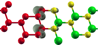
We consider the most primitive set of ion-substitution polar-compensated interfacesHarrison et al. (1978) for the [100] and [111] directions. Figure 1 shows the (111) Si substitution, a (22) polar-compensating substitution of the interface which alters of the atoms in the first plane on the ZnS side of the interface. Other (111) compensations we examine are the Zn substitution for the interface and the Si and S substitutions for the interface. The four substitutions mentioned above can be respectively denoted , , , and , with denoting the “neutral” Si. For the [100] direction we examine the two polar-compensating substitution interfaces having a () interface unit. One interface can be considered either a substitution or a substitution. The other is or .

II.3 Superlattice Potential and Charge
The periodic boundary conditions within a supercell or superlattice are well known to cause artificial bulk electric fields. The piecewise-linear approximation (cf. Ref. Kley and Neugebauer, 1994) of a superlattice potential profile obeys 222 Some degree of approximation, even for , is likely involved in Eq. (1). Replacing the LVP offsets in Eq. (1) with the negatives of the electrostatic potential offsets results in a strictly valid equation for . Unlike the electrostatic potential offsets, the LVP offsets include effects from exchange-correlationWang et al. (2012) and allow charge relaxation effects. the -periodicity relation
| (1) |
along with the the electrostatic relation
| (2) |
Here is the bulk electric field in slab , the interface lies on the side of slab in the positive, or right, direction, and is the jump in the electron LVP going from slab to slab at interface . is the length of slab . is the total (screened) interface charge density at interface . The offsets are considered to be independent of bulk electric fields, and are related to the VBO and conduction band offset (CBO) through the bulk electron affinities and bulk band gaps of the two materials. We typically take the coordinate to be in a direction normal to the interfaces under consideration.
The valence band at one interface cannot be higher than the conduction band at the other interface (except perhaps as allowed by finite size effects). With or without the presence of interface states, which enter the gap and have partial occupations, the potential height change is bounded so that . can often be interpreted as a net charge transfer from a donor interface to an acceptor interface.
II.4 Interface Energies
The sum of the two interface energies and in a two-slab supercell is estimated as
| (3) |
where is the calculated supercell energy and is the number of atoms (or small units such as Zn1S1) of type comprising the cell. is the chemical potential of the constituent . The existence of bulk Si and bulk ZnS provide the constraints , , where is the calculated bulk energy of the material unit , constrained within the cross-section of the supercell. The Zn-rich and Zn-poor conditions are
| (4) | ||||
| (5) |
denotes a calculated zero strain bulk energy; strained bulk energies for Zn and SiS2 are not calculated because the constrained structures are not known. Regardless of growth conditions,
| (6) |
Stoichiometric supercells have and thus do not depend on the growth condition coordinate,
| (7) |
The lack of an intrinsic (bulk) orientation in ZB along the [110] and [100] directions allows two-slab supercells to be constructed so that the two interfaces are mirror images, up to operations in the transverse plane. This generalized mirror symmetry implies , and permits absolute energy calculations. Zinc blende interfaces in general directions, which in this sense includes [111], do not allow a such a construction.Chetty and Martin (1992); Bylander and Kleinman (1988) Individual ZB/ZB and ZB/diamond (111) interface energies do have well defined values333Wurtzite and other structures belonging to 10 particular point groups, have directions in which they do not have unique surface or interface energies.Rapcewicz et al. (1998), but they cannot be determined by total energy calculations using an set of quasi-1D supercell total energies, even allowing for vacuum slabs and slabs of auxiliary materials. As mentioned in Sec. I, there are two methods of calculation: (a) a full 3D calculation of an embedded ZB crystal, such as a tetrahedral crystal with faces (111), (100), (010), and (001), and (b) local energy density methods. In the present work we must be content with interface energies relative to others having the same interface orientation.
II.5 Band Offsets
Typical first principles VBO calculationsVan de Walle and Martin (1987) use the supercell-calculated slab potentials and , and the bulk-calculated quantities and , where is the valence band maximum (VBM) level for slab . The CBO and the LVP offset are then easily obtained using experimental band gaps and electron affinities (for these we use values from Ref. Maierhofer et al., 1991). For ZB (111) interfaces, one encounters the problem that the are not constant in the bulk regions, due to nonzero electric fields . In this case we take the very simple approach of defining nominal interface positions for the relaxed structure, and determine the reference potential offset at interface by linear extrapolation of the potentials. For interface ,
| (8) |
with a similar expression holding for . Here is a position near the center of slab . The potential may be examined using a single or doubleBaroni et al. (1989) convolution smoothing method. We take the nominal interface positions to be midway between the atomic planes that form the interface. (A plane’s position may involve averaging over relaxed ion positions.) In our calculations is the negative of the physical electrostatic potential due to valence charge density and ion core charges.
The extrapolation produces an uncertainty in of approximately
is an estimated width based perhaps on the calculated set of supercell reference potentials . We do not attempt to determine this uncertainty directly, but rely on the a posteriori spread of offset values, having typically four offset calculations per interface. The spread of for a single interface, typically 0.1 to 0.3 eV, is small relative to the range of for different interfaces corresponding to a single direction ( eV). Thus, despite the dipole moment being formally ill-defined for a charged region of space, the extrapolation determined dipoles of well-defined (very small charge) and ill-defined distributions agree rather well.
II.6 Methods of Calculation
The GGA+ method used in our calculations uses the Perdew-Burke-Enzerhof (PBE) GGA functionalPerdew et al. (1996) with a value of eV assigned to the Zn- orbitalsDudarev et al. (1998). This value of both improves the positions of the Zn- bands and the calculated heat of formation of binary Zn compoundsLany (2008). We use the projector augmented wave (PAW) methodBlöchl (1994) as implemented in the code VASPKresse and Furthmüller (1996); *kresse99fro, with the tetrahedral -point occupation methodBlöchl et al. (1994). The bulk permittivity is calculated using density functional perturbation theory.Gonze and Lee (1997)
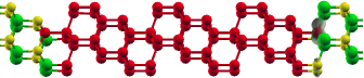
The cross sections of all cells and supercells are determined from the GGA+-relaxed Si structure (calculated lattice parameter Å). For each supercell direction, the corresponding ZnS unit cell is relaxed in the longitudinal direction . The calculated strain in the transverse directions is ( Å). The resulting cross sectional area of the (11) surface units are Å2, Å2, and Å2 for the [110], [100], and [111] directions, respectively. Supercell length can be described by the number of 1D quasi-unit cells in each slab, where a quasi-unit cell is the smallest period for which plane-averaged quantities such as and are repeated in . Supercells444(11) unit cells in both the [110] and [100] directions have two quasi-unit cells and four atoms. We use hexagonal (11) [111] unit cells having three quasi-unit cells and six atoms. having only abrupt interfaces have (11) cross sections while [100] or [111] supercells having at least one defect interface have () or (22) cross sections, respectively. An example of a supercell having polar compensation is shown in Figure 2. The transverse linear -point density is chosen so that (11) [111] and (11) [100] cells have a 1212 -point grid.
We relax all ion positions in each supercell calculation. Fully breaking ion symmetries and/or relaxing supercell length are not done for most calculations, as the effects on energies and offsets are less than 0.1 eV and 0.05 eV, respectively.
The inclusion of the primitive single-substitution defects will allow us to eliminate the abrupt interfaces as stable solutions under most growth conditions. Another benefit of including these polar-compensating defects is the increased number and variety of supercells available for calculation. The resulting spread of electric fields and interface charges aids both offset and energy calculations. Four different systems of equations, each equation (of form Eq. (3)) representing a [100] supercell calculation having , are used to produce four independently calculated absolute energy values for each (100) interface. The same is done with [111] supercells to calculate four independent energy values, relative to or , for each (111) interface. Band offsets are calculated using Eq. (8) for each interface in each supercell calculation.
III Results and Discussion
III.1 Interface Energy Results
The sum of interface energies in each supercell is given in Table 1. The calculated interface energy for the (110) abrupt interface is 2.81 eV/nm2, using .
| , | ||||||||
|---|---|---|---|---|---|---|---|---|
| [110] | ||||||||
| 20 | 0 | 5.61 | ||||||
| [100] | ||||||||
| , | 16 | |||||||
| , | 16 | 2.12 | 0 | |||||
| , | 16 | |||||||
| , | 16 | |||||||
| , | 16 | 0 | ||||||
| , | 16 | |||||||
| , | 16 | 0 | ||||||
| , | 16 | |||||||
| , | 16 | 0 | ||||||
| [111] | ||||||||
| , | 9 | |||||||
| , | 12 | |||||||
| , | 18 | |||||||
| , | 24 | |||||||
| , | 9 | |||||||
| , | 12 | |||||||
| , | 9 | |||||||
| , | 9 | |||||||
| , VL | 12 | |||||||
| , | 9 | |||||||
| , | 12 | |||||||
| , | 9 | |||||||
| , | 9 | |||||||
| , | 9 | |||||||
| , | 12 | |||||||
| , | 9 | |||||||
| , | 9 | |||||||
| , VL | 12 | |||||||
| , | 12 | |||||||
| , | 12 | |||||||
| , | 9 | |||||||
| , | 9 | |||||||
| , | 9 | |||||||
| , | 9 | |||||||
Figure 3 shows the means and the ranges of the calculated interface energies for the [100] direction, as well as the [110] result.
The most stable (100) interfaces are polar-compensated, with the exception (for the set of considered interfaces) of the abrupt cation termination under Zn-rich conditions ( eV/nm2). The calculations also show the interface to be more stable than the (Si-S) interface, for the full range of chemical potential space. This is somewhat unexpected in light of the measurementsMaierhofer et al. (1991); Zhou et al. (1997) discussed in Sec. II.1 which suggest that the (111) Si surface prefers a S adlayer to a Zn adlayer. The fact that the formation of an interfacial SiS2 layer is sensitive to growth environment (Sec. II.1) indicates that the experimental growth conditions in these studies are likely to have been Zn-poor. At these conditions, the interface energy is 7.1 eV/nm2, still less than the energy of 8.4 eV/nm2. However, the calculation suggests a that defective interface such as or is the most stable under the experimental Zn-poor conditions. This result is not in any serious conflict with experimentsMaierhofer et al. (1991); Zhou et al. (1997).
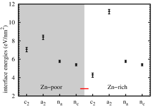
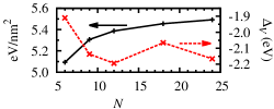
Figure 4 shows the calculated (111) interface energies relative to the abrupt interfaces for both and orientations. Figure 5 demonstrates convergent behavior for in the , supercells with increasing slab size, . The difference between the and calculations is less than 0.2 eV/nm2 despite these supercells having the highest field due to their strong donor-acceptor nature. The calculation of convergence with large in this worst case is preferred to applying electrostatic energy corrections which either require surfaces (additional unknowns) or the assumption of transitivity (see Sec. I).
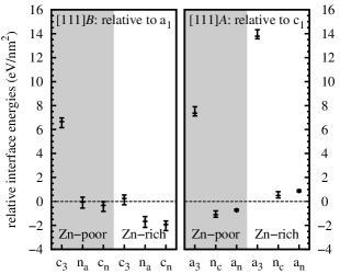
The two considered reconstructions of the interface, and , appear to be stable over nearly the entire range of chemical potential space ( eV). Additionally, the two reconstructions of the interface appear to be stable for over about half of the -space. Both the and interfaces are unstable when compared to the competing, polar-compensated interfaces, and are clearly unlikely to form.
Among the interfaces considered, we have the directional stability relations given by the energy inequalities:
| (9) |
which hold separately for Zn-rich and Zn-poor growth conditions. Appendix A discusses how such energy inequalities must be determined. While it is not possible to show that , we may conclude that , where all energies refer to the same growth conditions.
The calculated directional energy minima and are only upper bounds for experimentally realized minima, which almost certainly involve more complex defect structures and may be growth dependent due to metastable structures. However, we may note that our directional stability relations for Si/ZnS differ somewhat from similar theoretical investigations of type IV/III-V interfaces: studiesLee et al. (1990); Dandrea et al. (1990) of Ge/GaAs, Si/GaAs, and Si/GaP interfaces based on short-period ( to 4) superlattices suggest that, for , is less than .
III.2 Band Offset Results
For the [111] supercell, Figure 6 shows the plane-averaged, doubly convolvedBaroni et al. (1989) electrostatic reference potential and the parallel extrapolations lines used to estimate the values. The two polar interfaces form a donor-acceptor pair resulting in a large charge transfer. The total charge in the Si-S interface region as determined by fields at the slab centers is , while the version of the supercell has charge . These are the largest charge values of all the supercells considered for the calculations of band offsets and interface energies, respectively. Despite the uncertainty in the VBO calculation that is evident from the relatively large fields, the results are within 0.1 eV of a similar calculation having an additional vacuum slab and the charge transfer (Table 1). Figure 5 shows relatively small variation of as is varied. The extrapolation technique demonstrated in Fig. 6 has been used to determine all valence band offset values.
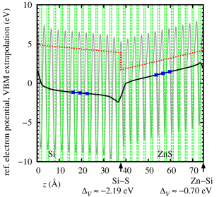
Table 1 shows , , and data from individual supercell calculations. Calculated and experimental results are shown in Figure 7. The (11) [111] supercells used in the data sets have length rather than . The and data sets for each include an supercell having an single interface and a vacuum slab with pseudo-hydrogen terminated surfaces.
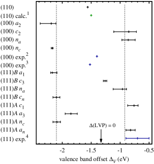
The calculated values vary from about eV to eV. VBOs for both [100] and [111] directions fall into two groups of values, one including all abrupt anion terminations, centered at eV, and the other including all abrupt cation terminations, centered at eV. Our calculated (110) lies near the center of the entire distribution and agrees well with Li et al.Li et al. (1996) The experimental valuesBrar and et al (1997); Lew Yan Voon et al. (1997) for the [100] direction also lies near the average of the two groups. The simplest interface structures expected to have interface dipoles this small are 50/50 mixtures of and substitutions.
In contrast to the other experimental results, the (111) VBO of Maierhofer et al.Maierhofer et al. (1991) lies clearly in a single group (the abrupt cation group). This indicates that the grown macroscopic (111) interfaces in these experiments had significant selectivity among the possible microscopic interfaces.
The bimodal behavior of the offsets calculated here can be grossly explained by a two charge model. For anion terminated polar interfaces with electronic compensation, the extra electrons will go into a localized anti-bonding state formed primarily from Si and ZnS conduction bands. The conduction band minimum (CBM) on the Si side is lower than the CBM on the ZnS side, and thus the electrons localize preferentially on the Si side of the interface. (For the interface in simulations with and without ion relaxation, the center of mass of the occupied portion of the Si-S interface state (Figure 8) can be verified by inspection of the to lie on the bulk side of the interfacial Si atomic plane.Note (1)) A cation terminated polar interface has extra holes which also preferentially localize on the Si side of the interface, due to its higher VBM. In the large limit, the free charge approaches the magnitude of the compositional charge, but with opposite sign, forming a dipole. The location of the compositional charge is not well defined. In particular, starting as in Harrison et al.Harrison et al. (1978) with the insulating “frozen bulk” electronic state of Si on both sides of the interface (all Zn and S nuclei being created by transferring protons between adjacent Si atoms in one half plane), one can interpret the positive compositional charge at a Si-S interface as being generated by either the S or Si ion cores. This symmetric situation can be modeled by placing the compositional charge at the center of the interface bond region. Having compositional charge near the bond center and the free charge first moment located outside of the central bond region yields, for all abrupt polar interfaces, the correct sign of the dipoles and (LVP) values (Fig. 7).
Dipoles at ionically compensated interfaces can be analyzed in terms of changes to the electronically compensated abrupt interfaces. The substituting nuclei can be constructed by moving the free charges into nuclei of the abrupt interface. This construction changes electronic reconstruction into ionic reconstruction. Within the model above, we may form a rule that the dipole changes sign if the free charge crosses the interface as it moves into the nuclei. This rule can be seen to place each polar-compensating (100) and (111) interface shown in Fig. 7 onto the correct side of the distribution.
Alternatively, one may first determine the sign of the dipoles of the polar compensated interfaces using the arguments of Harrison et al.Harrison et al. (1978), and secondly determine the dipoles of the abrupt interfaces by moving charge out of the substituting nuclei.
The two charge model creates the type of dipole switching necessary to create the bimodal distribution. However, the model ignores the important screening effect of the valence electrons on the dipoles. With screening suppressed, the locations of the free charge component and the bond-centered compositional charge suggest abrupt interface dipole densities greater than 0.5 Å. In contrast, the interface dipole densities corresponding to the (LVP) values of the left and right distribution peaks in Fig. 7 are Å and Å per [111] surface unit, respectively. We find that this reduction in by an order of magnitude persists at fixed ion interfaces, indicating the predominant screening comes from electrons in the interface region.
While the two charge model contains the dipole behavior necessary for a bimodal distribution, there may not exist a single explanation for the relative narrowness of the two peaks. The offsets for the triple bond interfaces and are clearly moved toward the center, reflecting that they have a different bonding geometry and atomic plane spacing than the remaining single bond [111] interfaces. If common bonding geometry is a unifying factor, the very close agreement of the four double bond interfaces ([100] direction) with the six single bond interfaces may be somewhat coincidental.
The (110) VBO lies near the center of the distribution. This is expected as non-polar interface offsets are typically close to a mean or “bulk” offset value that exists independent of interface direction or details. Highly non-uniform interfaces may be best handled with calculations in non-polar directions, or the use of direction-independent junction models such as that of of MönchMönch (2007). In contrast to this “bulk picture” result is the large width (1.2 eV) of the entire offset distribution and the fact that grown interfacesMaierhofer et al. (1991) can lie on a single peak. The most transparent violations of the transitivity rule comes from the cation and anion terminated supercells, for which the opposing interface band offsets differ by 0.55 and 0.38 eV respectively (see Table 1). It is clear that the need to treat each interface individually will increase as high quality interfaces become more common.
Finally, it is a worthwhile exercise to consider the band offset results in light of the experiments by Maierhofer et al.Maierhofer et al. (1991) for (111) interfaces. Among the interfaces considered here there are three potentially stable (111) candidates having acceptable offsets: , , and . As noted in Sec. II.1, Maierhofer et al.Maierhofer et al. (1991) suggests that the first layer of ZnS in [111] growth is primarily , lowering the likelihood of the and interfaces. When ZnS is deposited on a cleaved (21) (111) Si surface, as is done by Maierhofer et al., the formation of an interface seems unlikely because it would involve either the presence extra Si atoms on the surface, or removing seven out of eight Si atoms in the first bilayer to achieve the effect of a Si substitution into ZnS. It is perhaps most probable that the experiment created interfaces that are not formed from the primitive substitutions considered here. As mentioned previously however, the non-bulk dipole signifies a degree of selectivity within the universe of low energy microscopic interface structures.
IV Conclusions
Polar interfaces of traditional semiconductors contain the physical ingredients needed to produce the carrier and charge phenomena now commonly examined in complex oxide structures. Any compositional (polar) charge between slabs of sufficient thickness must be screened by induced bound charge, conventional polarization charge (e.g. piezoelectric charge), and free charge. Induced bound charge and net charge go to zero as , while the remaining components generally reach non-zero asymptotes. The most stable interfaces are almost always polar-compensated, containing no compositional charge and generally lacking the need for any free charge. For this reason the predicted metallicity in semiconductor abrupt polar interfaces is avoided, as it is in most oxide interfaces.
The closely lattice matched Si/ZnS interfaces deserve investigation for both practical and theoretical reasons. The enthalpy studies here confirm that polar-compensated interfaces are typically more stable than abrupt interfaces. In the polar [100] direction, only the abrupt Si-Zn interface under Zn-rich conditions has not been excluded by the set of primitive (single-substitution) polar-compensating defects considered here. In the [111] direction, interfaces having three interface bonds per interface atom are clearly unstable under all conditions, and this is likely also true for interfaces with one interface bond per atom.
The band offset calculations performed here show that the abrupt and single-substitution polar-compensated (100) and (111) interfaces have a bimodal distribution of offsets, with peaks at VBO values of eV and eV. The width of the distribution indicates that band offset transitivity is violated by over 1.2 eV. The Si-Zn interfaces having (111) (single bond) and (111) (triple bond) orientations have a VBO difference of 0.5 eV, indicating that interface orientation plays nearly as large a role as the ionic character of an interface. A measured (111) VBO valueMaierhofer et al. (1991) lies near the peak at eV and shows a clear preference of interface dipole. Measured (100) VBO valuesBrar and et al (1997); Lew Yan Voon et al. (1997) correspond with the average value of the distribution, and indicate the presence of ordered or disordered polar compensating structures having no net dipole. The existence of the bimodal interface dipole distribution is consistent with a primitive two charge model considering the free charge and the compositional charge.
Finally we have shown that extrapolation of linearly varying potentials can produce band offsets that are consistent with supercell calculations involving negligible electric fields . Furthermore, interface energy calculations calculated using cells with significant fields and interface charges are consistent with energy calculations using only low supercells. Nine or more atomic bilayers per slab provides adequate length for meaningful results.
Acknowledgements.
This work has been supported by the National Science Foundation of the USA under Grant SOLAR DMS-1035513.Appendix A Directional Energies
Here we note how energy inequalities such as Eq. (9) must be computed, assuming a given set of defective interfaces. In the statement , simply denotes the minimum computed (100) interface energy. For the [111] direction however, algebraic considerations yield an uncertainty in for interfaces and having respective orientations and . Since is unknown, we must assume that its actual value may hinder the inequality we wish to state. We first determine the maximum of , with respect to the . This maximum occurs at and thus the candidate value for for this and is . Minimizing over interface pairs, the appropriate value is given in terms of calculable values as . For our set of interfaces, is and eV/nm2 for Zn-poor and Zn-rich conditions, respectively. One cannot establish for any direction because the appropriate for this inequality involves a minimum with respect to , rather than a maximum; here must be allowed to go to its lowest possible value, zero (excluding negative interface energies). It follows that for two general directions, no directional energy inequality may be written without using an alternate means of interface energy computation (see Sec. I).
References
- Goniakowski et al. (2008) J. Goniakowski, F. Finocchi, and C. Noguera, Reports on Progress in Physics 71, 016501 (2008).
- Chambers et al. (2010) S. Chambers, M. Engelhard, V. Shutthanandan, Z. Zhu, T. Droubay, L. Qiao, P. Sushko, T. Feng, H. Lee, T. Gustafsson, E. Garfunkel, A. Shah, J. Zuo, and Q. Ramasse, Surface Science Reports 65, 317 (2010).
- Moetakef et al. (2011) P. Moetakef, T. A. Cain, D. G. Ouellette, J. Y. Zhang, D. O. Klenov, A. Janotti, C. G. V. d. Walle, S. Rajan, S. J. Allen, and S. Stemmer, Applied Physics Letters 99, 232116 (2011).
- Huang et al. (2012) B.-C. Huang, Y.-P. Chiu, P.-C. Huang, W.-C. Wang, V. T. Tra, J.-C. Yang, Q. He, J.-Y. Lin, C.-S. Chang, and Y.-H. Chu, Physical Review Letters 109, 246807 (2012).
- Baraff et al. (1977) G. A. Baraff, J. A. Appelbaum, and D. R. Hamann, Physical Review Letters 38, 237 (1977).
- Harrison et al. (1978) W. A. Harrison, E. A. Kraut, J. R. Waldrop, and R. W. Grant, Physical Review B 18, 4402 (1978).
- Kley and Neugebauer (1994) A. Kley and J. Neugebauer, Physical Review B 50, 8616 (1994).
- Bernardini and Fiorentini (1998) F. Bernardini and V. Fiorentini, Physical Review B 57, R9427 (1998).
- Leitsmann et al. (2006) R. Leitsmann, L. E. Ramos, and F. Bechstedt, Physical Review B 74, 085309 (2006).
- Stengel (2011) M. Stengel, Physical Review Letters 106, 136803 (2011).
- Ohtomo and Hwang (2004) A. Ohtomo and H. Y. Hwang, Nature 427, 423 (2004).
- Maierhofer et al. (1991) C. Maierhofer, S. Kulkarni, M. Alonso, T. Reich, and K. Horn, Journal of Vacuum Science & Technology B: Microelectronics and Nanometer Structures 9, 2238 (1991).
- Romano et al. (1995) L. T. Romano, R. D. Bringans, X. Zhou, and W. P. Kirk, Physical Review B 52, 11201 (1995).
- Zhou et al. (1997) X. Zhou, S. Jiang, and W. P. Kirk, Journal of Applied Physics 82, 2251 (1997).
- Shen and Kwok (1994) W. P. Shen and H. S. Kwok, Applied Physics Letters 65, 2162 (1994).
- Wei and Choy (2002) M. Wei and K.-L. Choy, Chemical Vapor Deposition 8, 15–17 (2002).
- Tran and Lamb (2002) N. H. Tran and R. N. Lamb, The Journal of Physical Chemistry B 106, 352 (2002).
- Lee et al. (2003) E. Y. M. Lee, N. H. Tran, J. J. Russell, and R. N. Lamb, The Journal of Physical Chemistry B 107, 5208 (2003).
- Yu et al. (2013) Y. Yu, Y. Jiang, P. Jiang, Y. Zhang, D. Wu, Z. Zhu, Q. Liang, S. Chen, Y. Zhang, and J. Jie, Journal of Materials Chemistry C 1, 1238 (2013).
- Mastio et al. (2001) E. A. Mastio, W. M. Cranton, and C. B. Thomas, Journal of Applied Physics 89, 1605 (2001).
- Xu and Li (2009) H. J. Xu and X. J. Li, Semiconductor Science and Technology 24, 075008 (2009).
- Hsiao et al. (2013) Y. J. Hsiao, T. H. Meen, L. W. Ji, J. K. Tsai, Y. S. Wu, and C. J. Huang, Journal of Physics and Chemistry of Solids 74, 1403 (2013), WOS:000322351400011.
- Wang et al. (2012) W. Wang, J. Shao, and Z. Li, Chemical Physics Letters 522, 83 (2012).
- Rapcewicz et al. (1998) K. Rapcewicz, B. Chen, B. Yakobson, and J. Bernholc, Physical Review B 57, 7281 (1998).
- Chetty and Martin (1992) N. Chetty and R. M. Martin, Physical Review B 45, 6089 (1992).
- Bylander and Kleinman (1988) D. M. Bylander and L. Kleinman, Physical Review B 38, 7480 (1988).
- Dandrea et al. (1990) R. G. Dandrea, S. Froyen, and A. Zunger, Physical Review B 42, 3213 (1990).
- Mankefors (1999) S. Mankefors, Physical Review B 59, 13151 (1999).
- Leitsmann and Bechstedt (2007) R. Leitsmann and F. Bechstedt, Physical Review B 76, 125315 (2007).
- Brar and et al (1997) B. Brar and et al, in Compound semiconductors 1997 (San Diego, CA, 1997).
- Li et al. (1996) K.-h. Li, M.-c. Huang, and R.-z. Wang, Chinese Physics Letters 13, 458 (1996).
- Vanderbilt and King-Smith (1993) D. Vanderbilt and R. D. King-Smith, Physical Review B 48, 4442 (1993).
- King-Smith and Vanderbilt (1993) R. D. King-Smith and D. Vanderbilt, Physical Review B 47, 1651 (1993).
- Note (1) For the abrupt stoichiometric [111] superlattice having interface bonds along [111], nearly all non-empty calculated states have either very strong localization or negligible amplitude at the donor interface. The apparent thinness of the shells of -space in which hybridization might be observable may be due to the fact that the apparent crossings of the donor interface state band all lie relatively close to (within 30% of the 2D Brillouin zone effective radius) where the supercell Hamiltonian has significant symmetry . The lack of hybridization is noted at -point densities as high as and is aided by using the tetrahedral method of -point smearing.
- Bringans and Olmstead (1989) R. D. Bringans and M. A. Olmstead, Physical Review B 39, 12985 (1989).
- Weser et al. (1987) T. Weser, A. Bogen, B. Konrad, R. D. Schnell, C. A. Schug, and W. Steinmann, in Proceedings of the 18th International Conference on the Physics of Semiconductors, edited by O. Engstrom (World Scientific, Singapore, 1987) pp. 97–100.
- Jedrzejek et al. (1995) C. Jedrzejek, J. Konior, and S. Kaprzyk, Acta Physica Polonica A 87, 349 (1995), WOS:A1995QN41100012.
- Lew Yan Voon et al. (1997) L. C. Lew Yan Voon, L. R. Ram-Mohan, and R. A. Soref, Applied Physics Letters 70, 1837 (1997).
- Wang (1996) E. Wang, Applied Surface Science 104–105, 626 (1996).
- Laref et al. (2006) A. Laref, S. Laref, B. Belgoumene, B. Bouhafs, A. Tadjer, and H. Aourag, Journal of Applied Physics 99, 043702 (2006).
- Rhim et al. (2009) S. H. Rhim, R. Saniz, and A. J. Freeman, Physical Review B 79, 045313 (2009).
- Note (2) Some degree of approximation, even for , is likely involved in Eq. (1). Replacing the LVP offsets in Eq. (1) with the negatives of the electrostatic potential offsets results in a strictly valid equation for . Unlike the electrostatic potential offsets, the LVP offsets include effects from exchange-correlationWang et al. (2012) and allow charge relaxation effects.
- Note (3) Wurtzite and other structures belonging to 10 particular point groups, have directions in which they do not have unique surface or interface energies.Rapcewicz et al. (1998).
- Van de Walle and Martin (1987) C. G. Van de Walle and R. M. Martin, Physical Review B 35, 8154 (1987).
- Baroni et al. (1989) S. Baroni, R. Resta, A. Baldereschi, and M. Peressi, in Spectroscopy of Semiconductor Microstructures, edited by G. Fasol, A. Fasolino, and P. Luglu (Plenum Press, New York, 1989) pp. 251–271.
- Perdew et al. (1996) J. P. Perdew, K. Burke, and M. Ernzerhof, Physical Review Letters 77, 3865 (1996).
- Dudarev et al. (1998) S. L. Dudarev, G. A. Botton, S. Y. Savrasov, C. J. Humphreys, and A. P. Sutton, Physical Review B 57, 1505 (1998).
- Lany (2008) S. Lany, Physical Review B 78, 245207 (2008).
- Blöchl (1994) P. E. Blöchl, Physical Review B 50, 17953 (1994).
- Kresse and Furthmüller (1996) G. Kresse and J. Furthmüller, Physical Review B 54, 11169 (1996).
- Kresse and Joubert (1999) G. Kresse and D. Joubert, Phys. Rev. B 59, 1758 (1999).
- Blöchl et al. (1994) P. E. Blöchl, O. Jepsen, and O. K. Andersen, Phys. Rev. B 49, 16223 (1994).
- Gonze and Lee (1997) X. Gonze and C. Lee, Physical Review B 55, 10355 (1997).
- Note (4) (11) unit cells in both the [110] and [100] directions have two quasi-unit cells and four atoms. We use hexagonal (11) [111] unit cells having three quasi-unit cells and six atoms.
- Lee et al. (1990) S. Lee, D. M. Bylander, and L. Kleinman, Physical Review B 41, 10264 (1990).
- Mönch (2007) W. Mönch, Applied Physics Letters 91, 042117 (2007).