Sub-gap spectroscopy of thermally excited quasiparticles in a Nb contacted carbon nanotube quantum dot
Abstract
We present electronic transport measurements of a single wall carbon nanotube quantum dot coupled to Nb superconducting contacts. For temperatures comparable to the superconducting gap peculiar transport features are observed inside the Coulomb blockade and superconducting energy gap regions. The observed temperature dependence can be explained in terms of sequential tunneling processes involving thermally excited quasiparticles. In particular, these new channels give rise to two unusual conductance peaks at zero bias in the vicinity of the charge degeneracy point and allow to determine the degeneracy of the ground states involved in transport. The measurements are in good agreement with model calculations.
pacs:
73.23.Hk, 73.63.Kv, 74.45.+cIntroduction– Carbon nanotubes (CNTs) are highly versatile quantum systems, whose properties can be investigated by attaching them to a wide variety of different contact materials.Bockrath et al. (1997); Jensen et al. (2005); Kasumov et al. (2003) By using superconducting metals as electrodes, a significant increase of spectroscopic resolution due to the sharp peaks at the gap edges in the BCS density of states can be achieved.Grove-Rasmussen et al. (2009) Depending on the coupling strength between the carbon nanotube and its leads, the nanotube can act as a Josephson weak link, and proximity-induced supercurrent can flow through the quantum dot.Kasumov et al. (2003); Cleuziou et al. (2006); Jarillo-Herrero et al. (2006); Pallecchi et al. (2008) The supercurrent is carried by Andreev bound states, whose presence is revealed by peculiar subgap features.Dirks et al. (2011); Pillet et al. (2010); Kim et al. (2013); Pillet et al. (2013); Kumar et al. (2014) By fabricating the contacts from sputtered Nb, they can remain superconducting up to a critical temperature and a correspondingly large critical magnetic field .
In this work we report on sub-gap features observed in a CNT quantum dot weakly coupled to superconducting leads. Strikingly, such features are not visible at the lowest temperatures achieved in the experiment but only when the temperature becomes comparable to the superconducting gap. This suggests that, as explained below, the observed sub-gap features are not due to Andreev reflections but rather to thermal excitation of quasiparticles across the gap, as predicted recently by some of us.Pfaller et al. (2013) We perform a systematic analysis of the temperature dependence of the observed features. A good agreement between experimental data and theoretical predictions in the linear as well as in the nonlinear regime is obtained.
Experimental details– The measurements presented here were performed on a single wall carbon nanotube grown by chemical vapour deposition (CVD).Kong et al. (1998) As substrate highly p-doped Si capped with is used. The electrodes to the nanotube are composed of Pd as contact layer and sputtered Nb with a contact spacing of the order of . The room temperature resistance of our device is in the range of .
For performing two- and four-point measurements, each superconducting electrode is connected to two AuPd leads as resistive on-chip elements that are, among other filter stages, supposed to damp oscillations at the plasma frequency of the Josephson junction.Martinis and Kautz (1989); Pallecchi et al. (2008)
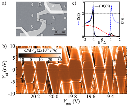
A scanning electron micrograph of the sample is shown in Fig. 1(a). The device was measured in a dilution refrigerator with a base temperature of .
Transport spectroscopy– Fig. 1(b) shows an overview plot of the differential conductance as a function of source-drain voltage and gate voltage at . This temperature is much smaller than the critical temperature expected for our Nb contacts. The measurement of Fig. 1(b) serves as a reference for the high temperature experiments and theoretical predictions discussed below. Besides regular Coulomb diamonds, a rich substructure of both elastic and inelastic cotunneling lines is observed,De Franceschi et al. (2001); Grove-Rasmussen et al. (2009); Holm et al. (2008) reflecting the high spectroscopic resolution brought about by the sharp peaks in the BCS density of states (cf. Fig. 1(c)).
The superconducting energy gap estimated from the sequential tunneling features at (see details below) is , compared to an expected value of for bulk Nb.111An evaluation of the elastic cotunneling lines in Fig. 1(b), not within the scope of our lowest-order theory, results in a slightly reduced value . This reduction of the gap has been reported before in similar Nb-based devices.Grove-Rasmussen et al. (2009); Kumar et al. (2014) Its origin so far remains an open question, though contamination of the lower Nb interface, formation of niobium oxideHulm et al. (1972), or the thin Pd contact layer may play a role.Grove-Rasmussen et al. (2009) Estimated from , the resulting effective critical temperature would be . However, features in the data attributable to superconductivity remain present up to temperatures of about , and measurements of a co-deposited Nb strip of comparable dimensions on the same chip yielded a critical temperature of .
From additional stability diagrams similar to Fig. 1(b) but taken at higher temperatures and finite magnetic field to suppress superconductivity (not shown), we estimate a charging energy . From the fitting between experiments and theory discussed below (cf. in particular Eq. (4)), a coupling strength between quantum dot and leads of is extracted. This places our measurement into the parameter range where Coulomb repulsion dominates transport, superconductivity enhances the spectroscopic resolution, De Franceschi et al. (2010) and Andreev reflections are expected to be strongly suppressed.Buitelaar et al. (2003) No obvious traces of Kondo phenomena Goldhaber-Gordon et al. (1998) are observed neither in the normal nor in the superconducting state.
Thermally activated transport– For quantum dots connected to superconducting leads, transport is usually blocked in the energy gap range . At high temperature, transport becomes possible both at low bias and in parts of the Coulomb blockade region due to quasiparticles excited across the superconducting energy gap.Pfaller et al. (2013) This is illustrated in Fig. 1(c), showing the product (black solid line) of the quasiparticle density of states (blue dash-dotted line) and the Fermi function (red dotted line). For sufficiently high temperature, corresponding to a thermal broadening of the Fermi function of the order of the gap, a small peak at emerges. This peak vanishes at low temperature when the broadening of the Fermi function is much smaller than the gap. The focus of this work is the systematic investigation of features due to this extra thermal channel, both from the theoretical and experimental point of view. In the following we distinguish between standard resonance lines, which are also present at low temperatures, and thermal lines due to the presence of the extra thermal peak.
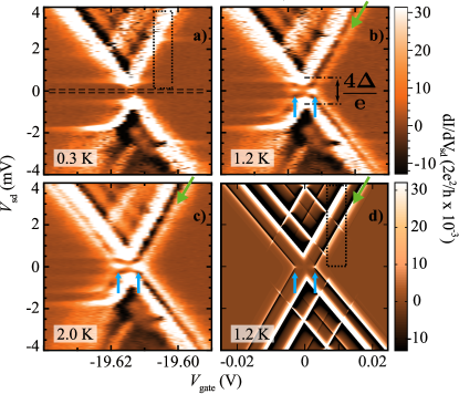
Fig. 2(a)-(c) displays detailed measurements of the differential conductance at increasing temperatures, close to the charge degeneracy point marked by the black rectangle in Fig. 1(b). 222An apparent discrepancy in gate voltage range between Fig. 1(b) and Fig. 2(a)-(c) is due to long-time scale uniform drift of all Coulomb blockade features. The conductance peaks have been re-identified from overview measurements. The comparison of Fig. 2(a) and Figs. 2(b) and (c) gives direct evidence that at temperatures above additional transition lines parallel to the sequential tunneling lines emerge within the region of Coulomb blockade, see e.g. the green arrow in Fig. 2(b)-(d). These lines are separated from the sequential tunneling lines by a characteristic region of negative differential conductance (NDC, dark). As can be seen in Fig. 2(d), the additional lines and the NDC regions are reproduced by our transport calculations described in detail below, which account for sequential tunneling processes of thermally excited quasiparticles. At the intersection of such lines we obtain two zero bias conductance peaks indicated by blue arrows and separated by , with as the gate coupling factor.
Theoretical model– Our calculations are based on a master equation approach for the reduced density matrix (RDM) to lowest order in the tunneling to the leads, including only quasiparticle tunneling.Pfaller et al. (2013) The theory is generalized here to include also the shell and orbital degrees of freedom of the CNT. Specifically, the quantum dot is modeled by the Hamiltonian
| (1) |
where is a collective quantum number accounting for longitudinal and orbital degrees of freedom, respectively, and labels the spin. 333The term longitudinal mode is referring to the energy quantization associated to the finite length of the carbon nanotube. The Hamiltonian in Eq. (1) includes both spin orbit interaction and KK’ mixing terms. Since it is written in the diagonal basis, the quantum number is accounting for the “orbital” degrees of freedom, which are linear combinations of states in the basis. Flensberg and Marcus (2010) Finally, we employ a constant interaction model for the Coulomb repulsion on the tube with strength . Including two longitudinal modes, , and accounting for the two orbital degrees of freedom, , of the CNTs, represents four energy levels with energies , , , and . The characteristic fourfold degeneracy of the carbon nanotube spectrum is assumed to be lifted by originating from spin orbit splitting and valley-mixing .Flensberg and Marcus (2010)
The size of the experimentally measured Coulomb diamonds and the positions of the excited state lines in the stability diagrams are consistent with the assumption that the transitions occur between states with and electrons. They are correctly reproduced in our model with , a spacing between the longitudinal modes , and . The gate voltage is assumed to linearly shift the single particle energy levels . At finite bias voltage the electrochemical potentials in the source and drain electrodes are , where and account for the asymmetric bias drop at the source and drain contact, respectively. From our simulations, we find an effective back gate coupling and an asymmetric bias drop .
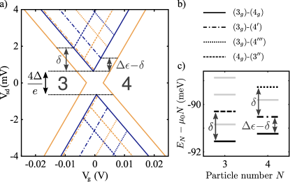
The expected positions of the differential conductance lines of the stability diagrams are displayed in Fig. 3(a). The solid blue lines show the electron ground state to electron ground state transition -, the broken blue lines are instead transition lines between a ground state and an excited state of the neighbouring particle number, see Fig. 3(b). Each of the possible standard transition lines is accompanied by an associated thermal line (in orange, same line style) due to thermally activated quasiparticles. We set the zero of the gate voltage at the charge degeneracy point. The position of the blue transition lines is then dictated by the standard sequential tunneling requirements,Pfaller et al. (2013)
| (2) |
for source lines () and drain () lines. Here, is the energy difference between an excited state and a ground state with the same particle number in the many-body spectrum of Fig. 3(c). In the case of a source (drain) transition is calculated in the () particle subspace. For a ground state to ground state transition, in Eq. (2).
The conditions for the occurrence of an orange thermal line are
| (3) |
Thus, each replica runs parallel to the diamond edge at a distance from the standard line associated to it.
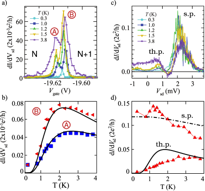
Low bias conductance– Fig. 4(a) shows the gate voltage dependence of the low bias differential conductance for increasing temperature. Each trace is an average of several measurements taken at small but finite bias values symmetrically located around and corresponding to the area between the dashed horizontal lines in Fig. 2(a). Note that due to the existence of a superconducting energy gap, no current would be expected in this bias voltage range. Two clearly distinguishable peaks are observed. They result from the zero-bias crossing of the thermally induced transition lines. Due to their thermal nature, they decrease for decreasing temperature. At the double peak is absent. A single peak observed at approximately the position of the charge degeneracy point may be due to higher order processes not captured by the theory discussed below.
In Fig. 4(b) the maximal conductance measured at the two peaks denoted by A and B in Fig. 4(a) is plotted as a function of the temperature (squares and triangles, respectively). The observed behaviour is well reproduced by an analytic expression for the linear conductance derived around the to charge degeneracy point (solid lines). By taking into account the ground state energy levels of the relevant and -particles subspace, we find
| (4) |
with the BCS density of states , and the occupation probability of the -particle ground state . The energy difference between the two ground states scales linearly with and equals zero at the charge degeneracy point. Here, is a phenomenological Dynes parameterDynes et al. (1978) related to a finite lifetime of the quasiparticles in the superconducting leads. The Dynes parameter is introduced to renormalize the BCS density of states and therefore leads to a broadening of the conductance peaks. Eq. (4) predicts the existence of two maxima of the conductance located symmetrically around . The values of the maxima as a function of the temperature correspond to the two solid lines in Fig. 4(b).
We notice a good agreement between experiment and theory at temperatures above . From the fit we extract the coupling parameter and the Dynes parameter . The temperature dependence of the conductance peaks can be divided into two regimes. At low temperature, i.e., in the thermal activation regime, the “” term of Eq. (4) dominates, leading to a steep increase of the peaks with temperature. In the high temperature regime, we see the typical decay known from standard sequential tunneling processes.Beenakker (1991)
Of particular interest is the ratio of the conductance maxima of the left and the right peak. Since Eq. (4) is symmetric around , we find that the ratio is equal to
| (5) |
where canonical expressions were used for the occupation probabilities and , and () denotes the degeneracy of the and particles ground state. Thus, it is possible to directly probe the degeneracy of the two ground states using Eq. (5). Fig. 4(a) and (b) show that the conductance at point (B) is larger than at point (A), leading to the conclusion that the -particles ground state has a larger degeneracy than the -particles ground state. This confirms the assumption that the data are measured around a - type charge degeneracy point, as also supported by the correspondence between the theory and experiment of excited state transition lines (see Fig. 2).
According to our model, the four fold degeneracy of the CNT is broken and the degeneracy of a ground state with odd number of particles, due to time reversal symmetry, equals . Taking the ratio of the measured peak height of the two thermally induced conductance peaks provides, to our knowledge, a new method to determine the degeneracy of the ground state of multi-electron quantum dot single electron transistors.
Finite bias conductance– The behavior of thermal and standard transitions at finite bias is depicted in Fig. 4(c), which shows traces at various temperatures. These traces result from an average taken over the voltage range marked by the dotted box in Fig. 2(a).444In order to not introduce an artificial broadening in the average, since the conductance peaks lie at different for different values of , the curves were shifted to compensate for that offset. The reference with respect to which all other curves were shifted was always the curve closest to the degeneracy point. Repeating that procedure for different temperatures yields Fig. 4(c). We observe two peaks which evolve in opposite ways at increasing temperature: the standard peak (s.p.) at higher decreases as expected from standard sequential tunneling.Beenakker (1991) The second one at lower increases and hence confirms thermally assisted quasiparticle tunneling (thermal peak, th.p.). A characteristic dip evolving into NDC is also clearly observed in the line traces in Fig. 4(c).
In Fig. 4(d) the extracted temperature dependence of both the thermally activated and the standard sequential tunneling peak is depicted (triangles). Similar to the data analysis of the experiments, also the theoretical curves for the peak height were calculated via averaging over the voltage range marked with the dotted rectangle in Fig. 2(d). Our perturbative theory is overestimating the height of the standard peak. Hence, the theoretical curve (dash-dotted line) was multiplied by to allow a better comparison with experimental data. A decrease of the peak is observed with increasing temperature. The calculation for the thermally activated peak (solid black line) is in good agreement with experiments; it shows a similar temperature dependence as the conductance peaks in Fig. 4(b).
Preliminary calculations show that a renormalization of the lowest order theory taking into account also charge fluctuations in the framework of a dressed second order theoryKern and Grifoni (2013) can reproduce the broadening (linewidth) of the resonance peaks and gives the correct ratio between the peak height of the thermally induced and the standard sequential tunneling peak. This study will be the subject of an upcoming publication.
Conclusions– We demonstrate thermally activated quasiparticle transport in a carbon nanotube quantum dot with superconducting contacts. Our theoretical analysis shows that the new lines in the otherwise blockaded regions of the stability diagram appear already in the sequential tunneling regime. The splitting of the thermally induced conductance peaks at low bias can be used to probe the degeneracy of the ground states, and provides a particularly useful method to determine charge configurations from transport characteristics.
The authors would like to thank Kicheon Kang for insightful discussions. We acknowledge funding from the Deutsche Forschungsgemeinschaft (SFB 631 TP A11, GRK 1570, Emmy Noether project Hu 1808-1) and from the EU FP7 Project SE2ND.
References
- Bockrath et al. (1997) M. Bockrath, D. H. Cobden, P. L. McEuen, N. G. Chopra, A. Zettl, A. Thess, and R. E. Smalley, Science 275, 1922 (1997).
- Jensen et al. (2005) A. Jensen, J. R. Hauptmann, J. Nygård, and P. E. Lindelof, Phys. Rev. B 72, 035419 (2005).
- Kasumov et al. (2003) A. Kasumov, M. Kociak, M. Ferrier, R. Deblock, S. Guéron, B. Reulet, I. Khodos, O. Stéphan, and H. Bouchiat, Phys. Rev. B 68, 214521 (2003).
- Grove-Rasmussen et al. (2009) K. Grove-Rasmussen, H. I. Jørgensen, B. M. Andersen, J. Paaske, T. S. Jespersen, J. Nygård, K. Flensberg, and P. E. Lindelof, Phys. Rev. B 79, 134518 (2009).
- Cleuziou et al. (2006) J.-P. Cleuziou, W. Wernsdorfer, V. Bouchiat, T. Ondarcuhu, and M. Monthioux, Nat. Nanotech. 1, 53 (2006).
- Jarillo-Herrero et al. (2006) P. Jarillo-Herrero, J. A. van Dam, and L. P. Kouwenhoven, Nature 439, 953 (2006).
- Pallecchi et al. (2008) E. Pallecchi, M. Gaass, D. A. Ryndyk, and C. Strunk, Appl. Phys. Lett. 93, 072501 (2008).
- Dirks et al. (2011) T. Dirks, T. L. Hughes, S. Lal, B. Uchoa, Y.-F. Chen, C. Chialvo, P. M. Goldbart, and N. Mason, Nat. Phys. 7, 386 (2011).
- Pillet et al. (2010) J.-D. Pillet, C. H. L. Quay, P. Morfin, C. Bena, A. L. Yeyati, and P. Joyez, Nat. Phys. 6, 965 (2010).
- Kim et al. (2013) B.-K. Kim, Y.-H. Ahn, J.-J. Kim, M.-S. Choi, M.-H. Bae, K. Kang, J. S. Lim, R. López, and N. Kim, Phys. Rev. Lett. 110, 076803 (2013).
- Pillet et al. (2013) J.-D. Pillet, P. Joyez, R. Žitko, and M. F. Goffman, Phys. Rev. B 88, 045101 (2013).
- Kumar et al. (2014) A. Kumar, M. Gaim, D. Steininger, A. Levy Yeyati, A. Martín-Rodero, A. K. Hüttel, and C. Strunk, Phys. Rev. B 89, 075428 (2014).
- Pfaller et al. (2013) S. Pfaller, A. Donarini, and M. Grifoni, Phys. Rev. B 87, 155439 (2013).
- Kong et al. (1998) J. Kong, H. Soh, A. Cassell, C. Quate, and H. Dai, Nature 395, 878 (1998).
- Martinis and Kautz (1989) J. M. Martinis and R. L. Kautz, Phys. Rev. Lett. 63, 1507 (1989).
- De Franceschi et al. (2001) S. De Franceschi, S. Sasaki, J. M. Elzerman, W. G. van der Wiel, S. Tarucha, and L. P. Kouwenhoven, Phys. Rev. Lett. 86, 878 (2001).
- Holm et al. (2008) J. V. Holm, H. I. Jørgensen, K. Grove-Rasmussen, J. Paaske, K. Flensberg, and P. E. Lindelof, Phys. Rev. B 77, 161406 (2008).
- Note (1) An evaluation of the elastic cotunneling lines in Fig. 1(b), not within the scope of our lowest-order theory, results in a slightly reduced value .
- Hulm et al. (1972) J. K. Hulm, C. K. Jones, R. A. Hein, and J. W. Gibson, Journal of Low Temperature Physics 7, 291 (1972).
- De Franceschi et al. (2010) S. De Franceschi, L. Kouwenhoven, C. Schönenberger, and W. Wernsdorfer, Nat. Nanotech. 5, 703 (2010).
- Buitelaar et al. (2003) M. Buitelaar, W. Belzig, T. Nussbaumer, B. Babić, C. Bruder, and C. Schönenberger, Phys. Rev. Lett. 91, 057005 (2003).
- Goldhaber-Gordon et al. (1998) D. Goldhaber-Gordon, J. Göres, M. A. Kastner, H. Shtrikman, D. Mahalu, and U. Meirav, Phys. Rev. Lett. 81, 5225 (1998).
- Note (2) An apparent discrepancy in gate voltage range between Fig. 1(b) and Fig. 2(a)-(c) is due to long-time scale uniform drift of all Coulomb blockade features. The conductance peaks have been re-identified from overview measurements.
- Note (3) The term longitudinal mode is referring to the energy quantization associated to the finite length of the carbon nanotube. The Hamiltonian in Eq. (1) includes both spin orbit interaction and KK’ mixing terms. Since it is written in the diagonal basis, the quantum number is accounting for the “orbital” degrees of freedom, which are linear combinations of states in the basis. Flensberg and Marcus (2010).
- Flensberg and Marcus (2010) K. Flensberg and C. M. Marcus, Phys. Rev. B 81, 195418 (2010).
- Dynes et al. (1978) R. C. Dynes, V. Narayanamurti, and J. P. Garno, Phys. Rev. Lett. 41, 1509 (1978).
- Beenakker (1991) C. W. J. Beenakker, Phys. Rev. B 44, 1646 (1991).
- Note (4) In order to not introduce an artificial broadening in the average, since the conductance peaks lie at different for different values of , the curves were shifted to compensate for that offset. The reference with respect to which all other curves were shifted was always the curve closest to the degeneracy point. Repeating that procedure for different temperatures yields Fig. 4(c).
- Kern and Grifoni (2013) J. Kern and M. Grifoni, Eur. Phys. J. B 86, 384 (2013).