Prototype performance studies of a Full Mesh ATCA-based General Purpose Data Processing Board
Abstract
High luminosity conditions at the LHC pose many unique challenges for potential silicon based track trigger systems. One of the major challenges is data formatting, where hits from thousands of silicon modules must first be shared and organized into overlapping eta-phi trigger towers. Communication between nodes requires high bandwidth, low latency, and flexible real time data sharing, for which a full mesh backplane is a natural solution. A custom Advanced Telecommunications Computing Architecture data processing board is designed with the goal of creating a scalable architecture abundant in flexible, non-blocking, high bandwidth board to board communication channels while keeping the design as simple as possible. We have performed the first prototype board testing and our first attempt at designing the prototype system has proven to be successful. Leveraging the experience we gained through designing, building and testing the prototype board system we are in the final stages of laying out the next generation board, which will be used in the ATLAS Level-2 Fast TracKer as Data Formatter, as well as in the CMS Level-1 tracking trigger R&D for early technical demonstrations.
I Introduction
High luminosity conditions at the LHC pose many unique challenges for potential silicon based track trigger systems. This is true for both Level-1 and Level-2 trigger applications. Among those data formatting is one of major challenges, where hits and clusters from many thousands of silicon modules must first be shared and organized into overlapping eta-phi trigger towers due to finite size of the beam’s luminous region along the beam axis and the finite curvature of charged particles in the magnetic field. Communication between nodes requires high bandwidth, low latency, and flexible real time data sharing. The first silicon based track trigger at the LHC will be the ATLAS Fast Tracker (FTK) at Level-2 [1]. Although ATLAS FTK is designed for Level-1 Accept rates up to 100 kHz, the data volume per event is quite large since all silicon modules (more than 86 million channels) are involved at high luminosity, therefore this is where challenging data formatting issues will be encountered for the first time. We have been developing data formatting solutions for high luminosity LHC conditions and the ATLAS FTK Data Formatter system [2] is the first targeted application.
II ATLAS FTK Data Formatter
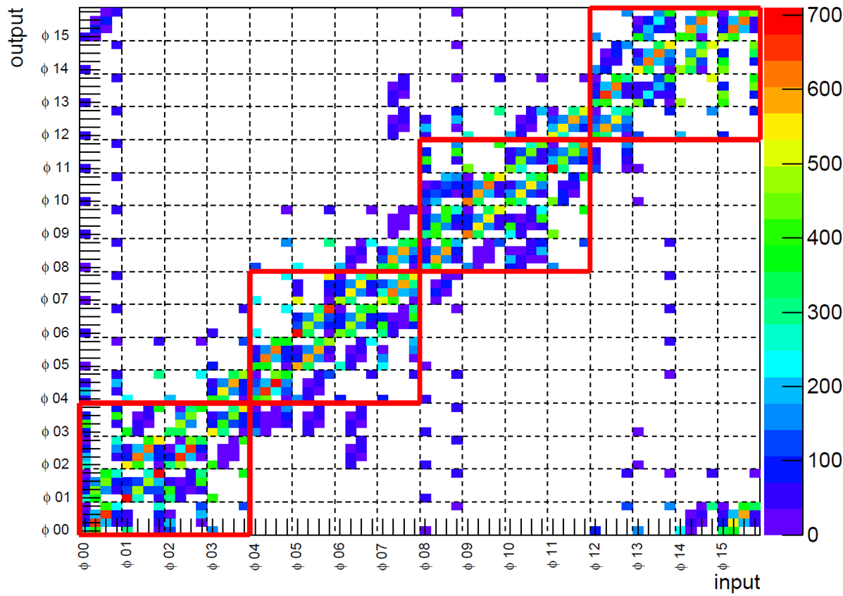
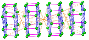
The ATLAS FTK is organized as a set of parallel processor units within an array of 64 eta-phi trigger towers. The matrix in Figure 1 shows the required data sharing in the data formatting stage first among the ATLAS FTK eta-phi trigger towers. Because the existing silicon tracker and front end electronics were not designed for triggering, the data sharing among trigger towers is quite complex, as shown in the matrix. The Data Formatter hardware design is dominated by the input and output requirements, and we analyzed the data sharing in early design stage using real beam data with the actual readout cable mapping. The four red boxes in the matrix represent crate boundaries. Boards within each crate communicate over the backplane. Fiber links are used when boards must communicate across crate boundaries. Our analysis shows that the data sharing between trigger towers is highly dependent upon upstream cabling and detector geometry. The ideal Data Formatter hardware platform should be flexible enough to accommodate future expansion and allow for changes in input cabling and module assignments. One example of such a system is shown in Figure 2, where each trigger tower is represented by a green ball and lines represent data paths.
III Design Concept
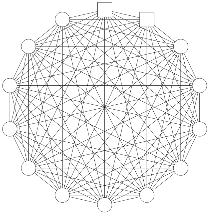
Our hardware design process followed a bottom up approach whereby we studied various track trigger architectures. Implementations involving full custom backplanes and discrete cables were considered. Eventually the full mesh Advanced Telecommunication Computing Architecture (ATCA) [3] backplane was found to be a natural fit for the Data Formatter requirements. The Fabric Interface of the full mesh backplane enables high speed point-to-point communication between every slot (Figure 3), with no switching or blocking. Each line in this diagram represents a channel which consists of up to four bidirectional lanes, which runs at the maximum speed of 40 Gb/s. Field Programmable Gate Array (FPGA) devices, which are abundant in local cells, memory, and high speed serial transceivers, were selected for the core processing element on each Data Formatter board.
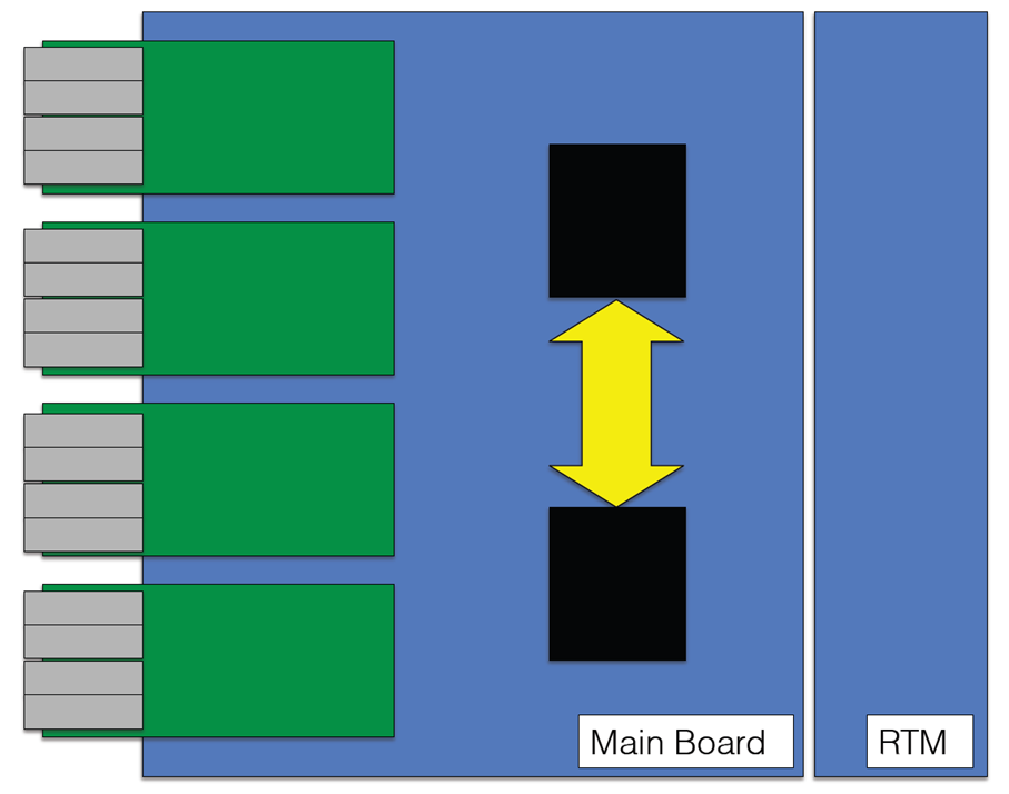
High speed serializer components in the FPGA are directly connected to the full mesh backplane fabric interface channels and also to pluggable fiber transceivers located on a rear transition module (RTM). Our first prototype ATCA board incorporated a pair of FPGAs, and thus required a high speed local bus to implement the three types of interconnects described in Figure 4.
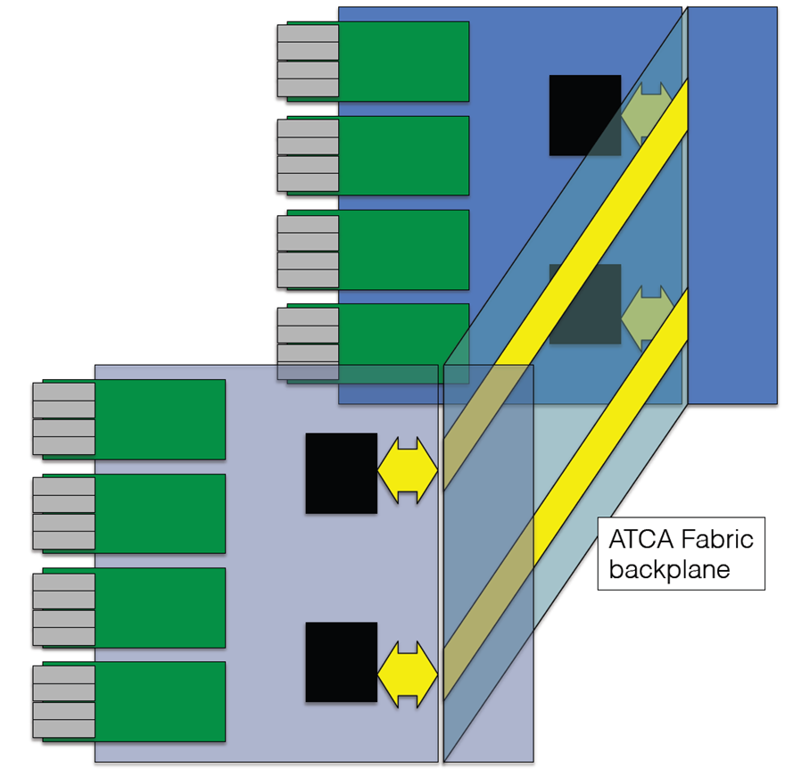

The full mesh backplane, when coupled with large FPGAs rich in high speed serial transceivers, offers a level flexibility previously unattainable in a conventional shared bus architecture. In effect, the system blurs the distinction between individual FPGAs and dramatically increases the processing power and I/O capability.
IV The Pulsar IIa Prototype
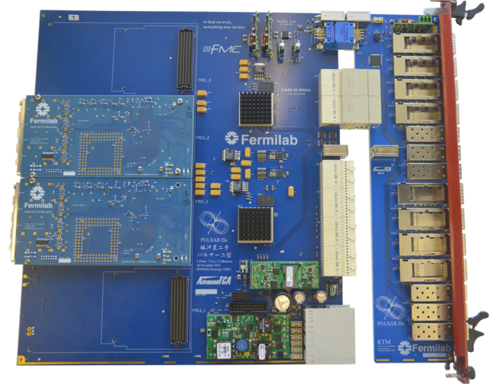
We designed the first prototype, the Pulsar IIa, to gain experience using the latest FPGAs with their high speed transceivers in an ATCA form factor. The Pulsar IIa consists of a front board and rear transition module (RTM) as shown in Figure 5. In addition we developed an FMC [4] mezzanine card which includes a smaller FPGA, four fiber transceivers, and a socket used for ASIC testing. A mini-backplane was also developed to facilitate standalone board testing on the bench top. This section describes the design details of each component. Further design details also can be accessed on our open web site [5].
IV-A Pulsar IIa Front Board
The Pulsar IIa front board is designed around a pair of Xilinx Kintex XC7K325T FPGAs. The block diagram of the board is shown in Figure 6. Each FPGA has 16 high speed serial transceivers (GTX) which support data rates up to 10 Gb/s. Of these 16 GTX transceivers 9 connect to the fabric interface, 6 connect to the RTM, and the last GTX transceiver is used for the local bus.
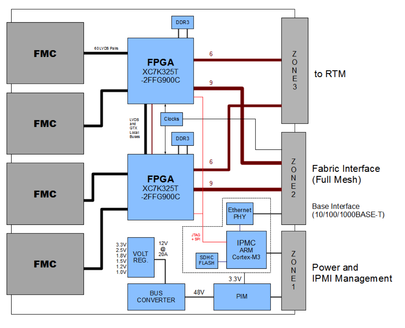
Each board supports up to four high pin count FMC mezzanine cards, which are connected to the main FPGAs using general purpose LVDS signal pairs. The FMC form factor has in recent years become a popular choice with Xilinx development boards and many third party developers. When the Pulsar IIa board is used as the FTK Data Formatter four cluster finder input mezzanine cards will be used.
A Cortex-M3 microcontroller is used as an Intelligent Platform Management Controller (IPMC), which is required on all ATCA boards. This microcontroller is responsible for the following:
-
•
Implementing the IPMI protocol and communicating with the ATCA shelf manager board(s), coordinating hot swap operations, etc.
-
•
Running Telnet and FTP servers which are accessed via the 100BASE-T Base Interface Ethernet port.
-
•
Managing firmware images on a micro SDHC flash card.
-
•
Programming the FPGAs via JTAG and monitoring over an SPI bus.
-
•
Reading various board temperature and voltage sensors.
-
•
Communicating with the RTM over an I2C bus.
IV-B Rear Transition Module
The Pulsar IIa RTM conforms to the PICMG3.8 standard [6] and is considered an intelligent-FRU device. A small ARM microcontroller on the RTM continuously monitors the status of the 8 QSFP+ and 6 SFP+ pluggable transceivers. The microcontroller also communicates with the front board IPMC microcontroller and coordinates hot swap sequencing. Each of the Pulsar IIa FPGAs connects to one QSFP+ transceiver and two SFP+ transceivers on the RTM.
IV-C Mezzanine Card
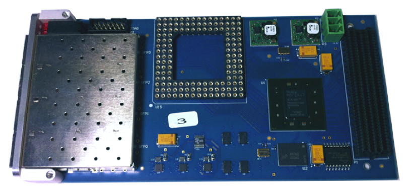
The Pulsar IIa supports up to four FMC mezzanine cards with the high pin count (HPC) LVDS interface. Mezzanine cards may contain FPGAs, pattern recognition ASICs, fiber optic transceivers, or any other custom hardware. We developed our FMC test mezzanine card, shown in Figure 7, in order to become familiar with the FMC form factor and to study high speed LVDS communication between FPGAs. The test mezzanine card features a Xilinx Kintex XC7K160T FPGA, 4 SFP+ transceivers, 128MB DDR3, and a 144 pin socket used for testing custom ASIC chips, primarily aimed at testing pattern recognition associative memory devices [7]. The FMC connector supports 3.3V and 12V power. An I2C bus and JTAG interface are also provided for slow controls and in-system programming.
IV-D Mini Backplane
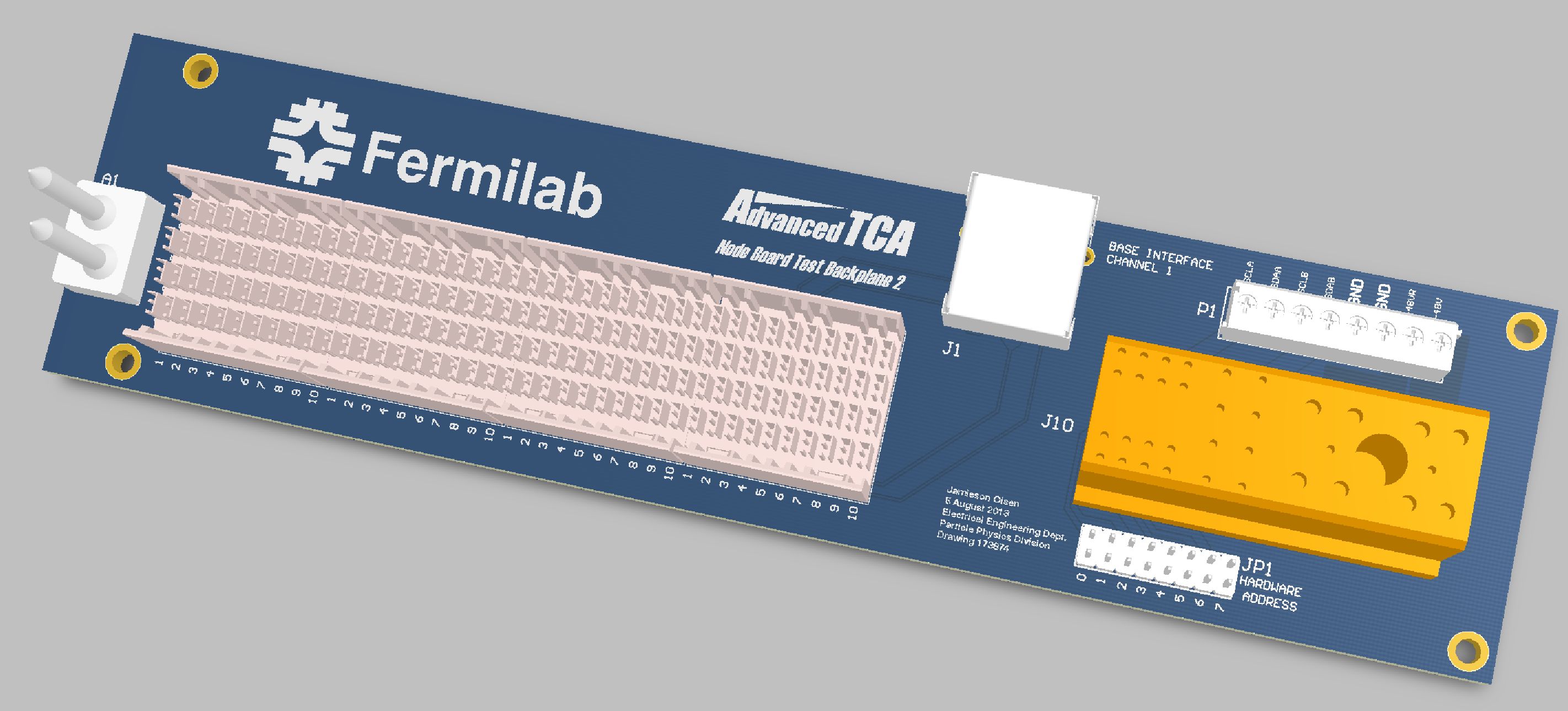
The Mini Backplane (Figure 8) was developed to support stand alone testing of a single Pulsar IIa board and RTM on the bench top. Power is supplied from a 48VDC bench supply. The Base Interface Ethernet port is brought out to an RJ45 connector which may then be connected to a PC and used for communicating with the IPMC microcontroller.
The Mini Backplane also loops back each Fabric Interface port. This loopback feature has proved to be very useful in testing and characterizing the performance of the GTX serial transceivers outside of the crate.
V Test Results
V-A Board-level testing
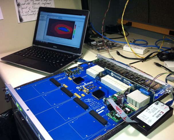
Figure 9 shows our bench top test setup, which is used to check basic functionality such power supply operation, IPMC microcontroller communication, FPGA programming and GTX loopback tests.
The FPGA GTX transceivers are driving data in the test-stand system in the Fabric Interface channels, the RTM channels and the Local Bus. It turns out that the FPGAs achieved a bit error rates (BER) less than level in long-running loop back tests. The upper limit of BER is defined to be if there is no single error detected during the test. Table I summarized the measured upper limit.
| Speed | BER upper limit | |
|---|---|---|
| Fabric Interface channels | 6.25 Gb/s | |
| RTM channels | 6.25 Gb/s | |
| Local Bus | 10 Gb/s |
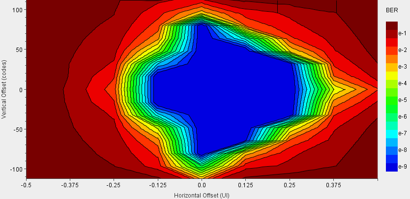
In addition to the BER test, we performed a receiver margin analysis, or eye scan, using the Xilinx IBERT tool. The Kintex-7 GTX transceivers have built-in diagnostic features which provide a mechanism to measure and visualize the receiver eye margin after RX equalizer [8]. Sweeping the receiver sampling point and vertical offset voltage enables the generation of a BER map or statistical eye diagram, where the color represents . Figure 10 shows an example of the measured statistical eye diagram and the open blue region indicates that we can have error free operating points. The size of eye corresponds to the quality of the high speed serial communication after the RX equalization. All GTX transceiver channels have been tested and characterized using the IBERT tool. Furthermore, the eye scan has been done with a Xilinx Kintex-7 evaluation kit (KC705) [9], which provides a ”golden” reference for comparison studies. Comparing the Pulsar IIa eye diagrams against the Xilinx reference design helps us learn more about high speed layout techniques, which will be used in the next iteration of the board (Section VI).
Communication over the LVDS lines between the FMC mezzanine and the main FPGAs has been tested successfully at 400 MHz single data rate (SDR) and 200 MHz double data rate (DDR). Thirty-four LVDS pairs running at this speed yield a bandwidth of 13.6 Gb/s, which exceeds the ATLAS FTK requirements for the Data Formatter board.
V-B Crate-Level Testing
A crate-level testing followed the single board-level testing. We set up an ATCA shelf with a network switch blade in the hub slot and seven Pulsar IIa front boards as well as RTMs in the node slots, as shown in Figure 11.
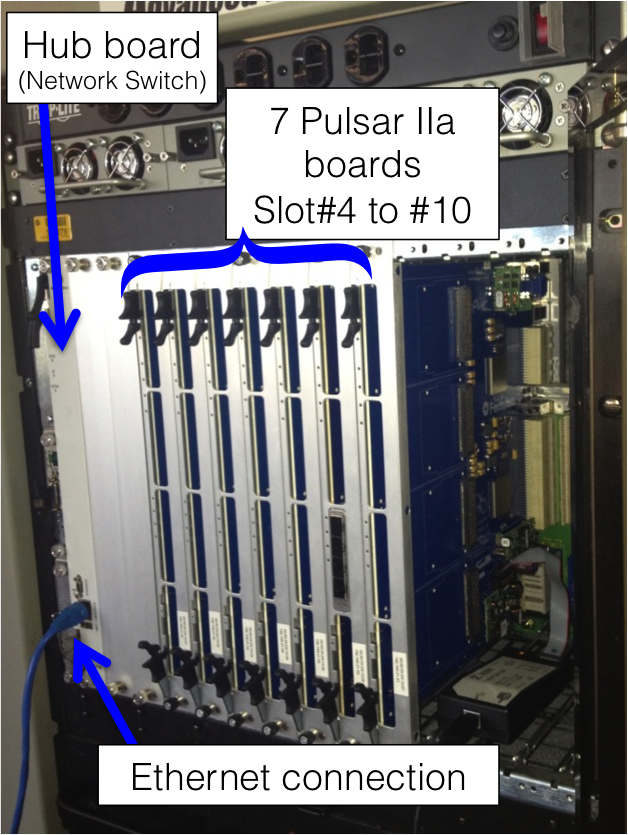
In our system test the IPMC microcontroller communicates with the switch blade over the Base Interface network. We first log into the switch and then telnet into each Pulsar IIa board, where commands are issued to program the FPGAs and monitor various board sensors. The default firmware image is setup to drive data over all GTX transceivers to the fabric, RTM and local bus channels.
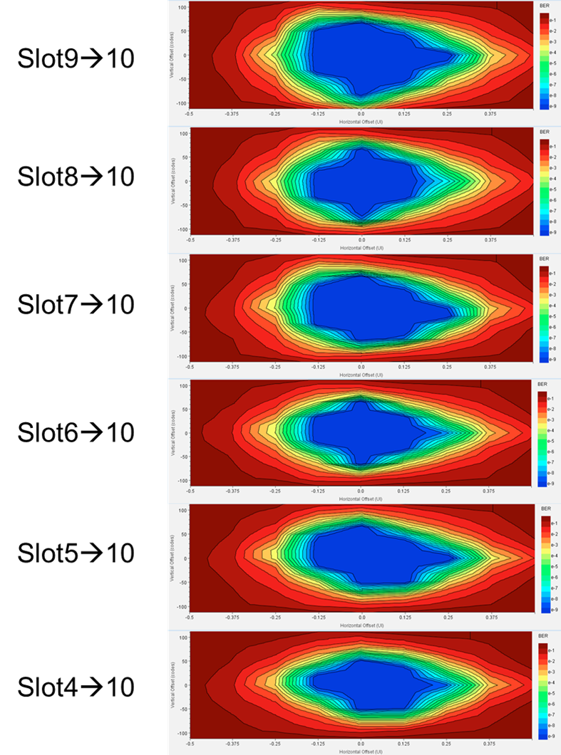
The Xilinx IBERT tool has also been used in the the crate to test the backplane performance. While our 10G ATCA backplane is rated for only 3 Gb/s per lane it has proven to work admirably at up to 6.25 Gb/s across all slots, as shown in Figure 12.
VI Pulsar IIb
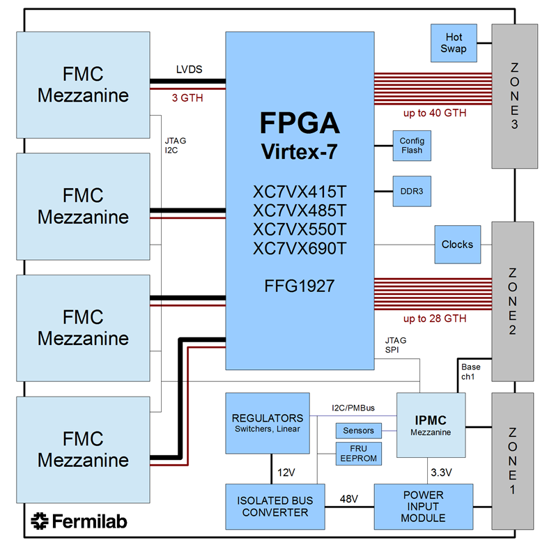
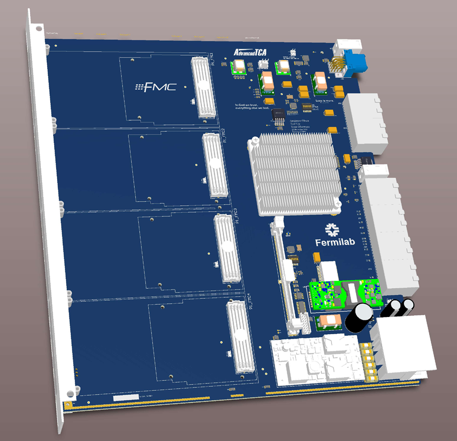
Leveraging the experience we gained through designing, building and testing the Pulsar IIa system we are in the final stages of laying out the next generation board, the Pulsar IIb (Figure 13 and Figure 14). The new board design replaces the two Kintex K325T devices with a single large Virtex-7 FPGA. The GTX transceiver count has increased up to 80 channels, providing a significant bandwidth increase to the RTM, Fabric and Mezzanine cards. The power regulator sections of the board have been redesigned to handle the increased power required by the Virtex-7 FPGA.
The Pulsar IIb boards will be used for the ATLAS FTK Data Formatter system. We anticipate that the boards will also be used for CMS L1 tracking trigger early technical demonstrations [10].
VII Conclusion
The Pulsar IIa is our first ATCA prototype board and works as designed, as demonstrated by our successful stand-alone and crate-level tests. Through this prototype development process we have gained experience using the latest Xilinx FPGAs and high speed serializers to communicate over the ATCA full mesh backplane. Furthermore, the Pulsar IIa boards have successfully interfaced with other ATCA system components such as commercial switch blades and shelf manager cards.
The Pulsar IIb boards will be used in the ATLAS FTK Data Formatter system starting in 2015. The Pulsar IIb design forms the basic building block of a high performance scalable architecture, which may find applications beyond tracking triggers, and may serve as a starting point for future Level-1 silicon-based tracking trigger R&D for CMS, where the full mesh backplane is used most effectively for sophisticated time multiplexing data transfer schemes.
Our baseline design also works well as a general purpose FPGA-based processor board. The design may prove useful in scalable systems where highly flexible, non-blocking, high bandwidth board to board communication is required.
References
- [1] The ATLAS Collaboration, Fast TracKer (FTK) Technical Design Report, CERN-LHCC-2013-007, ATLAS-TDR-021-2013, 2013
- [2] Jamieson Olsen, Tiehui Ted Liu, Yasuyuki Okumura, Data Formatter Design Specification, FERMILAB-TM-2553-E-PPD, 2013
- [3] PICMG 3.0 AdvancedTCA Base Specification (Shortform), http://www.picmg.org/v2internal/shortformspecs.htm
- [4] FPGA Mezzanine Card Specification (VITA57.1), http://www.vita.com/fmc.html
- [5] ATCA at Fermilab webpage, http://www-ppd.fnal.gov/EEDOffice-w/Projects/ATCA/
- [6] PICMG 3.8 AdvancedTCA Rear Transition Module Zone 3A Specification, http://www.picmg.org
- [7] Ted Liu et al., A New Concept of Vertically Integrated Pattern Recognition Associative Memory, Fermilab-CONF-11-709-E, 2011. Published in Proceedings of the 2nd International Conference on Technology and Instrumentation in Particle Physics (TIPP 2011), Physics Procedia,Volume 37, 2012, Pages 1973 - 1982
- [8] 7 Series FPGAs GTX/GTH Transceivers User Guide, 2013
- [9] Xilinx Kintex KC705 Development Board http://www.xilinx.com/products/boards-and-kits/EK-K7-KC705-G.htm
- [10] J. Olsen, T. Liu, Y. Okumura, A Full Mesh ATCA-based General Purpose Data Processing Board : Pulsar II, FERMILAB-CONF-13-526-CMS-PPD, to be published in Proceedings of Topical Workshop on Electronics for Particle Physics 2013 (TWEPP-13 ) in the Journal of Instrumentation (JINST) Proceedings Section