Development of a plasma panel radiation detector
Abstract
This article reports on the development and experimental results of commercial plasma display panels adapted for their potential use as micropattern gas radiation detectors. The plasma panel sensor (PPS) design and materials include glass substrates, metal electrodes and inert gas mixtures which provide a physically robust, hermetically-sealed device. Plasma display panels used as detectors were tested with cosmic ray muons, beta rays and gamma rays, protons, and thermal neutrons. The results demonstrated rise times and time resolution of a few nanoseconds, as well as sub-millimeter spatial resolution compatible with the pixel pitch.
1 Introduction
This article reports on the development and testing of commercial plasma display panels adapted for use as a novel type of micropattern gas radiation detector. Plasma display panels (PDP) are commonly used in televisions and graphical display devices. Their design and production is supported by an extensive and experienced industrial base with four decades of development. The application of PDPs as particle detectors is referred to as a plasma panel sensor (PPS) [1, 2, 3, 4, 5, 6]. The primary motivation underlying the PPS concept is to use well established manufacturing processes of PDPs to develop scalable, inexpensive and hermetically sealed gaseous detectors with the potential for a broad range of commercial and research applications.
A commercial PDP consists of millions of cells per square meter, each of which can initiate and sustain a plasma discharge when addressed by a bias-voltage signal [7]. A PDP, in the simplest matrix configuration, consists of an envelope of two flat, parallel, glass plates with line electrodes deposited on the internal surfaces. The plates are sealed together at the edges with the top and bottom electrodes aligned perpendicularly. The gap separating the two plates is between 200-400 m and is filled with a Penning gas mixture of mostly Xe, Ar or Ne, typically at pressures of about one-half atmosphere. In such a structure, a pixel is made of an electrode intersection and gas gap.
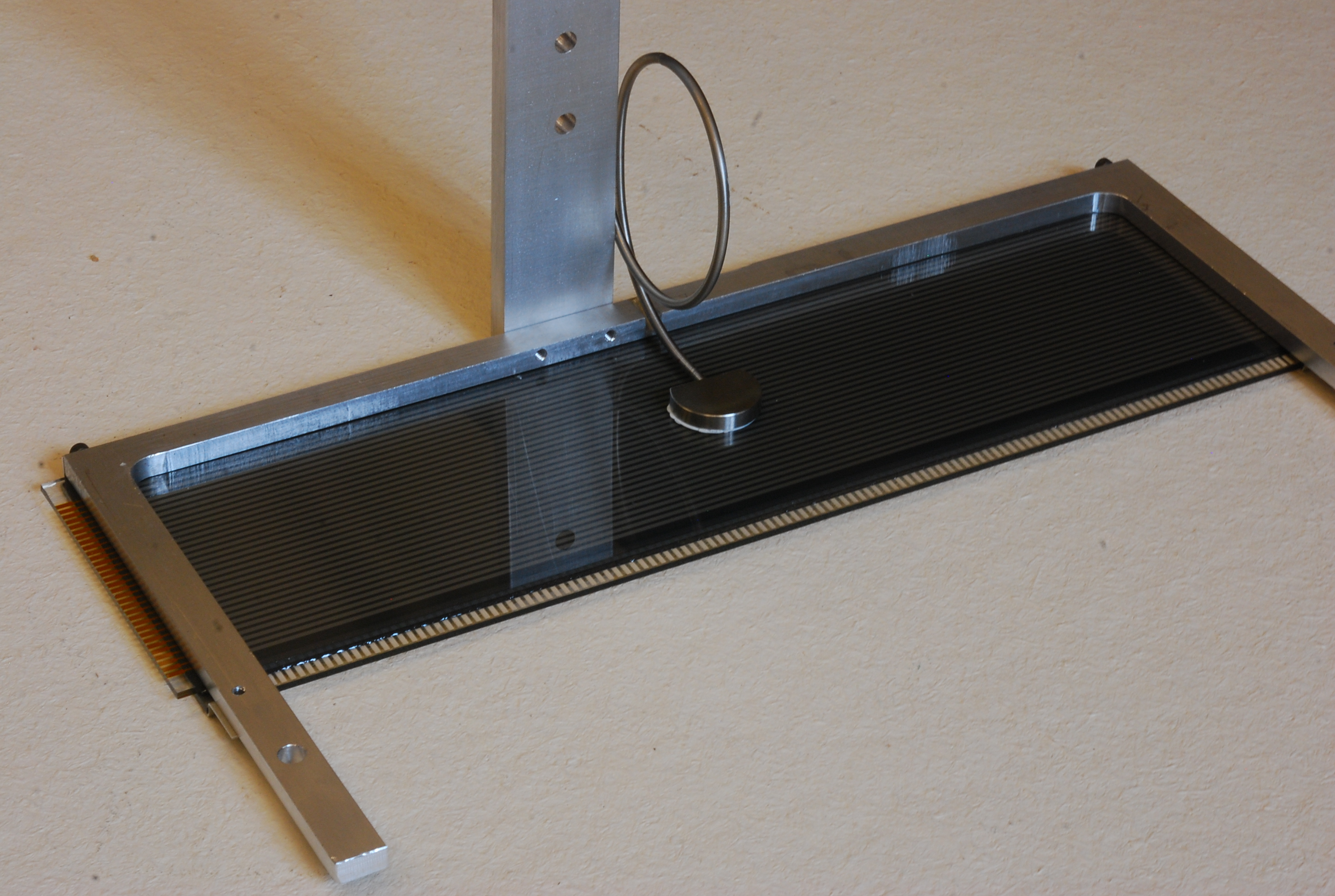
A PPS incorporates the general structure of a PDP, but instead of actively inducing a plasma discharge with an applied voltage delivered to an addressed pixel, the plasma discharge is caused by ionizing radiation entering a PPS cell biased with a constant DC voltage above the Paschen potential. Results reported in this article were produced with commercial PDPs modified in specific ways to allow them to be used as particle detectors. They operated with DC bias voltages, had no dielectric barriers to isolate individual cells and had no phosphors in the cells. These panels were a simple matrix of anodes and cathodes with a gas filled gap of a few hundred micrometers. An example of a test device is shown in Figure 1. The modifications made to the panels were:
-
1.
Panels were normally fabricated with a hermetically sealed glass port. This was replaced with a stainless steel valve assembly that connects the panel to a gas mixing and vacuum pump system.
-
2.
The original Ne based panel gas was replaced with a test gas.
-
3.
The electrodes in the commercial panels were made from both Ni and SnO2:F. A selection of the tested PPS panels used all Ni electrodes. The Ni was found to be much more resistant than the SnO2:F to sputtering degradation.
-
4.
The electronics required for panel display operation was replaced with signal extraction circuitry on the readout anode electrodes.
-
5.
The high voltage bias was routed through quench resistors connected to each cathode electrode.
The above modifications allowed these commercial units to serve as a useful test bench for the PPS concept. The modified commercial panels served as prototypes for investigations and the results obtained from them have informed the next generation of PPS panels, the subject of a future paper. Commercial PDPs are sealed devices designed to work for hours. One panel filled with a Xe-based gas mixture at 600 Torr and hermetically sealed in 2003 produced signals when operated as a PPS seven years later, clearly demonstrating the long term stability of the materials and gas mixture.
The panels evaluated in this report differed from each other in the electrode material, pixel density and size, and gas gap, that is separation of the anodes and cathodes. For the hit position studies, a type MP plasma panel was employed with a pixel pitch/granularity of mm. For the investigation of panel timing, efficiency and response to various particle types a larger VPA panel was used with a pixel pitch/granularity of mm. The specifications of these two different types of panels are summarized in Table 1.
| Panel type VPA | Panel type MP | |
| HV electrodes material | Ni | Ni |
| HV electrodes width (mm) | 1.40 | 0.44 |
| HV electrodes length(mm) | 81 | 65 |
| RO electrodes material | Ni | SnO2:F |
| RO electrodes width (mm) | 1.27 | 0.71 |
| RO electrodes length(mm) | 325 | 131 |
| Electrodes pitch (mm) | 2.54 | 1.02 |
| Active pixel area (mm2) | 1.50 | 0.22 |
| Packing fraction | 23.5% | 22.0% |
| Gas gap (mm) | 0.38 | 0.29 |
| Glass thickness (mm) | 2.23 | 2.23 |
| Electrodes thickness (mm) | 0.02 | 0.02 |
| Dielectric mesh thickness (mm) | 0.02 | 0.02 |
| VISHAY product number | PD-‐128G032-‐1 | PD-‐128G064-‐1 |
Signals were investigated from panels filled with different gas mixtures at various pressures, exposed to radiation from radioisotope sources, particle beams and cosmic rays. The various mixtures were either commercially obtained or produced in our gas mixing system.
2 Operational principles
The use of PDPs as particle detectors requires that a charged particle will generate enough ion-pairs to initiate an avalanche leading to a discharge. This operational mode must be beyond the proportional region in the Geiger region [8] of gas ionization to achieve the desired fast, high gain response. This mode of operation of a cell can yield copious photons, photoelectrons and metastable atoms which could, due to the lack of physical barrier between the pixels, propagate and spread the discharge to other pixels.
Various mechanisms mitigate discharge regeneration in a PPS. Small amounts of gases such as CO2 or CF4 are added to the primary gas to absorb the photons through non-radiative vibrational and rotational excitations. Penning type mixtures [9] may also be used wherein the dopant gas has a first ionization energy level lower than the host gas excited states, e.g., CO2 or CF4 in Ar. The Penning transfer process allows for collisional de-excitation of the long-lived, metastable states. Finally, the discharge is externally quenched with a large resistor connected in series to each pixel or chain of pixels on the high voltage (HV) electrode. The pixels are then allowed to recover on a time scale determined by the time constant, where C is the effective pixel capacitance, effectively dominated by the choice of the quench resistor. This time constant should be commensurate with the time required for positive ions to neutralize and gas metastable species to decay [10].
The detailed mechanism for the discharge process is uncertain. A classic Townsend gas avalanche is limited by space charge buildup that negates the applied electric field, known as the Raether limit [11, 12]. The gas discharges that occurred in PPS pixels produced charge in excess of the Raether limit. This is shown in the next section where the signal is described by a simple capacitive discharge model. This model is valid after the discharge has fully evolved between the pixel electrodes. We do not yet have the complete description of the progression from avalanche to full discharge that is required to accurately predict the gas dependent signal evolution.
2.1 Signal model
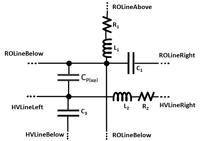
An idealized model for one pixel in the PPS detector is shown in the equivalent circuit model in Figure 2, where is the quench resistor (), is the pixel total effective capacitance and is the termination resistor over which the signal is read.

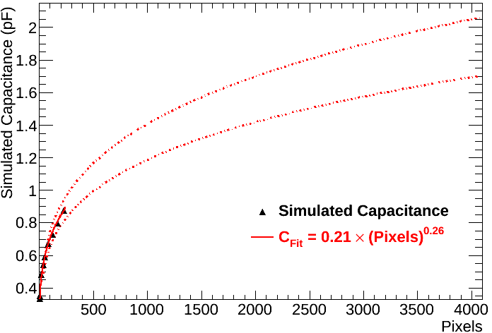
The effective pixel capacitance includes the capacitance presented by the crossing of two orthogonal electrode lines and that from stray or parasitic couplings with all the other electrodes in the panel. This effective pixel capacitance in a type VPA panel was modeled using the COMSOL [14] package which uses the finite element method to solve the Poisson equation. This three dimensional model simulates the entire volume of the detector and specifies the electrode dimensions, pitch, gap and number of electrodes in an orthogonal square array. The model did not account for the dielectric glass substrates, nor the thin dielectric mesh overlaid on the electrodes at the cell perimeter. The computation was run for a series of increasing array sizes up to at which point further increases became computationally impractical. The simulated capacitance versus number of pixels, shown in Figure 3, was fit and extrapolated to the VPA panel array size of pixels 128 pixels. The extrapolated result was pF, where the uncertainty was determined from the fit errors. By comparison, the effective capacitance was also measured with an Agilent 4263B LCR meter. A series of ten measurements were conducted for various pair combinations. The measured value was pF, consistent with the computation while the capacitance of a single electrode pair was calculated to be almost an order of magnitude lower, at 0.35 pF.
An estimate of the amount of charge in a signal with an amplitude of several volts is given by: where is the measured signal amplitude, is the pulse width and is the termination resistance. Average values for MP type panels (see Table 1) are volts and 5 ns, yielding , or about electrons. Alternatively, where is the change in the bias voltage on one pixel during discharge. is about 300 volts on top of a bias voltage of 1000 volts. is the effective capacitance of the pixel described above, yielding a similar estimate of the charge. This amount of charge greatly exceeds gain expected from the Raether limit [11, 12].
The signal characteristics were further described by a SPICE [16] model which simulated the electronic response of a single pixel embedded among neighbors, connected via direct and stray capacitances, inductances and line resistance. In this model the fundamental single pixel circuit included the capacitance of the cell, the self-inductance and resistivity of the lines, and the nearest neighbor parasitic coupling capacitances. Not included in the SPICE model were the readout electronics (printed circuit card, passive components, cables, etc). The input parameters were determined with a COMSOL-based electrostatic model. Figure 4 shows the schematic of the SPICE equivalent circuit model of one cell in the panel. The physical development of the signal in the pixel was not modeled. It was introduced as an impulse at capacitor .
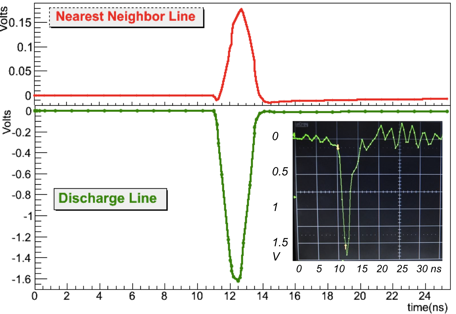
The full SPICE model connected all the neighboring cells to form a array of pixels. Larger array sizes are computationally expensive and produce the same results. Figure 5 shows the signal produced by the central pixel in the array and also a smaller transient pulse induced in an adjacent neighboring electrode. The important qualitative attributes of the SPICE modeling included the pulse shape and the transient pulses on other lines. The signal induced in neighboring pixels had greatly reduced amplitude and the opposite polarity of the discharging cell.
2.2 Pixel dead time
During the discharge, electric current starts to flow between the pixel electrodes. This current results in voltage dropping on the quench resistor, reducing the electric field between the pixel’s electrodes. In these conditions the pixel discharge is not sustained; the discharge terminates and the gas neutralizes. The time required for the pixel electric field to regain a strength sufficient to enable a new discharge is determined by an RC time constant, where R is the quench resistance and C is the effective pixel capacitance. For a quench resistance of 100 M and approximately 2 pF effective capacitance, the RC time is seconds. The pixel dead time was experimentally determined to be about three times this RC time constant. For the modified commercial PDPs reported here, the quench resistance was applied to an entire chain of 24 pixels serviced by one HV line, rather than a single isolated pixel.
The RC time constants, and thus the pixel dead time, should be optimized according to the following considerations:
-
1.
If the dead time is not sufficiently long and the positive ion cloud and/or the gas metastable states are not neutralized then the discharge can restart without an external trigger, giving rise to more than one pulse per incident particle.
-
2.
For gas recovery dead time longer than necessary, the observed signal rate would saturate at an unnecessarily low rate and the panel will lose efficiency at high irradiation rates.
The optimal dead time changes with the gas content, with values in the range between 0.1 ms to a few milliseconds per pixel.
3 Data Acquisition
The characteristics of the pulses induced in the panel were measured with a 1 gigasamples/sec (GSPS) digital oscilloscope or an evaluation board of the DRS4 chip [17]. The evaluation board was equivalent to a four channel, 5 GSPS digital oscilloscope with control, readout and data storage performed by an external computer.
Extraction of the signals from the prototype PPS panels was done with a custom designed PCB readout card connected to the panel electrode pads. The signal was picked off of a termination resistance ( in Figure 2). These readout cards included attenuators for each readout line since the observed several volt signal amplitudes were too large for the readout electronics.
In order to instrument more readout lines and thus have a larger active area in the panel, a more elaborate DAQ system was used. For this purpose a portable version of the readout system for the ATLAS precision muon chambers called MiniDAQ [18] was adopted. This implementation of the MiniDAQ system was capable of recording integrated pulse height and time relative to the trigger for up to 432 channels with a sub-nanosecond (0.78125 ns) least significant bit.
For position measurement scans, where only basic hit information was needed, either a Wiener NIMbox [19] module, configured as a 20 channel scaler, or a CAEN V560 16 channel scaler [20] was employed to acquire data. In these measurements, signal processing was done in three stages. The panel signals were first discriminated. One set of discriminator output logic signals were injected into the scalers. A second set of discriminator signals were logically OR’ed, and used to generate a 1 s long veto which was returned to the discriminators with a measured delay of 60 ns. This veto blocked counts in the scaler from the occurrence of later pulses that might occur in a panel.
For each of the above dedicated data acquisition methods, analysis software was written using LabVIEW [21] and C++/ROOT [22].
3.1 Radioactive sources
Because of the low rate of cosmic ray muons through the instrumented area of the panels, a number of measurements reported here were made by using radioactive emitters: 90Sr and 106Ru. These measurements probed the panel sensitivity to the applied voltage by measuring hit rates, and gauged the position resolution. The 90Sr source (3.7 mCi), produces, at the end of its decay chain a spectrum with a maximum energy of 2.28 MeV [23]. A 106Ru source, about Ci at the time of the experiments here reported, yields a energy spectrum end point of 3.54 MeV [24]. The sources were separated from the active pixel volume by various air gaps and the 2.23 mm glass plate of the PPS, resulting in substantial beta energy loss. Measurements with radioisotopes were self-triggered by the logical OR of all the readout channels after discrimination.
4 Measurements
The measurement results reported here included evaluation of the response of type VPA and MP panels (see Table 1) filled with various gas mixtures using Ar, CO2, CF4 and, for thermal neutron detection, 3He. The panel response to radiation, background hit rates and the occurrence of discharge spreading were investigated using low energy particles, rays, thermalized neutrons from radioactive sources and cosmic ray muons. Efficiency and time response for a few gas mixtures and pressures were probed using cosmic ray muons. Position reconstruction and spatial resolution were explored using a slit-collimated radioactive source whose position was set with a computer-controlled servo-motor arm.
4.1 Response to sources
All panel types responded to the radiation emitted from 90Sr and 106Ru sources, with all of the tested gases. Panels were tested at pressures ranging from as low as 200 Torr to slightly below atmospheric pressure, because the tested PDPs were not designed for positive pressure. This paper reports measurements made at pressures from 600-730 Torr. Figure 6 shows a representative signal induced by a 90Sr source irradiating an MP type panel. Similar signals were observed using sources in a panel filled with Xe at 600 Torr [4], sealed seven years before the observation [1].
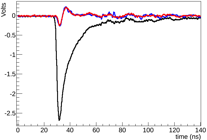
The signals from all the tested gases were characterized by large amplitudes of 1-10 V volts that depended highly on the gas content and panel type, as well as fast rise times, around 1 to 3 ns. These general features were also evident in the SPICE signal simulation shown in Figure 5. The large signals did not require amplification and sometimes required attenuation. For each test configuration of panel type, gas mixture, pressure and high voltage, the induced signal amplitudes were uniform, with approximately 2% variation. This can be seen in one case in Figure 7 and is expected for a Geiger type discharge.
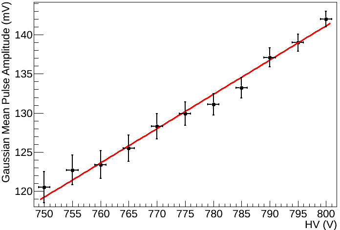
Two experiments were conducted to validate the COMSOL and SPICE models. In the first, a type MP panel (see Table 1) filled with a gas mixture of 10% CF4 in Ar at 600 Torr was used. The dependence of the signal amplitude on the applied voltage was measured, the operating voltage range was chosen for maximum signal rate with minimum source-free (background) rate. This was expected to be linear, based on the idealized capacitive discharge model expressed by the circuit in Figure 2. The waveform of a single pixel pulse at increasing HV was recorded. The signal amplitude was then fitted with a Gaussian function. Figure 8 displays the dependence of the means on the applied HV, confirming the expected linear relationship.
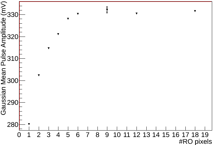
In a second experiment, a type VPA panel (see Table 1) filled with a gas mixture of 10% CF4 in Ar at 600 Torr was used at fixed operating voltage of 1100V. The signal amplitude dependence on the number of readout lines instrumented was measured. During these measurements, unconnected electrodes were left floating. The exponential behavior of the data in Figure 9 shows that with five or more lines the amplitude of the signal reached an asymptotic value, consistent with the use of a matrix for the SPICE electrical simulations.
4.1.1 Voltage scan
The PPS response to radioactive sources and the associated background (i.e. no source) were measured over a range of applied HV. Figure 10 presents an example of a voltage scan taken with a gas content of 1% CF4 in Ar at 600 Torr. In this measurement one HV line was quenched with a 44 M resistor and four readout channels were instrumented. For every applied voltage two measurements were taken, one in which a 106Ru source was positioned in a fixed location above the panel’s active area, and one with the source removed.
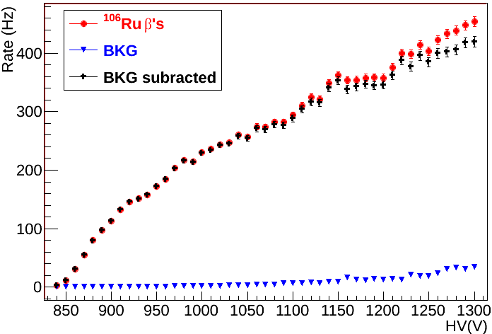
These measurements provided a relative rate dependence on the HV. The net rate appeared to reach a plateau at about 1150 V, extending for about 60 volts. The dead time is around 350 s, so in this region the maximum fraction of hits potentially lost because of the dead time is below 12%. Importantly, the source-free rate remained very low for a large range of HV before gradually increasing at higher values of the applied HV. The source-free hit rate was primarly attributed to discharges resulting from spontaneous formation of ion pairs in the gas, from electron surface emission due to stochastic collisions and from photoelectric processes. At higher applied HV the probability for spontaneous ionization and regeneration increased leading to a higher background hit rate.
4.1.2 Quench resistor dependence
For a given panel and gas mixture, a characteristic response curve was generated, giving the dependence of the source induced hit rate on the HV quench resistance. This is shown in Figure 11, plotted as a function of the reciprocal of the line quench resistor. For this measurement the panel was filled with 1% CO2 in Ar at 600 Torr and was operated at 815V. The radioactive source was 106Ru and the hits were collected from four readout electrodes crossing a single HV line. The quench resistors cover the range from 10-600 M.
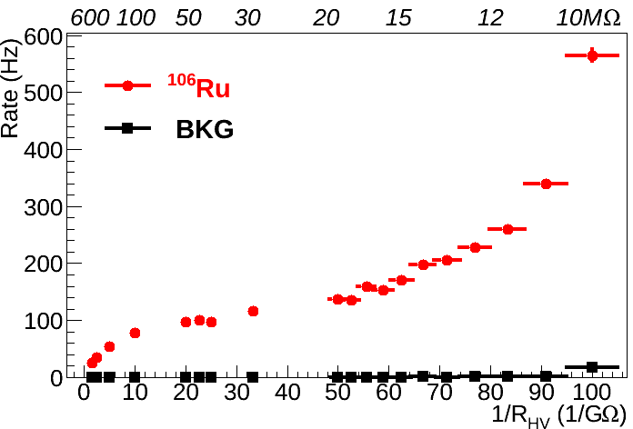
This measurement showed that for resistance values below 20 M the recovery time was insufficiently long to prevent the formation of afterpulses. These afterpulses increased the measured hit rate. Conversely, for resistance values above about 100 M the pixel’s RC constant was too high for the applied source intensity. This was because the time between successive hits from the source was less than the pixel recovery time, so that the observed hit rate saturated, being limited by the RC constant. For this specific gas mixture, pressure and source intensity, the working range of quench resistances was obtained where the measured hit rate was flat.
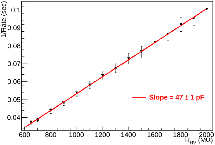
These measurements were extended to very high quench resistor values, shown in Figure 12, using exactly the same setup parameters as in Figure 11. This measurement probed the recovery time constant where is the number of RC time constants needed for a cell’s recovery, is the quench resistance, is the pixel’s effective capacitance (described earlier) and is the number of instrumented pixels. The slope of the linear fit to the data was pF. Using the measured value for the capacitance, pF and , then . This result suggested that, for the cell to become fully active after a discharge, the electric field must have returned to within a few percent of its pre-discharge strength. For a 44 M external quench resistance, as used for the experiment in Figure 10, the recovery time for a single HV line is around 500 s.
4.2 Measurements with cosmic ray muons
Cosmic muons were used to explore the PPS response to minimum ionizing particles (MIPs). The main features investigated were the efficiency and timing response. Uniformity was also measured. For these measurements an external plastic scintillator trigger was used. This trigger provided the necessary coincidence and timing of signals induced in the panel to cosmic muons.
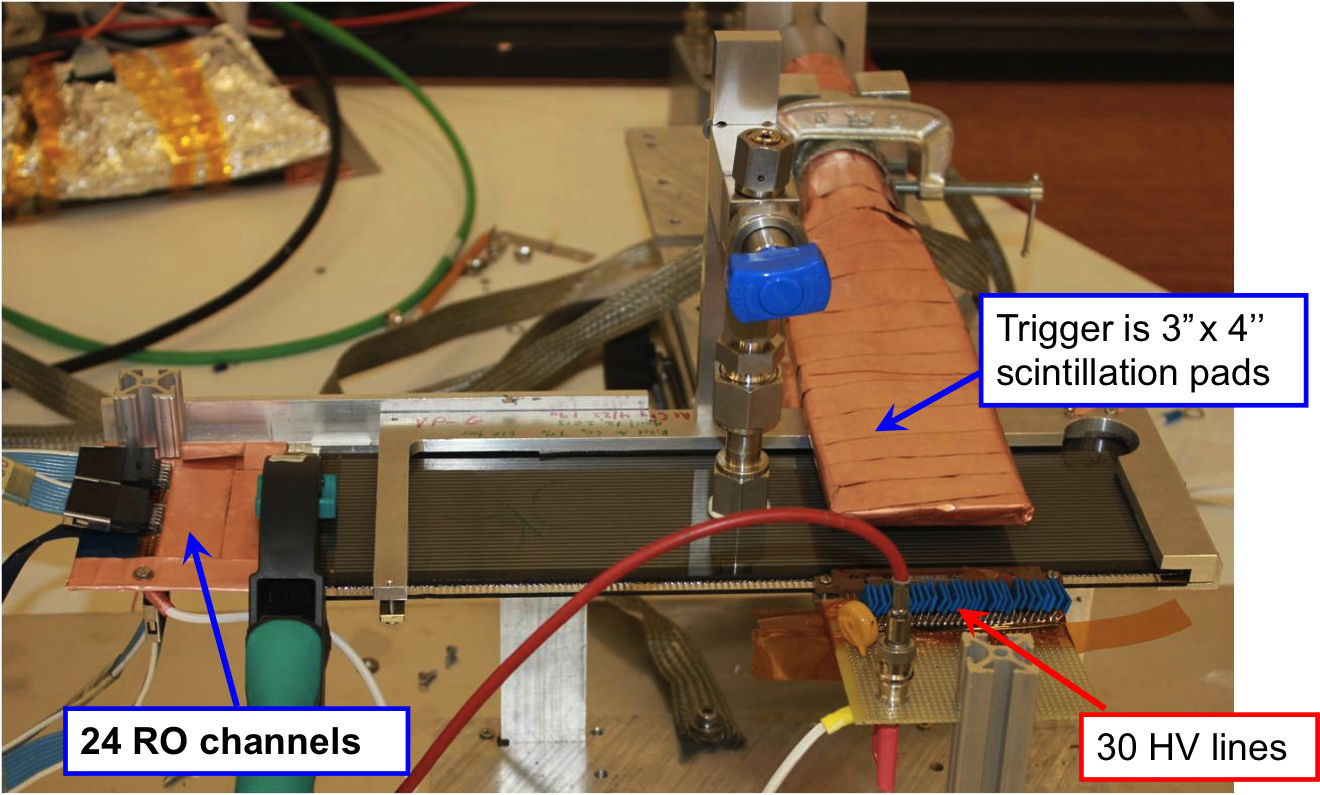
The trigger hardware was formed by two scintillator paddles (7.5 cm 10 cm) placed above and below the instrumented areas of the panel (see Figure 13).
The trigger signal was the time coincidence of the discriminated pulses (20 ns wide, NIM logic signals) from the two scintillator photomultipliers. The coincidence window of the panel and trigger was 2 s. The uncorrelated single count hit rate in each scintillator was tens of Hz, so the rate of accidental coincidences was negligible.
4.2.1 Uniformity of response
Commercial PDPs are fabricated with tolerances not necessarily as stringent as required for detectors. As more HV and readout lines were instrumented, variations in the count rates were observed on different parts of the panels. A study was performed to obtain a baseline measurement of the uniformity of the panel as a function of position.
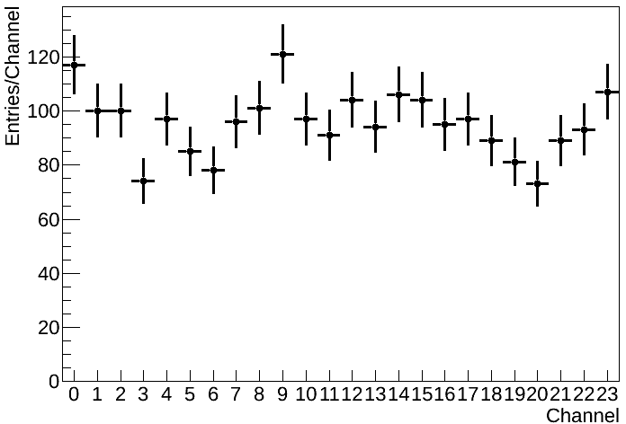
Figure 14 shows the distribution of cosmic ray muon PPS hits per readout line summed over the 30 HV lines instrumented. For this panel, the RMS fluctuation around the mean of 95.4 is less than 12%. This variation, however, reflects the convolution of the panel non-uniformity with the trigger spatial non-uniformity, evaluated to be no more than 10% across the instrumented area of the panel. These variations are expected based on the non-uniformities of the thick film electrode printing technique used in PDP construction.
4.2.2 Secondary pulses
Secondary pulses, referred to here as secondaries, are defined as those pulses occurring after the primary one either on the same pixel (afterpulses) or in a different location as the result of discharge spreading. Discharge spreading is primarily caused by both drifting metastable species and by VUV photons propagating to nearby pixels. The results of the position scans (see Section 4.3) suggested that detrimental effects of secondaries are limited.
The frequency of secondaries is dependent on the panel geometry, high voltage, fill gas and pressure. The frequency and position distribution of secondaries was investigated with a VPA panel filled with a gas mixture of 1% CF4 in Ar at 730 Torr using cosmic ray muon data. Figures 15 and 16 show the position and time separation of secondaries measured using this panel. The data contained about 5000 muon triggered events of which 64% have a single hit (no afterpulse) and the remainder contain two or more hits.
A similar measurement was done on a type MP panel with 10% CF4 in Ar at 730 Torr at 910 V. Here the number of events with secondaries on any pixel neighboring the triggered readout pixel in a 1 sec window was directly counted on a digital sampling oscilloscope. The fraction of events with secondaries was 3%.
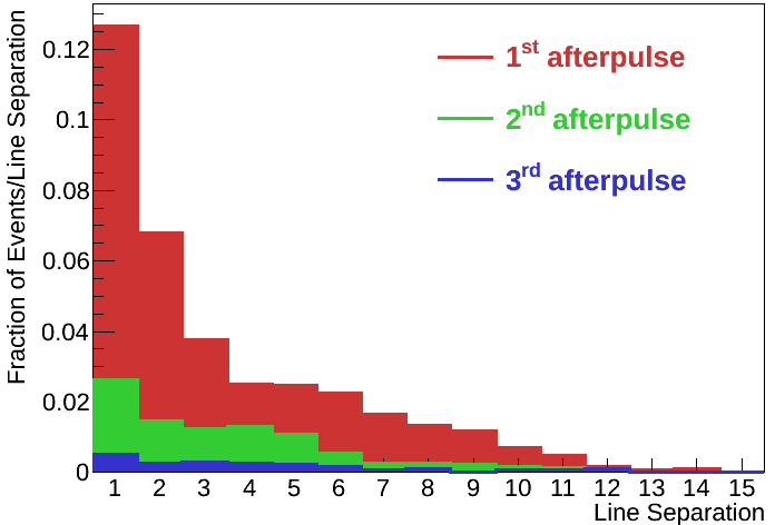
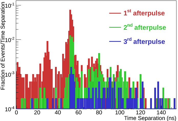
The number of secondary (, , , etc.) hits in a line decreased with distance from the primary hit location as shown in Figure 15. This shows that afterpulses and the discharge spreading are decreasing rapidly after the third line 7.5 mm away from the primary pulse. Although the secondary hits appeared mostly on a time scale of 100 ns or less, as shown in Figure 16, this did not preclude longer time scale processes such as metastable states or ion drift from initiating discharges.
4.2.3 Arrival time
The arrival time of the signal relative to the trigger was measured. Arrival time=0 corresponds to the passage of the muon through the panel. The important parameters of the signal time distribution are the mean, i.e. the discharge formation time, and the width, i.e. the fluctuation in the discharge formation time, that limited the timing resolution of the detector.
Cosmic ray muon data were acquired with different gas mixtures and pressures, and over a range of applied HV. Figure 17 shows the mean and Gaussian width of the muon arrival time distribution for various operating conditions.
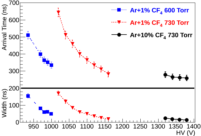
The arrival time resolution, represented by the Gaussian width decreased as the HV increased. In these measurements no trigger timing data were available, so the effective time resolution was widened by the 25 ns least count timing of the data acquisition. In any case the effect of voltage with various gas mixture and pressures is clearly visible in Figure 17: the gas mixture with higher concentration of CF4 yields faster timing.
Additional measurements were performed in which trigger time information was available. They displayed a trigger timing jitter of ns measured as the sigma of a Gaussian fit of the time difference between the two trigger scintillators. Figure 18 shows a cosmic ray muon arrival time distribution made with this trigger time subtraction. This measurement used a gas mixture of 20% CF4 in 3He at 730 Torr operated at 1035 volts. An intrinsic time resolution of ns was determined by fitting the primary arrival time peak, and after accounting for the trigger timing jitter.

4.2.4 Cosmic ray muon efficiency estimation
A panel’s sensitivity to MIPs can be estimated from cosmic ray muon detection experiments. For this purpose three definitions of efficiency were used:
-
1.
A raw efficiency, , was the ratio of the number of detected cosmic ray muons to the number of triggers:
(1) where was the number of trigger and PPS coincidences.
-
2.
A panel efficiency, was defined by and estimated from:
(2) where was the fractional acceptance, taken as the ratio of the instrumented panel area relative to the total trigger area. .
-
3.
A pixel efficiency was defined and estimated by,
(3) where was the pixel packing fraction given in Table 1.
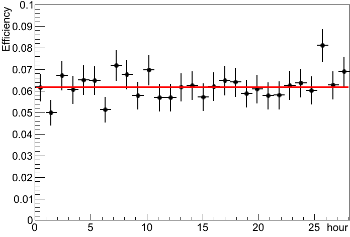
The panel efficiency of these modified display panels was about 6% to 13%, depending upon the HV, limited by the very thin gas gap and the small pixel packing fraction. Figure 19 shows an example of the panel efficiency for a gas mixture of 1% CF4 in Ar at 600 Torr. These data showed a stable muon detection rate over a 28 hour run.
The pixel efficiency was the efficiency for a single pixel to discharge when an ionizing particle traverses it. A few considerations affected the estimation of the pixel efficiency:
-
1.
The trigger rate was uniform across the entire triggering area.
-
2.
Only the pixel area was active with no significant fringe or edge effects. The effective pixel size did not increase with the applied voltage. The active area of a panel was determined by the packing fraction, estimated for a VPA panel to be 23.5% (Table 1).
-
3.
The average number of primary ion pairs, NP, was Poisson distributed. Using Ar as the host gas with 10% CF4 [25] and a gas gap of m, a cosmic ray muon passing through the tested panel produced an average of 0.95 ion pairs. The Poisson probability for a MIP to produce at least one ion pair in the panel was:
(4)
The maximum possible efficiency for detecting a MIP in a single cell of these panels was 0.61, limited by the probability to generate at least a single ion-pair in the thin gas gap.
The panel efficiency and the single pixel efficiency based on the above assumptions are shown in Figure 20 as a function of operating voltage.
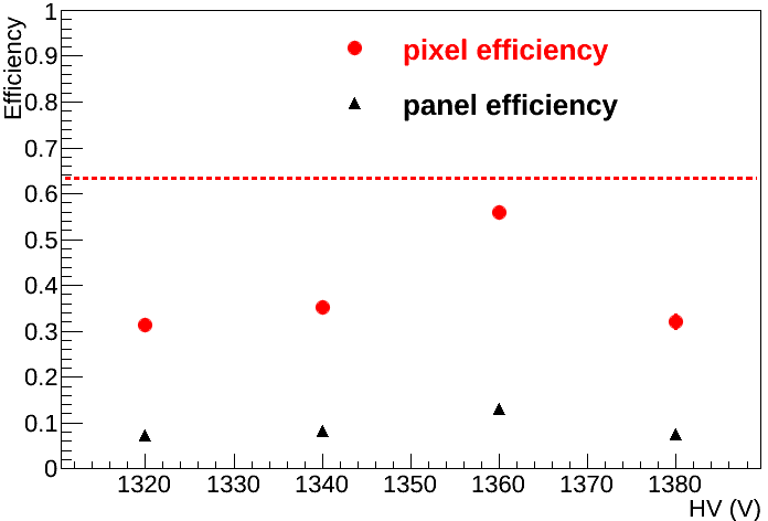
For the VPA panel, filled with 10% CF4 in Ar at 730 Torr and operating at 1360 volts, the pixel efficiency was 55%, which was nearly 90% of the maximum possible efficiency of 61%. The observed efficiency rise with voltage is expected. The drop off at 1380V is a consequence of dead time caused by numerous pixels firing spontaneously at very high rates.
4.3 Position measurements and spatial resolution
In order to investigate the panel’s position sensitivity and estimate position resolution, a series of position scan measurements were done. In these measurements the relative position of a collimated radioactive source with respect to the PPS readout electrodes was reconstructed. A large working area was instrumented consisting of 20 readout lines 30 HV lines. The collimated radiation source produced hit distributions. Fits to these hit distributions yielded a measure of the source position.
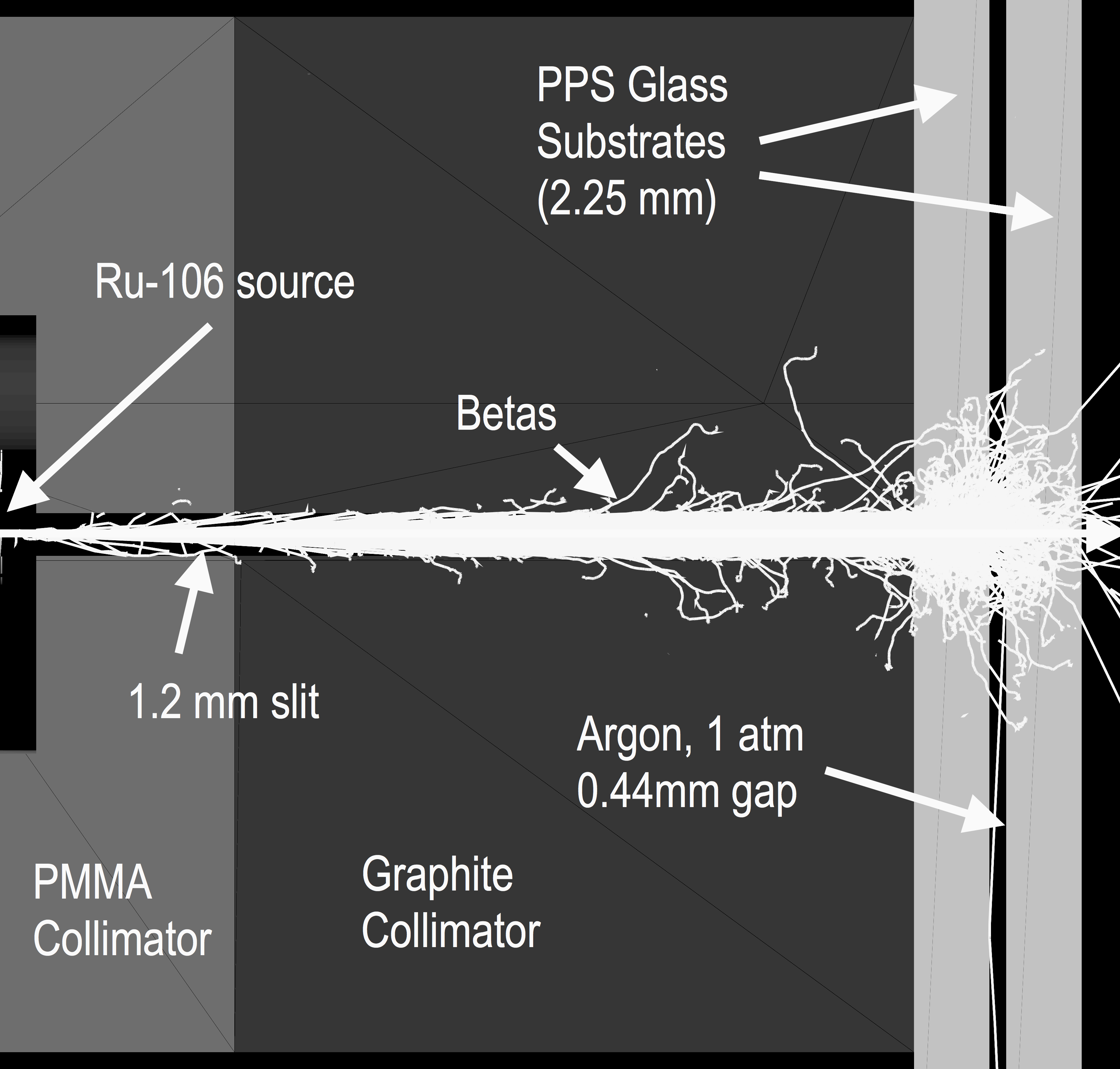
A computer controlled robotic arm mounted on an X-Y translatable axis performed automated position scans. A collimated 106Ru source was attached at one end of the arm and positioned over the panel. The collimator consisted of a 2 cm thick graphite block with a 1.25 mm slit aperture between the source and glass substrate. Control software translated the source in both X and Y directions with a precision of about 2 m. At each step of the position scan, data were acquired for equal time intervals and signals from each readout channel were counted with a 20 channel scaler.
4.3.1 Simulation of the collimated source
The investigation of the spatial response of the panel was augmented by a Monte Carlo simulation of the source collimation and PPS material scattering. GEANT4 [26] simulations were used to evaluate the contribution of the scattering of the source electrons to the measured distribution of betas in the detector. The full simulation started with the energy spectrum of the bare isotope, included scattering in the ceramic matrix within which the isotope was deposited, the collimator material and aperture, and the glass substrates of the panel. The emission of s was in all directions, sampled appropriately from the energy distribution. The limited sampling in Figure 21 shows the effect of the air scattering, the effectiveness of the collimation and the glass energy loss and dispersion, using a pencil beam sampled from the energy distribution. s entering the panel experienced significant scattering and absorption in the front glass substrate, so much so that few were able to exit the panel through the back glass substrate.
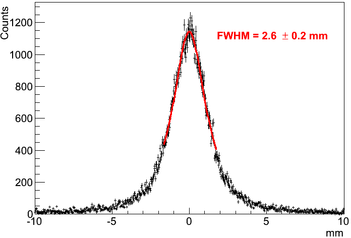
The initial 1.25 mm collimated beam of particles had spread at the entrance of the discharge gas volume to a distribution with full width at half maximum (FWHM) of about 2.6 mm with long non-Gaussian tails, as shown in Figure 22. The resulting “collimated” beam inside the PPS thus also illuminated adjacent sense electrodes on each side of the targeted electrode under the graphite slit.
4.3.2 Spatial resolution determination from data
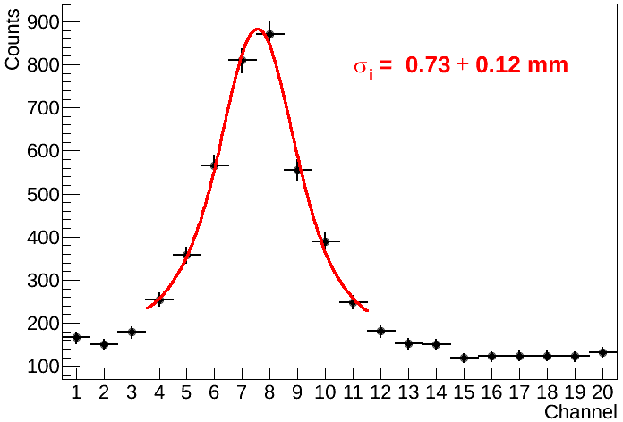
The intrinsic resolution was estimated from the convolution fit of the panel hit distribution using a Gaussian to represent the intrinsic resolution and a Breit-Wigner function that well described the Monte Carlo distribution around the peak region. Figure 23 displays the result of a single position scan run, using the 106Ru source and acquiring data for 20 minutes at each point. The intrinsic resolution obtained for the 1 mm pixel pitch panel in Figure 23 was mm.
This approach yielded an upper limit to the resolution because it ignored three systematics.
One was the absence of secondary s in the simulations. These secondaries originated from the conversion of s (e.g., X-rays shown in Figure 21). While expected only at the few percent level, these s produced a very broad distribution and were superimposed on the distribution from primary s.
A second systematic effect arose from the lack of timing information in the readout method employed for these tests. In this open architecture panel about 1/3 of the hits yielded an afterpulse within a few tens of sec. These afterpulses were mostly vetoed and did not register as hits. Nevertheless, less than 5% of the afterpulses incremented a scaler channel before the veto was applied.
The third systematic omission was that the simulation generated the distribution of s at the entrance to the gas volume. This fails to account for the large angular distribution of the particles introduced by multiple scattering in the air column and in the glass, which would cause the distribution to spread significantly as it propagates through the gas volume.
In general, for each complete scan, the hit map from each step was fitted with a Breit-Wigner plus linear function to model the peak and long tails of the distribution. The position of the source, as seen by the detector, was then taken to be the value of the mean of the fit function. Figure 24 shows reconstructed source positions for a series of 100 m steps from a single position scan.
4.3.3 Medium energy protons
In addition to the described position resolution results from a particle source, similar results were obtained using a proton beam. A type VPA panel was exposed to a collimated, 226 MeV proton beam from an IBA C-235 proton beam therapy accelerator. An experiment using the 1 mm diameter beam, with an intensity of particles/sec-mm2 demonstrated the beam position measurement to be consistent with the 2.5 mm pixel pitch [27].
4.4 Neutron detection
In collaboration with Reuter-Stokes (General Electric Co.) in Twinsburg, OH, a prototype PPS was evaluated as a detector capable of neutron detection with a low gamma ray interaction rate. A 2.5 mm pitch panel was filled with a gas mixture of 80% 3He and 20% CF4 at 730 Torr. Some 600 instrumented pixels, almost 39 cm2, were exposed to thermal neutrons produced by various neutron sources (i.e., 252Cf, 241Am-Be and 239Pu-Be). The sources were encapsulated and nested in the center of a cylinder of high density polyethylene.
Hit rate measurements were performed with and without a 10B-Al neutron mask between the source and the panel. The borated aluminum mask was 7.75 mm thick, and had a 10B areal density of mg/cm2. 10B has a cross section of 3835 Barns for thermal neutrons. A calculation of thermal neutron transmission based on the above values yields 0.001%. The transmission of gammas is calculated to be 70%-80%. A GE proprietary measurement determined that at most 0.1% of the source generated neutrons were transmitted by the mask.
The thermal neutron capture on 3He resulted in the emission of a low energy proton and a triton, sharing a total kinetic energy of 764 KeV. Since the interaction occurred essentially at rest, these particles were emitted isotropically, with a range of 1 to 2 cm in the gas mixture of the panel. They were very highly ionizing, producing many hundreds of ion-pairs in the panel gas gap.
Results of two sets of measurements with and without the neutron source at different HV values are shown in Figure 26. After subtracting the contribution to the total rate, a plateau was observed in the measured neutron rate above 1015 volts.
The expected thermal neutron hit rate was calculated as:
| (5) |
where is the 3He thermal neutron absorption cross section at 0.025 eV = barns [28]; was the instrumented panel area (); and based on the density of in the panel under lab conditions; and was the thickness of the panel gas gap. The thermal neutron flux incident on the instrumented region of panel, , was determined by a detailed GEANT4 MC calculation, and also with a direct measurement. The former yielded a flux of (statistical) Hz cm-2, and the latter Hz cm-2. The measurement error was dominated by an estimated 10% systematic uncertainty. The measured flux value was used. The factor represented the efficiency to detect the low energy breakup fragment passing through the instrumented area of the panel.
Using Eq. 5 with the above values for the tested configuration the calculated rate was Hz. The measured rate at the last point of Figure 26 was Hz. The comparison of the predicted and measured rates suggests that, within an error dominated by the measurement of the thermal neutron flux, the net efficiency, , to detect the captured neutron breakup fragments was consistent with unity. The absolute efficiency for thermal neutron detection was
| (6) |
The error was dominated by systematic uncertainty of the thermal neutron flux at the panel. The low efficiency was due to the minute amount of 3He at low pressure in the 0.38 mm gas gap. By comparison, a commercial neutron counter [29] with a 25 mm radius tube and pressurized with 3He to 4 atm has an efficiency for thermal neutrons of 62%.
Low sensitivity for detection is a desirable attribute of neutron detectors. A measurement of the panel efficiency for particles was conducted by directly irradiating the panel with an intense source, 137Cs with an activity of 8.5 mCi, set at a distance such that the panel received a rate of /sec () over the instrumented region. Table 2 reports the results for the -efficiency and corresponding neutron efficiency for a selection of HV settings. While this efficiency is not considered low [30], it can be further reduced principally by using thinner substrates, “thin-film” rather than thick-film electrodes and by reducing the thickness of the dielectric around each pixel.
| HV(V) | -efficiency | n-efficiency | ratio |
|---|---|---|---|
| 970 | |||
| 1000 | |||
| 1030 |
In a final test intended to evaluate position sensitivity to thermal neutrons, a 10B-Al neutron mask with a 5 mm wide slit was interposed between the neutron source and the panel. The source was located far from the slit aperture, at a distance much larger than the slit width, to approximate a uniform flux of neutrons and s incident on the panel. The resulting distribution in Figure 27 shows a peak over a much smaller background. The Gaussian plus linear fit gives a sigma of 1.11 readout lines, or 2.8 mm. The corresponding FWHM is 6.6 mm, in rough agreement with the 5 mm of the slit dimension.

5 Summary
This research was intended to demonstrate the potential of the plasma panel sensor as an inexpensive, hermetically sealed, scalable, high resolution and granularity, fast timing, high performance detector for a variety of sources and applications, even in an intense radiation and magnetic field environment. Test results on prototypes, adapted directly from commercial monochromatic plasma display panels, are reported here. Pulses induced in the panels were systematically characterized, expanding on previously reported laboratory results [27, 31, 32, 33]. The results showed that high gain, fast time response, high spatial resolution and high granularity are achievable. The first prototype detectors successfully measured minimum ionizing particles, betas, protons, gammas and thermal neutrons from radioactive sources. Spatial resolution comparable with the pitch of the device and a time resolution as fast as 2 to 3 ns was measured. We are now investigating devices using discharge cells with better cell physical and electrical isolation, a longer drift space and higher fill factors. This should lead to a reduced level of discharge spreading, lower capacitance and faster discharge times (nanoseconds or lower) and very high position resolution. Deeper cells with longer interaction paths will increase the detector efficiency. Finally, the transition to devices fabricated using much thinner substrates will enhance transmission of highly ionizing particles while reducing secondary particle and photon generation.
Acknowledgment
Development of the PPS project was funded by the U.S. Department of Energy (DOE) - Office of Nuclear Physics Small Business Innovation Research grant award numbers DE-SC0006204 and DE-FG02-07ER84749 to Integrated Sensors, U.S. DOE, Office of Nuclear Physics, Applications of Nuclear Science and Technology grant to Oak Ridge National Laboratory, operated by UT-Battelle, LLC for the U.S. DOE, and DOE - Office of High Energy Physics grant number DE-FG02-12ER41788 to the University of Michigan. The research at Tel Aviv University was supported by the I-CORE Program of the Planning and Budgeting Committee and the Israel Science Foundation (grant number 1937\12). Funding for scientific exchange and collaboration between Tel Aviv University and the University of Michigan was provided by the Israel-American Binational Science Foundation, grant number 1008123.
Disclaimer: This report was prepared as an account of work sponsored by an agency of the United States Government. Neither the United States Government nor any agency thereof, nor any of their employees, makes any warranty, express or implied, or assumes any legal liability or responsibility for the accuracy, completeness, or usefulness of any information, apparatus, product, or process disclosed, or represents that its use would not infringe privately owned rights. Reference herein to any specific commercial product, process, or service by trade name, trademark, manufacturer, or otherwise does not necessarily constitute or imply its endorsement, recommendation, or favoring by the United States Government or any agency thereof. The views and opinions of authors expressed herein do not necessarily state or reflect those of the United States Government or any agency thereof.
References
- [1] D.S. Levin et al., “Development of a plasma panel muon detector” Nuclear Instruments and Methods in Physics Volume 652, Issue 1, 1 October 2011, Pages 315-318, ISSN 0168-9002, http://dx.doi.org/10.1016/j.nima.2010.07.076
- [2] P.S. Friedman et al., “Large-Area Plasma-Panel Radiation Detectors for Nuclear Medicine Imaging to Homeland Security and the Super Large Hadron Collider”, International Display Symposium, Seattle, WA, May 2010, arXiv:1007.0487v1 [physics.ins-det]
- [3] R. Ball et al., “Plasma Panel Detectors for MIP Detection for the SLHC and a Test Chamber Design”, IEEE Nuclear Science Symposium Conference Record, Orlando, (2009) 1321-1327 arXiv:1007.0486 [physics.ins-det]
- [4] P. S. Friedman, “A New Class of Low Cost, High Performance Radiation Detectors”, 2005 IEEE NSS-MIC Conference Record, pp. 2815-2822
- [5] P. S. Friedman and R.A. Stoller, US Patents 7,332,726 (2008), 7,518,119 (2009), 7,564,039 (2009), 7,683,340 (2010), 7,696,485 (2010), 7,902,516 (2011), 7,982,191 (2011), 8,158,953 (2012), 8,389,946 (2013) and 8,710,449 (2014)
- [6] R. Ball et al., “Progress in the Development of Plasma Panel Radiation Detectors”, IEEENuclear Science Symposium Conference, (Knoxville, TN), Paper N50-7 (November 3, 2010) arXiv:1101.0045 [physics.ins-det]
- [7] J. P. Boeuf “Plasma display panels: physics, recent developments and key issues”, J. Phys. D: Appl. Phys. 36 (2003) R53R79 (February 2003)
- [8] Glenn F. Knoll “Radiation detection and measuremen”, fourth edition, ISBN: 978-0-470-13148-0
- [9] M.J. Druyvesteyn and F.M. Penning “The Mechanism of Electrical Discharges in Gases of Low Pressure” Rev. Mod. Phys. 12 (1940) 87 [Erratum ibid. 13 (1941) 72]
- [10] A. V. Phelps and J. P. Molnar “Lifetimes of Metastable States of Noble Gases” Phys. Rev. 89, 1202–1208 (1953)
- [11] H. Raether, Zeits. f. Physik 112, 464 (1939)
- [12] J. M. Meek, “A Theory of Spark Discharge”, Physical Review V.57 (1940)
- [13] M. Atac, A.V. Tollestrup, D. Potter, “Self-quenching Streamers” Nuclear Instruments and Methods 200 345 (1982)
- [14] COMSOL Multiphysics. [Online] COMSOL Inc. http://www.comsol.com/products/multiphysics
- [15] http://www.home.agilent.com/
- [16] L. W. Nagel and D. O. Pederson, “SPICE (Simulation Program with Integrated Circuit Emphasis)”, Memorandum No. ERL-M382, University of California, Berkeley, Apr. 1973
- [17] PSI DRS Chip Home Page: http://drs.web.psi.ch
- [18] Y.Arai et al., “ATLAS Muon Drift Tube Electronics” 2008 JINST 3 P09001, http://iopscience.iop.org/1748-0221/3/09/P09001
- [19] http://www.wiener-d.com/sc/modules/nim–modules/nimbox-npl20.html. A custom firmware for the 4 units allowed the use of all 20 NIM inputs as scalers.
- [20] http://www.caen.it/csite/CaenProd.jsp?parent=11&idmod=62
- [21] http://www.ni.com/labview/
- [22] Rene Brun and Fons Rademakers, “ROOT - An Object Oriented Data Analysis Framework”, Proceedings AIHENP’96 Workshop, Lausanne, Sep. 1996, Nucl. Inst. & Meth. in Phys. Res. A 389 (1997) 81-86. See also http://root.cern.ch/
- [23] www.nucleide.org/DDEP_WG/Nuclides/Sr-90_tables.pdf
- [24] A. Munoz et al., “Energy deposition model based on electron scattering cross section data from water molecules”, Journal of physics: Conference Series 133 (2008) 012002, doi:10.1088/1742-6596/1331/1/012002
- [25] A.Sharma “Transport Properties of operational gas mixtures used at LHC” SLAC-JOURNAL-ICFA-16 (1998)
- [26] S. Agostinelliae et al.,“Geant4—a simulation toolkit”, Nuclear Instruments and Methods in Physics Research Section A: Accelerators, Spectrometers, Detectors and Associated Equipment Volume 506, Issue 3, 1 July 2003, Pages 250-303
- [27] P. S. Friedman et al., “Plasma Panel Sensors for Particle and Beam Detection”, 2012 IEEE NSS-MIC Conference Record, pp. 1775-1780
- [28] J. Als-Nielsen and O. Dietrich “Slow Neutron Cross Sections for , B and Au” Physical Review, vol. 133, Issue 4B, pp. 925-929
- [29] http://www.ge-mcs.com/download/reuter-stokes/GE_14158_L.pdf
- [30] United States Government Accounting Office, “ Neutron Detectors”, report GAO-11-753 Sept. 2011
- [31] Peter Friedman et al., “Plasma Panel-Based Radiation Detectors”, J. Soc. Info. Display, 21/1 (2013), pp. 46-54 (doi: 10.1002/jsid.151),http://arxiv.org/abs/1305.2277.
- [32] Silver, Y. et al. “Development of a Plasma Panel Radiation Detector: Recent Progress and Key Issues” 2011 IEEE NSS-MIC Conference Record pp. 1881-1885, (doi: 10.1109/NSSMIC.2011.6154379)
- [33] R. Ball et al., “Plasma Panel Detectors for Ionizing Particles”, Snowmass 2013 Instrumentation Frontier Whitepapers, http://www.snowmass2013.org/tiki-download_file.php?fileId=67.