Graphene optomechanics realized at microwave frequencies
Abstract
Cavity optomechanics has served as a platform for studying the interaction between light and micromechanical motion via radiation pressure. Here we observe such phenomena with a graphene mechanical resonator coupled to an electromagnetic mode. We measure thermal motion and back-action cooling in a bilayer graphene resonator coupled to a microwave on-chip cavity. We detect the lowest flexural mode at 24 MHz down to 50 mK, corresponding to roughly mechanical 40 quanta, representing nearly three orders of magnitude lower phonon occupation than recorded to date with graphene resonators.
Graphene can be considered as an ultimate material for studying the quantum behavior of the motion of micromechanical resonators. It is lightweight, and therefore the zero-point motion of a particular mode of frequency and mass is unusually large. It is stiff, such that the frequency is high for a given mass, allowing for approaching the quantum limit in dilution refrigerator temperatures. Moreover, graphene resonators can portray appreciable nonlinearity at single-quantum level. These properties would make graphene attractive for the use in cavity optomechanics experiments.
In the field of cavity optomechanics Aspelmeyer and Marquardt (2013), remarkable findings have been made during the last ten years. These include, for example, ground state cooling of a mechanical mode Teufel et al. (2011); Chan et al. (2011). Briefly, an optical or more generally electromagnetic cavity mode with a movable mirror or boundary condition allows to couple the confined photons and the motion by means of the radiation pressure exerted by the photons.
Photothermal interaction between the motion of a mechanical resonator made with graphene Bunch et al. (2007); Garcia-Sanchez et al. (2008); Xu et al. (2010); Lee et al. (2013) and light was observed quite recently Barton et al. (2012). These authors had a on-chip trench covered by graphene, thus forming the cavity. However, since the graphene end mirror is 98 % transparent, the -value was much less than one, and canonical radiation pressure phenomena could not be observed.
In contrast to optical frequencies, graphene naturally lends itself to microwave-frequency cavities as it is opaque at these frequencies. The driven motion of a graphene mechanical resonator was observed by coupling to an off-chip tank circuit Song et al. (2012), however, the coupling was not sufficient to observe graphene thermal motion not to mention cavity back-action.
In this work we make the first demonstration of radiation pressure effects on the motion of graphene in the context of cavity optomechanics. Cooled in a dilution refrigerator, we study the lowest drum-like flexural mode of a bilayer graphene resonator at MHz, coupled to a high- microwave cavity resonator. We observe thermal motion down to 70 mK, furthermore, we carry out cavity back-action sideband cooling to further dampen the effective mode temperature down to 50 mK. A thermal transport model is developed to explain the findings.
The interaction of a mechanical resonator with a microwave-regime electrical cavity is similar to the radiation pressure force; displacement affects the cavity frequency . This is naturally described in terms of an equivalent capacitance of the cavity, and a movable capacitance of the conductive mechanical part. The coupling energy, that is, how much the zero-point motion displaces the cavity frequency, is given by .
Since for a plate capacitor , a narrow vacuum gap is instrumental for obtaining a high . Although also grows with surface area of the membrane, the dependence is linear and thus our design emphasizes a small gap. A small size in the low micron-range gives the benefit that the frequency is higher (tens of MHz) and quantum limit more easily attainable than with a large-size design.
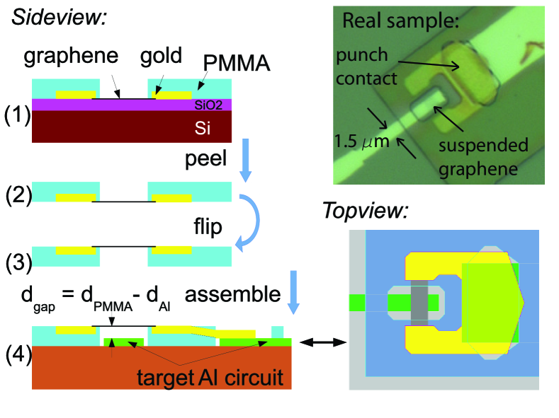
We have developed a technique to fabricate narrow gaps nm for a membrane about 2.5 m long and 1.5 m wide in a bridge geometry. First, high-quality tape-exfoliated bilayer graphene pieces are located on a silicon substrate covered with 275 nm thick SiO2 and confirmed with Raman spectroscopy. After the lithography and transfer process illustrated in Fig. 1, the other end of the gold contact is punched down well in contact to the other aluminum electrode over an area of m. Since we have a good control of the thickness of the aluminum electrode nm as well as that of the PMMA stamp nm, the vacuum gap is determined as nm.
Although the punch from gold to aluminum breaks the Al oxide, a galvanic contact between Au and Al is not established since the Al immediately oxidizes. Hence, the graphene is electrically floating. However, the capacitance between Au and Al satisfies such that the coupling is fully determined by the movable capacitance . We expect the charge density of the graphene to be low and its resistance thus to be high k.
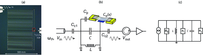
The cavity is a mm-size meandering design made out of aluminum on high-purity silicon chip (Fig. 2a). Since both ends of the cavity are floating, the effective capacitance in the circuit schematics (Fig. 2b) is very low given the dimensions, fF. We can convert the real circuit in Fig. 2b into an equivalent parallel resonator (Fig. 2c) where the graphene resistance is included in . With the current parameters , the effective capacitance essentially equals . Also, the external and purely cavity losses .
From the parameters of the graphene and the cavity, we obtain a prediction for the coupling of the lowest flexural mode Hz. However, the data is best fitted (see below) by clearly lower Hz. We attribute this to a tendency of the membrane mode shape to be distorted by non-uniform strain at the clamps.
The measurements are carried out in a dilution refrigerator down to 22 mK base temperature. We measure transmission of near-resonant microwaves through the cavity. In the data discussed here, we apply pump microwave irradiation at the red motional sideband frequency . The cavity linewidth below 350 mK is found as MHz. This is set by the effective resistance of the graphene (Fig. 2c), thus reducing the -value of the cavity. This finding is consistent with about k total resistance of the graphene.
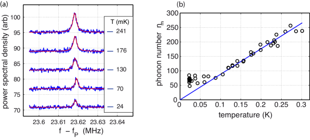
The information on the mechanical resonator appears in the motional sidebands spaced about the pump frequency. In Fig. 3a we show results for such a measurement which depict the thermal motion of the lowest mode of the suspended graphene. We used such low pump power that the cavity back-action damping (see below) had a negligible effet. The mechanical -value at the base temperature was about .
As clear in Fig. 3a, the height of the peaks grows with temperature. Ideally, the peak area is linearly proportional to cryostat temperature , since by equipartition, . Since it is very difficult to estimate with reasonable error bars everything affecting the peak height, such as cable attenuation, amplifier gain, or cavity internal losses, we follow the usual practice and calibrate the transduction between peak area and phonon number by relying on the linear temperature dependence, here obeyed above about mK as seen in Fig. 3b. We thus conclude that the lowest flexural mode thermalizes down to 70 mK in this experiment. This represents three orders of magnitude lower phonon occupancy than previous observations of graphene thermal motion, made at room temperature Bunch et al. (2007).
Sideband cooling owing to the radiation pressure interaction has been an extremely powerful and popular tool for studying micromechanical motion Gigan et al. (2006); Schliesser et al. (2009); Rocheleau et al. (2010); Teufel et al. (2011); Chan et al. (2011); Massel et al. (2012). Here, the pump microwave has to be applied at the red sideband, . This pump condition is similar to that used in the mere detection of the thermal motion as in Fig. 3, but now the pump power is orders of magnitude stronger. The sideband cooling process results in an enhanced effective damping experienced by the mechanical mode: , where . The total damping then gives a reduced phonon occupation: . Here, the thermal phonon number is set by the bath at the temperature according to . Although ideally the bath equilibrates at the cryostat temperature, in the following we find that the microwave heating causes that .
In the measurement, we indeed observe the thermal motion peak becoming broader as the pump power is increased (Fig. 4a), consistent with pure microwave radiation pressure interaction between the cavity and graphene. However, the height of the peaks grow progressively larger. We attribute this to an enhanced temperature of the environment experienced by the graphene mechanical mode. We can first extract the phonon number from the Lorentzians in Fig. 4a, showing progress of the sideband cooling in Fig. 4b. The cooling process clearly deviates from the ideal picture, and shows unusual non-monotonic behavior. Knowing and , we can also deduce the environmental phonon number (Fig. 4d). A relatively weak dependence of the temperature on microwave power hints that there is strongly temperature-dependent bottleneck setting the contact of the flexural mode to its bath.
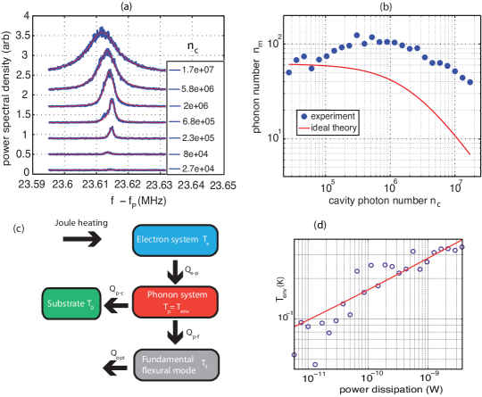
We can describe the mode temperature with a thermal model (Fig. 4c) of the chip at a cryostat temperature . We start by supposing the graphene electrons heat by Joule heating by microwave currents. Because the graphene is electrically floating, heat flow out from the electrons is entirely due to electron-phonon coupling. The phonons are scattered into the substrate across the relatively large contact area, the corresponding heat flow being . We also suppose the thermal environment of the lowest flexural mode is set by the phonon bath which couples via mechanical nonlinearities. The mode temperature is also affected by the sideband cooling with heat flow . In a typical case here, .
At low-temperatures , assuming parabolic bands McCann (2006), the electron phonon coupling in bilayer graphene can be written as Viljas and Heikkila (2010): , where is the graphene area, is a coupling constant, and denotes the phonon bath temperature. The coupling coefficient reads then , where eV is the deformation potential, eV denotes the interlayer coupling, the chemical potential, kg m-2 the mass density, m/s the Fermi velocity, and m/s the speed of sound Efetov and Kim (2010). On the basis of gate sweeps on similar samples, we estimate the residual charge density cm-2 which corresponds to chemical potential 17 meV. This yields K4Wm-2, which has been verified experimentally in Ref. Yan, 2012. At the largest electronic heating of nW (Fig. 4d), the weak electron-phonon coupling results in K.
The phonon temperature is bottlenecked by the Kapitza thermal boundary resistance between the graphene and gold. The present experiment allows for accurate measurement of this important quantity, not performed previously in dilution refrigerator temperatures. The data in Fig. 4d is fitted as , where the Kapitza conductivity WK-4m-2, and m2 is the contact area.
For 3d systems the following temperature dependence for the Kapitza conductivity is expected: . In thin films, the density of phonon modes is different, and often an exponent between 3-4 is observed Swartz and Pohl (1989). In graphene-metal systems, the temperature dependence of has been determined down to 50 K Schmidt et al. (2010); Balandin (2011) but not below; similar values have been obtained for graphene-SiO2 interfaces Chen et al. (2009) but there coupling to interfacial modes has been found to be important as well Freitag et al. (2009). Consequently, only rather crude estimates are available: we employ the results of Refs. Schmidt et al., 2010; Chen et al., 2009, extended by diffuse mismatch model Duda et al. (2009) to the asymptotic region with dependence. This yields for Kapitza conductance values two orders of magnitude smaller than that obtained from fitting to Fig. 4d but much larger than . Hence, the graphene-substrate thermal contact seems better than expected from theory.
We now turn the discussion into the limitations and prospects of our scheme. In nearly all optomechanics experiments, high internal -value of the cavity is favored. Although the graphene-induced dissipation in the cavity has a negative effect for the internal , we note that the present demonstrations presumably do not suffer much from this. We believe that losses due to graphene can be avoided to some extent by careful impedance design of the cavity and graphene contacts, by introducing a possibility for tuning the graphene charge density, or by proximitizing the graphene to be superconducting.
It is intriguing to further estimate the prospect of ground-state cooling, quantified usually as , of the mechanical modes of graphene relying on microwave radiation pressure. By increase of coupling one obtains, at a given bath temperature set by pump strength , higher damping and thus more efficient cooling. We obtain that a coupling Hz would be enough to cool to the ground state in the present setting. In fact, the ideal coupling in the present case is not too far from here, however, the measured value was about three times smaller. We take the same reduction factor and thus we need an ideal Hz. We suppose now a pristine monolayer graphene having the same dimensions as presently, but a narrower vacuum gap nm. The cavity capacitance can further be reduced down to fF by using low-dielectric substrate such as quartz Massel et al. (2011). With these realistic values, we obtain the required coupling and excellent prospect to reach the quantum ground state of moving graphene.
Acknowledgements We thank Erno Damskägg, Tero Heikkilä and Juha Pirkkalainen for useful discussions. This work was supported by the Academy of Finland, by the European Research Council (240387-NEMSQED) and by FP7 grant 323 924 iQUOEMS. The work benefited from the facilities at the Micronova Nanofabrication Center and at the Cryohall infrastructure.
References
- Aspelmeyer and Marquardt (2013) T. J. Aspelmeyer, M. Kippenberg and F. Marquardt, arXiv:1303.0733 (2013).
- Teufel et al. (2011) J. D. Teufel, T. Donner, D. Li, J. W. Harlow, M. S. Allman, K. Cicak, A. J. Sirois, J. D. Whittaker, K. W. Lehnert, and R. W. Simmonds, Nature 475, 359 (2011).
- Chan et al. (2011) J. Chan, T. P. M. Alegre, A. H. Safavi-Naeini, J. T. Hill, A. Krause, S. Groblacher, M. Aspelmeyer, and O. Painter, Nature 478, 89 (2011).
- Bunch et al. (2007) J. S. Bunch, A. M. van der Zande, S. S. Verbridge, I. W. Frank, D. M. Tanenbaum, J. M. Parpia, H. G. Craighead, and P. L. McEuen, Science 315, 490 (2007).
- Garcia-Sanchez et al. (2008) D. Garcia-Sanchez, A. M. van der Zande, A. S. Paulo, B. Lassagne, P. L. McEuen, and A. Bachtold, Nano Letters 8, 1399 (2008).
- Xu et al. (2010) Y. Xu, C. Chen, V. V. Deshpande, F. A. DiRenno, A. Gondarenko, D. B. Heinz, S. Liu, P. Kim, and J. Hone, Appl. Phys. Lett. 97, 243111 (2010).
- Lee et al. (2013) S. Lee, C. Chen, V. V. Deshpande, G.-H. Lee, I. Lee, M. Lekas, A. Gondarenko, Y.-J. Yu, K. Shepard, P. Kim, et al., Appl. Phys. Lett. 102, 153101 (2013).
- Barton et al. (2012) R. A. Barton, I. R. Storch, V. P. Adiga, R. Sakakibara, B. R. Cipriany, B. Ilic, S. P. Wang, P. Ong, P. L. McEuen, J. M. Parpia, et al., Nano Letters 12, 4681 (2012).
- Song et al. (2012) X. Song, M. Oksanen, M. A. Sillanpää, H. G. Craighead, J. M. Parpia, and P. J. Hakonen, Nano Lett. 12, 198 (2012).
- Gigan et al. (2006) S. Gigan, H. R. Boehm, M. Paternostro, F. Blaser, G. Langer, J. B. Hertzberg, K. C. Schwab, D. Baeuerle, M. Aspelmeyer, and A. Zeilinger, Nature 444, 67 (2006).
- Schliesser et al. (2009) A. Schliesser, O. Arcizet, R. Riviere, G. Anetsberger, and T. J. Kippenberg, Nature Physics 5, 509 (2009).
- Rocheleau et al. (2010) T. Rocheleau, T. Ndukum, C. Macklin, J. B. Hertzberg, A. A. Clerk, and K. C. Schwab, Nature 463, 72 (2010).
- Massel et al. (2012) F. Massel, S. U. Cho, J.-M. Pirkkalainen, P. J. Hakonen, T. T. Heikkilä, and M. A. Sillanpää, Nat. Commun. 3, 987 (2012).
- McCann (2006) E. McCann, Phys. Rev. B 74, 161403 (2006).
- Viljas and Heikkila (2010) J. K. Viljas and T. T. Heikkila, Phys. Rev. B 81, 245404 (2010).
- Efetov and Kim (2010) D. K. Efetov and P. Kim, Phys. Rev. Lett. 105, 256805 (2010).
- Yan (2012) J. Yan, Nat. Nanotech. 7, 472 (2012).
- Swartz and Pohl (1989) E. Swartz and R. Pohl, Rev. Mod. Phys. 61, 605 (1989).
- Schmidt et al. (2010) A. J. Schmidt, K. C. Collins, A. J. Minnich, and G. Chen, J. Appl. Phys. 107, 104907 (2010).
- Balandin (2011) A. A. Balandin, Nat. Mater. 10, 569 (2011).
- Chen et al. (2009) Z. Chen, W. Jang, W. Bao, C. N. Lau, and C. Dames, Appl. Phys. Lett. 95, 161910 (2009).
- Freitag et al. (2009) M. Freitag, M. Steiner, Y. Martin, V. Perebeinos, Z. Chen, J. C. Tsang, and P. Avouris, Nano Lett. 9, 1883 (2009).
- Duda et al. (2009) J. C. Duda, J. L. Smoyer, P. M. Norris, and P. E. Hopkins, Appl. Phys. Lett. 95, 031912 (2009).
- Massel et al. (2011) F. Massel, T. T. Heikkilä, J.-M. Pirkkalainen, S. U. Cho, H. Saloniemi, P. J. Hakonen, and M. A. Sillanpää, Nature 480, 351 (2011).