Excitation and recombination dynamics of vacancy-related spin centers in silicon carbide
Abstract
We generate silicon vacancy related defects in high-quality epitaxial silicon carbide layers by means of electron irradiation. By controlling the irradiation fluence, the defect concentration is varied over several orders of magnitude. We establish the excitation profile for optical pumping of these defects and evaluate the optimum excitation wavelength of . We also measure the photoluminescence dynamics at room temperature and find a monoexponential decay with a characteristic lifetime of . The integrated photoluminescence intensity depends linear on the excitation power density up to , indicating a relatively small absorption cross section of these defects.
pacs:
78.55.-m, 78.47.jd, 61.72.jdSilicon carbide (SiC) has recently been suggested for deployment in various quantum technologies Baranov et al. (2005); Weber et al. (2010); Baranov et al. (2011); Koehl et al. (2011); Gali (2012a); Riedel et al. (2012); Baranov et al. (2013); Castelletto et al. (2013a). In particular, silicon vacancy () related defects can be used as coherently controllable Koehl et al. (2011); Soltamov et al. (2012) and selectively addressable Riedel et al. (2012); Falk et al. (2013a) qubits, characterized by long spin coherence and spin-lattice relaxation times even at room temperature. These atomic-scale qubits are also attractive for local sensing of magnetic Kraus et al. (2013) and electric Falk et al. (2013b) fields as well as temperature Kraus et al. (2013). Another potential use is as a low-noise quantum microwave amplifier based on the maser effect Kraus et al. (2014). Furthermore, SiC is a technologically friendly material, used in various devices (LED, MOSFETS, MEMS, sensors). This facilitates attractive opportunities for electrical control of these vacancy-related spin centers Fuchs et al. (2013); Klimov et al. (2013).
In all these appealing applications, an optical pumping scheme of the high-spin ground state of -related defects ( or ) Vainer and Il’in (1981); Wimbauer et al. (1997); Sörman et al. (2000); Mizuochi et al. (2002); Orlinski et al. (2003); Ilyin et al. (2006); Son et al. (2006); Kraus et al. (2014) is exploited. This pumping scheme is assumed to be similar to that of the nitrogen-vacancy (NV) defect in diamond Jelezko and Wrachtrup (2006). In spite of this similarity, the optical properties of the -related defects in SiC have not been measured in detail. It is worth noting that another vacancy centers in SiC, associated with the so-called AB lines, have been demonstrated to be very efficient single photon sources Castelletto et al. (2013b). In these single-defect experiments, the positively charged configuration of these centers has been investigated, which has low-spin ground state (). Therefore, it is unclear whether their quantum control is possible in the same manner as for the -related defects in SiC or the NV defect in diamond.
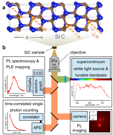
In this Letter, we measure excitation spectrum and recombination dynamics of in 4H-SiC at room temperature. The crystal structure of polytype 4H is shown in Fig. 1(a). There are four Si and four C atoms per unit cell with stacking sequence ABCB (where A, B and C denote close-packed atomic planes). The broken bonds with missing Si atom result in the appearance of additional energy states and the electron density is mostly localized at the first- (C) and second-neighbor (Si) atoms to this vacancy. According to the density functional theory (DFT) calculations Gali (2012b), the highest occupied state and the lowest (partially) unoccupied states lie deep in the forbidden gap of SiC, which is at room temperature. For this reason, these defects can be detected by their characteristic photoluminescence (PL) in the spectral range shifted towards longer wavelengths with respect to the fundamental emission/absorption edge (ca. in 4H-SiC). At cryogenic temperatures, the so-called zero-phonon lines (ZPLs) are observed, distinct in their optical transition energies. In highly homogeneous samples, these ZPLs are very sharp with full width at half maximum (FWHM) of a few (ref. Riedel et al., 2012). With rising temperature, the ZPLs are significantly broadened due to interaction with thermally excited phonons and their FWHM is approximately at .
In 4H-SiC there are two non-equivalent lattice sites and, therefore, there are two different defects with corresponding ZPLs labeled as V1 and V2 (ref. Wagner et al., 2000). These defects are probably perturbed by carbon vacancies Baranov et al. (2013), which are not shown in Fig. 1(a) for simplicity. When a silicon and carbon vacancies are situated along a chemical bond, a divacancy (-) is formed Baranov et al. (2005); Son et al. (2006), having its own ZPL.

The 4H-SiC samples investigated in this Letter have been purchased from CREE. A nominally undoped (residual n-type doping ) layer of thickness was epitaxially grown on a 2-inch n-type 4H-SiC wafer ( thickness, off-axis orientation). The layer is conserved by a 5--thick n-type 4H-SiC layer () and a 2--thick p-type 4H-SiC layer (). The wafer was diced in pieces. In order to create -related defects the samples were irradiated with electrons to different fluences.
First, we present spatial imaging of defects in our SiC samples [our microscopy setup is schematically sketched in Fig. 1(b)]. The sample is placed in an inverted Ti-U microscope and the PL is excited and collected through a 20x CFI Super Plan Fluor ELWD objective with (Nikon). The excitation light from a SuperK EXTREME (EXR-15) supercontinuum laser (NKT Photonics) was defocused onto a spot of approximately in diameter. The PL image in the confocal plane of the objective is recorded by a Clara interline CCD camera (Andor), with one CCD pixel () corresponding to at the sample position. The difraction-limited spatial resolution of the setup is about . We use a wide-band excitation () for imaging, and the emission is detected for longer wavelengths ().

To measure PL spectra we use a Shamrock SR-303i spectrograph (Andor) together with either a Newton CCD camera (DU920P-OE) for detection from to or a iDus InGaAs array detector (DU491A-1.7) for detection from to [Fig. 1(b)]. This configuration provides the spectral resolution of ca. . For photoluminescence excitation (PLE) measurements, the laser wavelength is selected from the supercontinuum spectrum with a step of using a SuperK VARIA bandpass filter (NKT Photonics). In low-temperature experiments (), the sample is mounted in a cold-finger MicrostatHe (Oxford Instruments) and placed in a LabRAM system for spectroscopy (Horiba Scientific). In this case we use a He-Ne laser () for excitation.
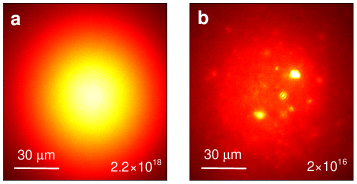
Figure 2 shows PL images of two samples irradiated with electrons to different fluences. The wavelength range detected by the PL microscope setup is associated with emission from color centers (below we demonstrate that these colour centres are the defects). At a high irradiation fluence (), the PL intensity appears to closely follow the excitation profile which suggests that emission is from a homogeneous distribution of color centers [Fig. 2(a)]. At a much lower irradiation fluence () this profile splits up into several more strongly emissive fragments [Fig. 2(b)]. Some of these fragments have sub- size and reveal diffraction rings. Neither of these is observed in as-grown samples suggesting that these color centers were produced by electron irradiation.

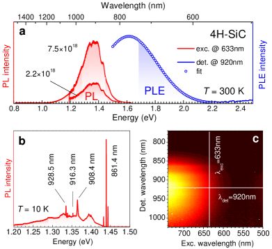
The room-temperature PL spectra are presented in Fig. 3(a). With increasing electron irradiation from to the integrated PL intensity increases ca. by a factor of three, suggesting that the defect concentration is proportional to the irradiation fluence. We observe PL in the spectral range from to , which is characteristic for in SiC at room temperature Fuchs et al. (2013). On the other hand, we do not observe PL in the spectral range from to , where PL from - is expected Koehl et al. (2011). By cooling down to we resolve four ZPLs in the PL spectrum [Fig. 3(b)]. The V1 ZPL at dominates in the spectrum, unambiguously proving that we generate and probe the defects.
In oder to find the optimal excitation conditions we perform PLE mapping experiments. First, we ascertain that the PL spectrum is independent of the excitation wavelength [Fig. 3(c)]. A PLE spectrum, detected at the PL maximum () and corrected for the laser supercontinuum spectrum, is presented in Fig. 3(a). With decreasing wavelength () the excitation becomes less efficient and for the PL is not excited. The corresponding energy is still significantly smaller than the bandgap in 4H-SiC (). According to the Franck-Condon principle, the PLE maximum is shifted towards higher energy with respect to the ZPL. In oder to estimate this maximum, we fit the PLE spectrum in Fig. 3(a). In fact, the PLE spectrum associated with vibronic bands in the crystal has a complex form and is usually asymmetric with respect to the maximum. We find that the high-energy tail of the experimentally obtained PLE spectrum () is perfectly described by the Gaussian in the form with and [open circles in Fig. 3(a)], indicating that inhomogeneous broadening dominates the excitation spectrum. Following this fit, the optimal excitation wavelength is around . Interestingly, we observe non-equivalent linewidth of the PL and PLE spectra, expected to be similar from a configuration coordinate diagram approach. A possible explanation could be due to the different interaction with phonons in the ground and excited states. Further understanding requires detailed theoretical consideration, which is beyond the scope of this work.
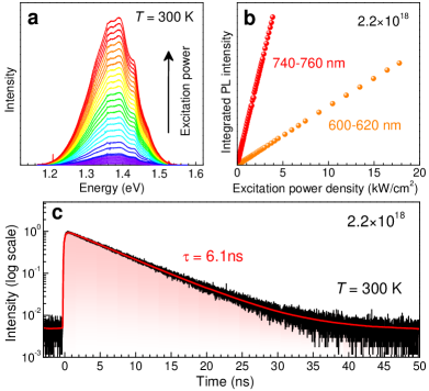
To estimate the excitation efficiency we measure the integrated PL intensity as a function of excitation power [Fig. 4(a)]. It is presented in Fig. 4(b) for two spectrally different excitations. The excitation in the spectral range is more efficient than in , as expected from the PLE spectrum of Fig. 3(a). We observe perfectly linear dependences on the excitation power density up to () and (), indicating that all the results reported here are obtained far below the saturation. Remarkably, the saturation power density for the NV defect is about (refs. Jelezko and Wrachtrup, 2006; Kurtsiefer et al., 2000). As we do not observe deviation from the linear dependence, this suggests that the absorption cross section of the defects is comparable or smaller than that of the NV defect.
Finally, we analyze PL dynamics of , using time-correlated single photon counting (TCSPC) measurements. The repetition rate of the pulsed () excitation is and the spectrally integrated PL signal is detected using a Si single-photon avalanche photodiode and a TCSPC HydraHarp module (PicoQuant) [Fig. 1(b)]. To characterize our setup we measure the instrument response function, using scattered light from the laser in the spectral range from to , and obtain the overall time resolution of .

The decay of the PL after pulsed excitation is presented in Fig. 4(c). The experimental data are perfectly fitted with a monoexponential decay of the form convoluted with the instrument response function. From the fit we find the PL lifetime . This is of an order of magnitude comparable to that of another color center in SiC ()Castelletto et al. (2013b) and of the NV defect in diamond ()Kurtsiefer et al. (2000). This similarity is expected because all these atomic-scale defects are isolated from the bulk bands and their optical transitions are determined by the coupling of the electronic and vibronic states. The transition rate in this case, as a rule, is smaller than for direct band-to-band transitions in semiconductor nanostructures, like colloidal quantum dots Klimov et al. (2000) and quantum wells Yakovlev et al. (2000).
Summarizing, we have performed spatial imaging of the defects, generated by electron irradiation in epitaxial 4H-SiC layer, and investigated their optical properties. In particular, we have found the optimal excitation conditions to optically pump these defects and we have measured their PL lifetime. This information is important to optimize quantum control of these defects, as required for various appealing applications.
This work has been supported by the Bavarian Ministry of Economic Affairs, Infrastructure, Transport and Technology as well as by the DFG under grant AS310/4.
References
- Baranov et al. (2005) P. G. Baranov, I. V. Il’in, E. N. Mokhov, M. V. Muzafarova, S. B. Orlinskii, and J. Schmidt, Journal of Experimental and Theoretical Physics Letters 82, 441 (2005).
- Weber et al. (2010) J. R. Weber, W. F. Koehl, J. B. Varley, A. Janotti, B. B. Buckley, C. G. Van de Walle, and D. D. Awschalom, Proceedings of the National Academy of Sciences 107, 8513 (2010).
- Baranov et al. (2011) P. Baranov, A. Bundakova, A. Soltamova, S. Orlinskii, I. Borovykh, R. Zondervan, R. Verberk, and J. Schmidt, Physical Review B 83, 125203 (2011).
- Koehl et al. (2011) W. F. Koehl, B. B. Buckley, F. J. Heremans, G. Calusine, and D. D. Awschalom, Nature 479, 84 (2011).
- Gali (2012a) A. Gali, Materials Science Forum 717-720, 255 (2012a).
- Riedel et al. (2012) D. Riedel, F. Fuchs, H. Kraus, S. Väth, A. Sperlich, V. Dyakonov, A. Soltamova, P. Baranov, V. Ilyin, and G. V. Astakhov, Physical Review Letters 109, 226402 (2012).
- Baranov et al. (2013) P. G. Baranov, V. A. Soltamov, A. A. Soltamova, G. V. Astakhov, and V. D. Dyakonov, Materials Science Forum 740-742, 425 (2013).
- Castelletto et al. (2013a) S. Castelletto, B. C. Johnson, and A. Boretti, Advanced Optical Materials 1, 609 (2013a).
- Soltamov et al. (2012) V. Soltamov, A. Soltamova, P. Baranov, and I. Proskuryakov, Physical Review Letters 108, 226402 (2012).
- Falk et al. (2013a) A. L. Falk, B. B. Buckley, G. Calusine, W. F. Koehl, V. V. Dobrovitski, A. Politi, C. A. Zorman, P. X. L. Feng, and D. D. Awschalom, Nature Communications 4, 1819 (2013a).
- Kraus et al. (2013) H. Kraus, V. A. Soltamov, F. Fuchs, D. Simin, A. Sperlich, P. G. Baranov, G. V. Astakhov, and V. Dyakonov, arXiv:1403.7741.
- Falk et al. (2013b) A. L. Falk, P. V. Klimov, B. B. Buckley, V. Ivády, I. A. Abrikosov, G. Calusine, W. F. Koehl, A. Gali, and D. D. Awschalom, arXiv:1311.6832.
- Kraus et al. (2014) H. Kraus, V. A. Soltamov, D. Riedel, S. Väth, F. Fuchs, A. Sperlich, P. G. Baranov, V. Dyakonov, and G. V. Astakhov, Nature Physics 10, 157 (2014).
- Fuchs et al. (2013) F. Fuchs, V. A. Soltamov, S. Väth, P. G. Baranov, E. N. Mokhov, G. V. Astakhov, and V. Dyakonov, Scientific Reports 3, 1637 (2013).
- Klimov et al. (2013) P. V. Klimov, A. L. Falk, B. B. Buckley, and D. D. Awschalom, Physical Review Letters 112, 087601 (2014).
- Vainer and Il’in (1981) V. S. Vainer and V. A. Il’in, Sov. Phys. Solid State 23, 2126 (1981).
- Wimbauer et al. (1997) T. Wimbauer, B. Meyer, A. Hofstaetter, A. Scharmann, and H. Overhof, Physical Review B 56, 7384 (1997).
- Sörman et al. (2000) E. Sörman, N. Son, W. Chen, O. Kordina, C. Hallin, and E. Janzén, Physical Review B 61, 2613 (2000).
- Mizuochi et al. (2002) N. Mizuochi, S. Yamasaki, H. Takizawa, N. Morishita, T. Ohshima, H. Itoh, and J. Isoya, Physical Review B 66, 235202 (2002).
- Orlinski et al. (2003) S. Orlinski, J. Schmidt, E. Mokhov, and P. Baranov, Physical Review B 67, 125207 (2003).
- Ilyin et al. (2006) I. V. Ilyin, M. V. Muzafarova, E. N. Mokhov, V. I. Sankin, P. G. Baranov, S. B. Orlinskii, and J. Schmidt, Materials Science Forum 527-529, 535 (2006).
- Son et al. (2006) N. Son, P. Carlsson, J. ul Hassan, E. Janzén, T. Umeda, J. Isoya, A. Gali, M. Bockstedte, N. Morishita, T. Ohshima, et al., Physical Review Letters 96, 055501 (2006).
- Jelezko and Wrachtrup (2006) F. Jelezko and J. Wrachtrup, physica status solidi (a) 203, 3207 (2006).
- Castelletto et al. (2013b) S. Castelletto, B. C. Johnson, V. Ivády, N. Stavrias, T. Umeda, A. Gali, and T. Ohshima, Nature Materials 13, 151 (2013b).
- Gali (2012b) A. Gali, Journal of Materials Research 27, 897 (2012b).
- Wagner et al. (2000) M. Wagner, B. Magnusson, W. Chen, E. Janzén, E. Sörman, C. Hallin, and J. Lindström, Physical Review B 62, 16555 (2000).
- Kurtsiefer et al. (2000) C. Kurtsiefer, S. Mayer, P. Zarda, and H. Weinfurter, Physical Review Letters 85, 290 (2000).
- Klimov et al. (2000) V. I. Klimov, A. A. Mikhailovsky, D. W. McBranch, C. A. Leatherdale, and M. G. Bawendi, Science 287, 1011 (2000).
- Yakovlev et al. (2000) D. R. Yakovlev, J. Puls, G. V. Mikhailov, G. V. Astakhov, V. P. Kochereshko, W. Ossau, J. Nürnberger, W. Faschinger, F. Henneberger, and G. Landwehr, physica status solidi (a) 178, 501 (2000).