Emergent topological phenomena in thin films of pyrochlore iridates
Abstract
Two quintessential ingredients governing the topological invariant of a system are the dimensionality and the symmetry of the system. Due to the recent development of thin film and artificial superstructure growth technique, it is possible to control the dimensionality of the system, smoothly between the two-dimensions (2D) and three-dimensions (3D). In this work we unveil the dimensional crossover of emergent topological phenomena in correlated topological materials. In particular, by focusing on the thin film of pyrochlore iridate antiferromagnets grown along the [111] direction, we demonstrate that it can show giant anomalous Hall conductance, which is proportional to the thickness of the film, even though there is no Hall effect in 3D bulk material. In addition, we uncover the emergence of a new topological phase, whose nontrivial topological properties are hidden in the bulk insulator but manifest only in thin films. This shows that the thin film of topological materials is a new platform to search for unexplored novel topological phenomena.
Dimensionality and symmetry of a system govern the topological nature of a band insulator. 1; 2; 3; 4 For instance, in two dimensional (2D) electronic systems with broken time reversal symmetry (TRS), band insulators can be classified by the quantized Hall conductance, which generally has the form of where is the elementary charge and is the Planck constant. 5 Since can be any integer number, there are infinite number of ways distinguishing band insulators. However, when 2D and three dimensional (3D) electronic systems obey TRS, there are only two different ways to discern band insulators based on the topological index. 6; 7; 8; 9; 10; 11 On the other hand, if 3D electronic systems break TRS, there is no way to differentiate band insulators since one insulator can always be deformed to the other insulator adiabatically. Considering such an intimate relationship between the topological property of band insulators and the dimensionality (and also the symmetry), one natural question is how the dimensional crossover from 2D to 3D limit occurs in a thin film structure. In fact, it is recently proposed that in systems with TRS, if we make a thin film by stacking 2D topological insulators, the topological nature of the film dramatically changes depending on the parity of the number of stacked 2D layers. Such an oscillating topological property of the film eventually gives rise to a topologically nontrivial insulator in the 3D bulk limit. 12
The main purpose of this work is to establish such a fundamental relationship between the dimensionality and the topological nature of a system in correlated topological materials. In particular, we focus on the evolution of topological properties of a transition metal oxide (TMO) with strong spin-orbit coupling in its thin film form. The motivation to study TMO with large spin-orbit coupling is two-fold. At first, in this system, due to the strong spin-orbit coupling and the resultant enhanced electron correlation, new types of topological phases can appear. For instance, Weyl semi-metallic states (Weyl-SM) which have several Fermi points with 3D Dirac-like dispersion relation around them are proposed in several magnetic systems such as HgCr2Se4 13 and pyrochlore iridate compounds R2Ir2O7 (R=rare earth elements) 14. Due to the nontrivial topological properties of Fermi points, a Weyl-SM has Fermi-arcs on the surface and can show anomalous Hall effect (AHE). Moreover, in spinel compounds AOs2O4 (A=Ca, Sr) 15 as well as in pyrochlore iridates R2Ir2O7 14, axionic insulators are proposed, which can show unusual magneto-electric effects. 16 The other reason why TMO films are particularly important is due to the recent technical development to grow artificial superstructures using TMO. 17 Since it is possible to prepare layered structures of TMO in atomic precision and control material properties of superstructures, a superlattice or a thin film of TMO is an ideal playground to search for novel topological phases in thin films. 18
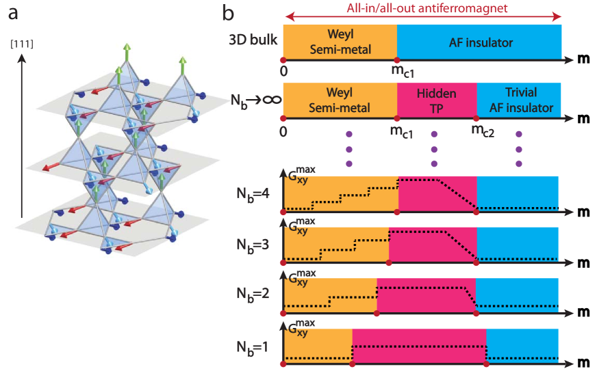
Considering recent advances in the study of Ir-based 5d TMOs, 19; 20 here we focus on the topological properties of pyrochlore iridate thin films. Since there are natural cleavage planes along the [111] or its symmetry equivalent directions, we investigate the dimensional crossover of [111] films varying the number of layers. The main results of this study are as follows. Most importantly, we find that the [111] thin film of pyrochlore iridates can show giant AHE. In particular, in the case of ultrathin films, the maximum magnitude of the anomalous Hall conductance is proportional to the total number of layers . In addition, we demonstrate the existence of a hidden topological phase between the Weyl-SM and the fully-gapped antiferromagnetic insulator (AFI) in thick films close to the bulk limit. Contrary to the common belief that Weyl-SM directly turns into a trivial AFI as the strength of the local Coulomb interaction () increases, we show that the topological properties of the Weyl-SM phase transfer to its neighboring fully gapped insulator for a finite range of values and bring about a new topological state in thin films. The nontrivial topological properties of the hidden topological phase are characterized by in-gap states localized on the surfaces and giant AHE. These results are summarized in the phase diagram of Fig. 2b.
Results
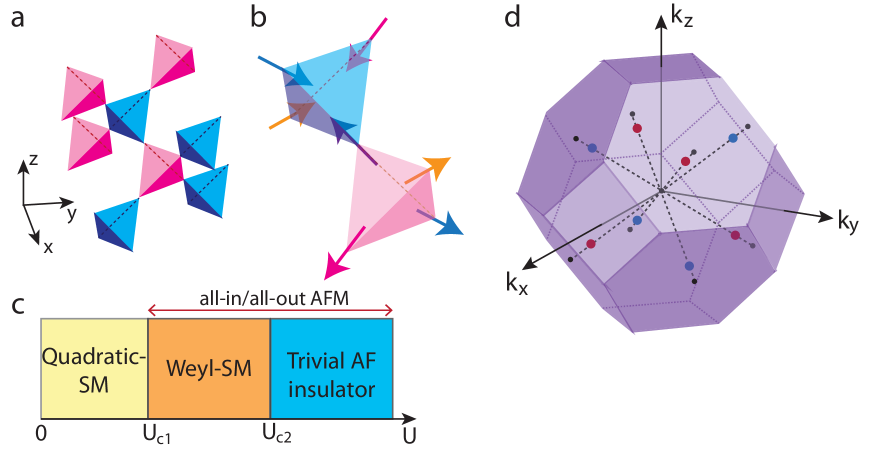
3D bulk properties. The pyrochlore lattice can be viewed as a face-centered cubic lattice with a tetrahedral unit cell as shown in Fig. 1a. In pyrochlore iridates, each Ir4+ ion sits on every corner of a tetrahedron. The candidate non-interacting ground states proposed up to now include a 3D topological insulator (TI) 21 and a semi-metal with quadratic band crossing at the Fermi level (quadratic-SM) 22; 23; 24 as well as conventional metallic states. 23 On the other hand, once electron-electron interactions are considered, an antiferromagnetic state with the all-in/all-out (AIAO) type local spin configuration can appear for according to the recent theoretical and experimental studies. 14; 23; 25; 27; 26 In the AIAO state, four spins residing on a tetrahedron always point to or away from the center of the tetrahedron as shown in Fig. 1b. The AIAO antiferromagnetic state supports two different types of ground states depending on , i.e., a Weyl-SM and a AFI as described in Fig. 1c. In fact, Weyl-SM phase has topological stability because each Weyl point (WP) carries an integer chiral charge. Therefore only when every WP is pair-annihilated by colliding with another WP with opposite chiral charge at , a gapped insulator can be obtained. In this way, the phase diagram of the 3D bulk system shows the continuous evolution from the non-magnetic ground state () to the Weyl-SM () and finally to the fully gapped AFI () as shown in Fig. 1c.
To describe the evolution of the ground state of the 3D bulk as well as the thin films consistently, we numerically study a lattice Hamiltonian whose detailed structure is shown in Methods section. To obtain the simple but realistic Hamiltonian capturing the key physical properties of pyrochlore iridates, it is assumed that the low energy physics of the system can be described by focusing on the doublet of Ir4+ with the effective total angular momentum , which is valid when the spin-orbit coupling is large enough. The transition from a nonmagnetic state to the antiferromagnetic state can be described by adding a local Hubbard-type interaction . According to the recent theoretical studies of the lattice Hamiltonian, 23; 25; 26 it is shown that when the quadratic-SM is the non-magnetic ground state, the local Coulomb interaction can give rise to the AIAO type magnetic ground state, consistent with the first-principle calculations and experiments. Considering the previous theoretical studies, we choose the parameters of the lattice Hamiltonian in a way that the quadratic-SM becomes the non-magnetic ground state of the system. Moreover, for the description of the local spin ordering pattern consistent with AIAO state, we introduce a vector at each lattice site , and use the magnitude of the local spin moment as a tunable parameter, representing the strength of . In this approach, the quadratic band touching point of the quadratic-SM locating at the point of the Brillouin zone (BZ) immediately splits into 8 WPs once . In this Weyl-SM phase, a pair of WPs are aligned along the [111] direction and the other 3 pairs of WPs are aligned along the other symmetry equivalent directions as shown in Fig. 1d. Moreover, the pair of WPs existing along the [111] direction have opposite chiral charges and the distance between them increases as increases. When , the pair reach a BZ boundary simultaneously and a pair-annihilation occurs. Because of the cubic symmetry, the same thing happens for the other 3 pairs of WPs leading to AFI. Therefore () is basically equivalent to the critical point at () in Fig. 1c.
Hall conductance of a Weyl-SM phase and cubic symmetry. The nontrivial physical response triggered by WPs is the intrinsic AHE. This is because a WP behaves like a fictitious magnetic monopole, which generates Berry gauge flux. Since the anomalous Hall conductivity is given by the integration of Berry gauge flux in the momentum space, Weyl-SM phase can show AHE. For example, the Hall conductivity of a Weyl-SM having only a pair of WPs at is given by , where is the distance between two WPs. 14; 28; 29 To understand the relation between the AHE and the distribution of WPs, it is convenient to introduce a Chern vector , which is defined as where is the fully-antisymmetric tensor with . 30; 28 Therefore, for a pair of WPs located at , the corresponding Chern vector would be and the location of the two Weyl points are at . As the distance between the two Weyl points increases, the Hall conductance of the system grows until the two Weyl points are pair-annihilated at the zone boundary. Once the pair-annihilation occurs, the system turns into an insulator with the quantized Hall conductivity of ( is the lattice constant along the -direction), which is nothing but the 3D Chern insulator (or the 3D quantum Hall insulator).
On the other hand, in the case of the Weyl-SM phase in pyrochlore iridates, there are 4 pairs of WPs due to the cubic symmetry of the system. Since a Chern vector can be assigned to each pair of WPs, there are in total four Chern vectors in the system. Note that correspond to the location of the WPs in the momentum space. However, since all WPs are related by the cubic symmetry, . Therefore the total Hall currents should be zero in the 3D bulk system. However, it should be stressed that although the net Chern vector of the system adds up to zero, the Weyl-SM phase of the pyrochlore iridates is still topologically nontrivial because there exist finite Chern vectors antiferromagnetically aligned, which are associated with the WPs. Once the cubic symmetry is broken, the incomplete cancelation of Chern vectors can generate nontrivial responses, which is the fundamental origin of emergent topological phenomena in thin films.
Moreover, we find that, surprisingly, even when all WPs are pair-annihilated and the system becomes an insulator, nontrivial topological responses still persist near the phase boundary between the Weyl-SM and the AFI as long as the cubic symmetry is broken. At the critical point () where all WPs hit the BZ boundary, the magnitude of each Chern vector reaches its maximum value. In contrast to the case of the system having only one Chern vector where the Chern vector with the maximum magnitude mediates the transition from a Weyl-SM to the 3D Chern insulator with the quantized Hall conductance, the antiferromagnetically aligned Chern vectors in pyrochlore iridates cannot support quantized topological number in the bulk insulator. However, once the cubic symmetry of the system is broken, for example, by making a thin film, the surface states associated with the antiferromagnetically aligned Chern vectors can induce nontrivial topological properties. For example, 2D conducting channels can appear on the surfaces or in the domain walls of the bulk insulator. Moreover, in the case of thin films having two parallel surfaces on the top and bottom layers, the coupling between two surface states can induce giant anomalous Hall conductance. Namely, the nontrivial topological property originating from the antiferromagnetically aligned Chern vectors, which is hidden in the 3D bulk insulator, can be manifested as the emerging topological properties of the thin films.
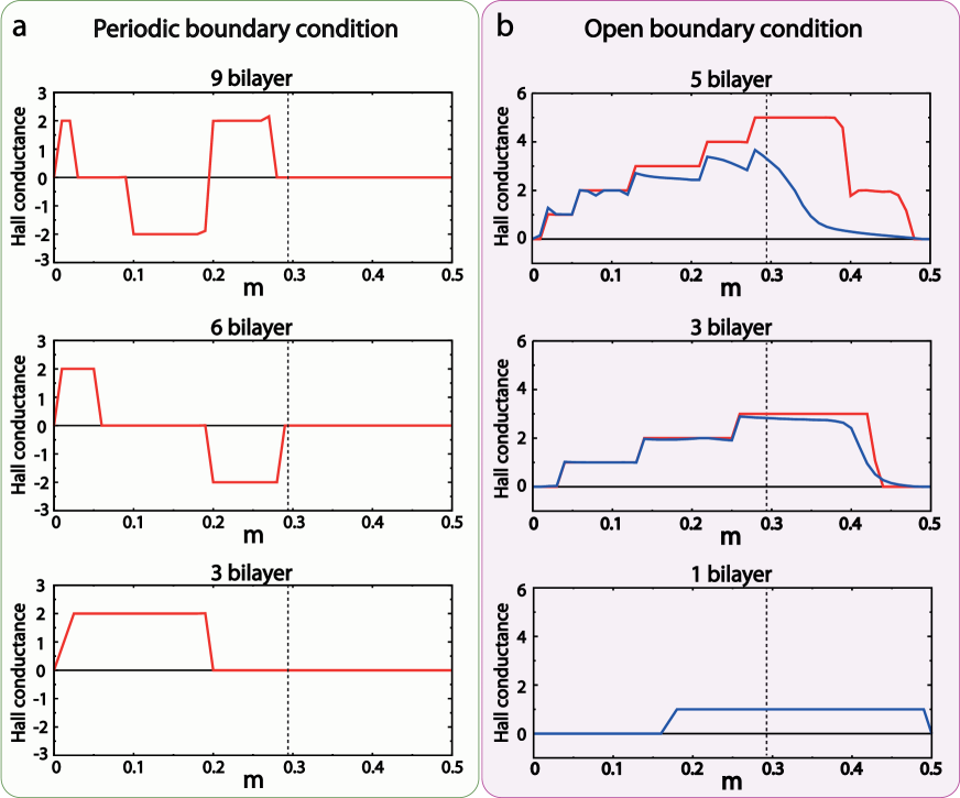
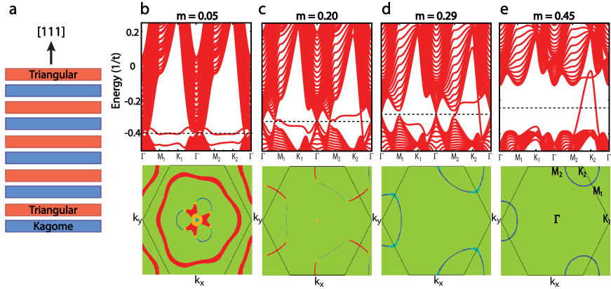
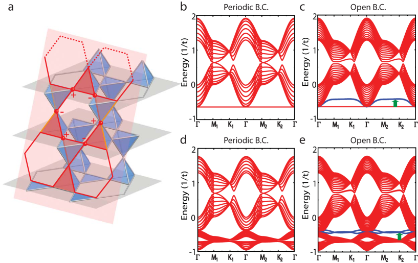
Topological properties of [111] thin films. An alternative way to view the pyrochlore lattice is that it is composed of alternating kagome and triangular lattices stacked along the [111] direction as shown in Fig. 2a. Because of such a peculiar lattice structure, the [111] plane provides a natural direction for film growth. Considering the tetrahedral unit cell, a bilayer composed of a pair of neighboring kagome and triangular lattices forms a basic building block for [111] films. In the following, we examine how the topological properties of thin films evolve as the number of bilayers () increases by computing the Hall conductance. Since the finite thickness of the film induces a small gap at the WPs, the bulk states do not touch the Fermi level for any in general, hence the Hall conductance is expected to be quantized. However, the nontrivial topological property of the bulk states supports surface states in the gap, which disturb the quantization of the Hall conductance in films. To understand the intrinsic topological property of thin films caused by the interplay between the bulk and surface states, we compute the Hall conductance of the system in two different ways. One way is to follow the conventional definition of the Hall conductance which is nothing but the integral of the Berry curvature of the occupied states below the Fermi energy. Because of the surface states in the gap, is normally not quantized if the film is not ultrathin (). In addition to , we define the maximum Hall conductance by imposing the half-filling condition at each momentum k locally and adding the contribution of locally half-filled bands over the entire Brillouin zone. Since the Fermi level can be in the gap locally in each k in this case, can be quantized.
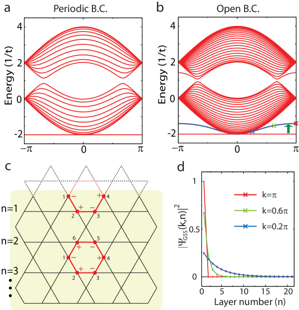
In Fig. 2b, we show the evolution of the phase diagram of films as varies. Surprisingly, Fig. 2b has unexpected rich structures. At first, when corresponding to the Weyl-SM phase in the bulk limit, the maximum Hall conductance ( is the length of the film) increases monotonously as increases, and eventually reaches the quantized value of near . This change is quite distinct from the oscillating predicted for films under the periodic boundary condition (BC) as shown in Figs. 3a, b. To understand such a strong BC dependence of , it is noted that the change of describes a topological phase transition induced by an accidental gap-closing. Therefore BC dependence of indicates the fact that gap-closing condition strongly depends on BC. In fact, a gapless WP of the bulk Weyl-SM phase turns into a gapped 2D Dirac point (GDP) in films due to the finite size effect. By changing , whenever an accidental gap-closing occurs at a GDP, shows a discontinuous change of . 31 Under the periodic BC, it can be shown that an accidental gap-closing can happen at each GDP separately by changing one external parameter that determines the location of bulk WPs. (See Methods.) Since the sign of varies depending on the location of WPs, the net contribution from all eight GDPs gives rise to the oscillating . On the other hand, under the open BC corresponding to the real situation of thin films, in general it is impossible to induce a gap-closing at a single GDP separately as shown in Methods section. In fact, under the open BC, the variation of an external parameter merely induces an overall shift of the energy spectrum near each GDP, hence the gap between the valence and conduction bands is fixed irrespective of the external parameter. However, even in this case, if the GDP has double degeneracy, gap-closing is possible. This is because when the energy spectrum of each of these two GDPs is shifted to the opposite direction, band touching can occur between the conduction band of one GDP and the valence band of the other GDP. (See Methods.) It is worth to note that in the case of [111] films, there always are one pair of WPs aligned along the -direction, which is a unique property of [111] films. Under the open BC, both of these WPs are projected to the center of the surface BZ while the other six WPs are projected to other six inequivalent points in the BZ. Therefore successive gap-closing is possible only at the point leading to monotonous stepwise increment of . In terms of Chern vectors, this means that among the four Chern vectors , only which is parallel to the -direction can contribute to . Since the maximum Hall conductance achievable through a pair of WPs related with is equal to , this limits the upper bound for of the film.
Contrary to the case of , the quantization of the physical Hall conductance is disturbed by the surface states in the bulk gap. As shown in Fig. 3b, the quantized can be observed only in ultrathin films with . However, the overall change of follows the variation of and a giant Hall conductance can be observed near the critical point . Moreover, it is worth to note that a finite Hall conductance always appears when . This clearly shows that there are two types of metallic conducting channels that can be observed even when the bulk material is insulating with . When there is a surface state touching the Fermi level in the gap, hence is not quantized as in the case of thick films, the top and bottom surfaces of the film support metallic states. On the other hand, when there is no state touching the Fermi level, hence is quantized as in the case of the ultrathin films, metallic conducting channels can appear at the domain wall due to the quantized Hall conductance.
The hidden topological property of the bulk insulator and emergent topological phenomena of the associated [111] thin films. The observation of the giant Hall conductance near the critical point at naturally leads to the following question: how does the system release such large Hall currents in the strong coupling limit where a topologically trivial Mott insulator is expected? Since the bulk states are fully gapped for , the release of Hall currents is possible only if the film supports intrinsic surface states which connect the bulk valence and conduction bands. The nontrivial topological property of the insulator, which is hidden in the 3D bulk system, manifests through the emergence of surface states carrying large Hall currents in thin films.
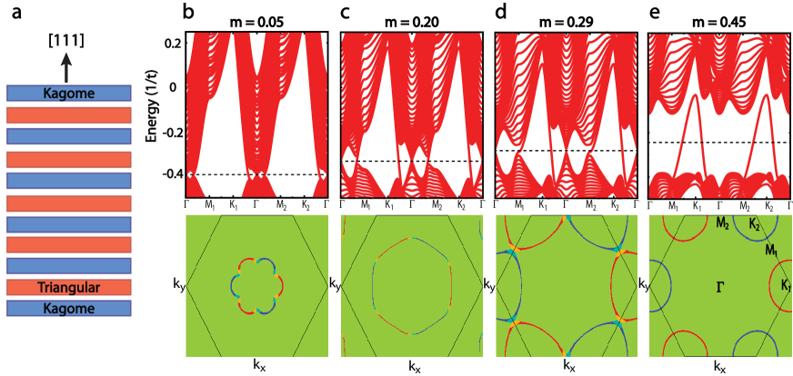
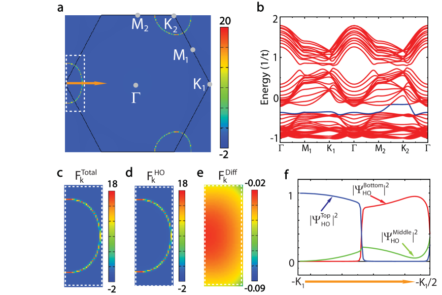
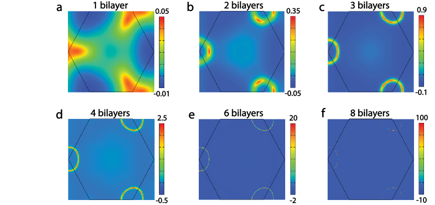
To understand the hidden topological property of the bulk insulator, let us first describe the band structure and surface spectrum of a [111] film with the thickness close to the bulk limit, which has the kagome lattice on both the top and bottom surfaces. As shown in Fig. 4, when , there are three pairs of Fermi arcs in the surface BZ whose end points correspond to the projected wave vectors of the bulk WPs to the surface. For , the total surface states, including the contribution from both the top and bottom surfaces, form a closed loop centered at the point and the size of the loop expands as increases as shown in Figs. 4b, c. However, at , the Fermi surface touches BZ boundary signaling a Lifshitz transition (Fig. 4d). Finally, when , the surface spectrum turns into two different closed loops centered at two corners of the BZ, respectively, as shown in Fig. 4e. It is worth to note that the surface spectrum does not immediately disappear even when and persists in the gap. In terms of the evolution of the surface spectrum, the critical point marks the point where the Fermi surface topology changes from the open Fermi surface (Fermi arcs) to the closed Fermi surfaces. Since the states localized on the top and bottom surfaces exist at different momenta, in general, there is no hybridization between these two surface states.
On the other hand, when the unit bilayers are stacked along the -direction, the top and bottom surfaces have different lattice structure. Let us assume that the top (bottom) surface has the triangular (kagome) lattice structure. One interesting property of the top surface terminated by a triangular lattice is that there are additional localized states which are not of topological origin. In fact, because of the lattice geometry, many localized states confined around each elementary hexagonal plaquette of the lattice can appear in the tight-binding Hamiltonian on the pyrochlore lattice. 32 When some of the hexagonal plaquettes near the surface are broken due to the lattice termination at the surface, the states, which were localized within those plaquettes before they are broken, are liberated from them and constitute a new surface state. (See Supplementary Note 1 and Supplementary Figure S1 and S2.) Such lattice geometry-induced surface states (geometrical-SS) can induce remarkable physical consequences. For example, as shown in Fig. 5e, even when , the conduction and valence bands are still coupled since there are two bands touching near the momentum . In fact, these two bands are surface states localized on the top and bottom surface layers, respectively. By comparing Fig. 4e and Fig. 5e, we can easily see that the surface states smoothly connected to the valence band are nothing but the surface states of topological origin related with the Weyl-SM phase (topological-SS). On the other hand, the other surface state connected to the conduction band is a geometrical-SS resulting from lattice geometry. Since these two surface states have different origins, they can appear at the same momentum, hence can be hybridized. Such a crossing between two surface states induces a huge change in and , finally leading to the trivial AFI at beyond which two surface states decouple. Since the giant Hall currents are released through the crossing of two surface states, the crossing points of two surface states should accompany pronounced Berry curvature distribution around them. As shown in Fig. 6 and Fig. 7, such a strong enhancement of the Berry curvature can be clearly observed near the region where two surface states are crossing.
Table 1 summarizes the topological properties of [111] thin films for various surface termination when the bulk is a fully gapped insulator with . The point is that the surface terminated by a triangular lattice has the topological-SS related with the Weyl-SM and the geometrical-SS related with the lattice structure at the same time. On the other hand, the surface terminated by a kagome lattice only has topological-SS. Notice that when the two surfaces have different lattice structures, the thin film can show the large anomalous Hall effect (AHE) when . As long as at least one surface of the film is terminated by the kagome lattice, 2D surface metallic states appear in the bulk gap. However, when the film has the triangular lattice on both surfaces, the topological-SS derived from Weyl-SM are destroyed by the geometrical-SS, hence the film becomes topologically trivial.
Discussion
As described above, the thin films of pyrochlore iridates offer a unique opportunity in many aspects. (i) This is the first realistic antiferromagnetic system showing the quantized AHE due to the scalar spin chirality without the uniform magnetization. 33 Namely, although the net magnetization vanishes due to the cancelation of four spin moments on each tetrahedron, the Chern numbers of Bloch states in momentum space remain nonzero and result in the quantized Hall conductance. The antiferromagnetic phase has two degenerate ground states, i.e., AIAO state and its time-reversed partner. Since the Hall conductances of these two phases have the opposite sign, metallic conducting channels can appear at domain walls as long as the domain wall plane is not perpendicular to the surface normal direction of the film. (ii) The bulk-surface correspondence in the thin films derived from the hidden topological phase belongs to a new class, i.e., the surface states carry large Chern numbers, which in principle can be proportional to the thickness of the film, while the 3D bulk system () is not topological and has a zero Chern number. This apparently contradicting behavior is explained by the fact that exponentially small overlap, i.e., ( is the correlation length determined by the transfer integral , the band gap and the lattice constant ), between the surface states on the top and bottom produces the Chern numbers, and hence carries the information about the bulk. In the limit of , this overlap can be neglected and the Chern number vanishes.
Now we remark on the relevant real materials. There are several antiferromagnets with AIAO spin structures such as Cd2Os2O7 and R2Ir2O7 (R=Nd, Sm, Eu). Furthermore, in these materials, one can control the strength of electron correlations. For example, the recent transport and optical studies on Nd2(Ir1-xRhx)2O7 have shown that insulator-metal transition can be achieved by replacing Ir by Rh. 34 Moreover, in this system, large additional conductivity is observed due to possible conducting channels at domain walls, not only when the bulk is expected to be a Weyl-SM state but also when it is a gapped insulator. 35 Our study clearly shows that the surface states associated with the anti-ferromagnetically aligned Chern vectors can appear when the bulk system is a gapped insulator as well as when it is a Weyl-SM, consistent with the experimental observation. Although the domain wall is different from the open surface in a strict sense, the emerging metallic states share the same topological origin. Such a metallic conduction at domain walls is also predicted in a recent theoretical study. 36
Finally, let us discuss about the influence of surface disorder in real materials. At first, when , the complexity of the surface is not crucial because the only requirement to observe the nontrivial change of Hall conductance induced by the topological charge of WP is to impose a sharp (hard wall) boundary condition, which is obviously achievable in experiments. However, disorder effect can be important when , especially related with the Hall conductance of the films. In contrast to the case of the films associated with the Weyl-SM phase where the change of Hall conductance is induced by bulk states, in the case of the films derived from the bulk insulator with , giant Hall currents are carried by two surface states whose wave function overlap is exponentially small in thick films. Therefore once the complexity of the surface is considered, the Hall currents of the films can be destroyed, especially, in the case of thick films. However, the quantized Hall conductance of ultrathin films having large hybridization gap between two surface states and the giant Hall response near the critical point can remain robustly even in the presence of disorder. Therefore although the interval between and can be reduced due to the disorder effect, the overall structure of the phase diagram should remain intact against disorder.
To conclude, we have theoretically studied the topological dimensional crossover phenomena in [111] thin films of pyrochlore iridates. We found the large anomalous Hall conductance even in the films associated with a fully gapped insulator in the bulk limit, which we call the hidden topological phase. The large Hall currents in the films derived from the bulk insulator phase is due to two surface states, i.e., one from the topological reason associated with WPs and the other from the geometrical reason of the lattice structure. Our theoretical study is based on the general tight-binding Hamiltonian, which captures the key intrinsic properties of pyrochlore iridates, hence can reproduce the essential physical properties of the 3D bulk system consistent with the first-principle calculations and experiments. Considering the growing experimental efforts to make 5d TMO thin films, it is expected that interesting experimental data on the pyrochlore iridate thin films would be available in near future, which would also provide useful guidance for more sophisticated numerical studies such as the first-principle calculations. This work will pave a way to explore the new emergent topological phenomena by artificial superstructures such as thin films in both theory and experiment.
Methods
Lattice Hamiltonian for pyrochlore iridates. To describe the evolution of the ground state for thin films as well as the 3D bulk system, we use the following lattice Hamiltonian proposed in Ref. 23;
| (1) |
where are Pauli matrices describing the effective spin degrees of freedom. Here it is assumed that the low energy physics of the system can be described by focusing on the doublet of Ir4+ with the effective total angular momentum , which is valid when the spin-orbit coupling is large enough. () indicates the hopping amplitude between the nearest-neighbor (next nearest neighbor) sites. The real vectors , , and describe dependent hopping terms. 23 The transition from a nonmagnetic state to the antiferromagnetic state can be described by adding , which can be considered as the result of a mean field approximation for the Hamiltonian with the Hubbard-type local interaction . 25 Here the vectors describe the local spin ordering patterns compatible with AIAO state.
Oscillating Hall conductance of [111] films in the Weyl-SM phase under the periodic BC. In Fig. 3a of the main text, we have shown the change of the Hall conductance (or Chern number) as increases under the periodic BC along the -direction, the surface normal direction of the film. When is within the range where the 3D bulk system is in a Weyl-SM phase, thin films show oscillating Hall conductance. Here we explain the origin of the oscillating in terms of Chern vectors. By definition, only the -component of each Chern vector can contribute to . In a [111] thin film, one of is parallel to the -direction. Suppose that is parallel to the -direction. Then the z-components of other Chern vectors is equal to . Since the sign of is opposite to that of , their contributions to also have the opposite sign. Let us first consider the contribution of to . Because of the finite-size effect, the momentum is discretized and only the discrete momenta within the range of can contribute to . On the other hand, in the case of , the discrete momenta within the range of can contribute to . Since the number of discrete momenta within the range of is not always equal to the triple of the number of discrete momenta within the range of , the oscillating appears. Notice that the maximum magnitude of the 3D conductivity vanishes in the bulk limit (), consistent with the constraint of in the bulk system. Such an oscillating is generally expected in the Weyl-SM phase with a zero total Chern vector, when the system has a thin film structure under the periodic boundary condition.
Accidental gap closing in thin films of the Weyl-SM phase. One peculiar property of the pyrochlore iridate [111] film is that the accidental gap-closing condition strongly depends on the boundary conditions. Namely, in the case of the periodic boundary condition, an accidental band crossing at a single Weyl point can be induced by changing the magnitude of the local spin moment (). On the other hand, under the open boundary condition, a gap-closing at a single Weyl point cannot be induced by controlling . Interestingly, in the case of the film with open boundary condition, only when a pair of Weyl points are aligned along the surface normal direction, band crossing occurs. Such a strong boundary condition dependence of the gap-closing condition gives rise to stark difference in the change of the Hall conductance of a film depending on the boundary conditions.
The origin of the boundary condition dependence of the gap-closing condition is as follows. At first, under the periodic boundary conditions, the typical eigenfunction and the corresponding eigenvalues of a Weyl fermion can be written as
where is the momentum component normal to the surface, , is the energy eigenvalue and is the velocity of the Weyl fermion. To determine the discrete value of the momentum , we consider the following periodic boundary condition, . It is worth to note that in general two wave functions at and can be different up to the overall U(1) phase . This is because when we derive the low energy Hamiltonian near the Weyl points, we assume where is the location of the Weyl point. Here is the full lattice eigenstate and is the low energy state near the Weyl point. Therefore if we impose , it is equivalent to . Since the location of the Weyl point depends on the local spin moment , we can obtain with . This condition immediately gives rise to discrete value with integer, and the corresponding energy eigenvalues given by
| (2) |
Here the point is that the relative energy eigenvalues depend only on one parameter . Therefore the accidental band crossing is possible when both and become zero simultaneously, i.e., . Since can take any integer value, successive gap closing is possible by tuning one parameter continuously.
On the other hand, the gap-closing condition under the open boundary condition is more complicated. After some straightforward calculation as shown in detail below, it can be shown that in general the energy eigenvalue of a single Weyl point can be written as
| (3) |
where is a constant. Note that the relative energy between and does not depend on . Therefore the variation of the parameter just induces the overall shift of the full energy spectrum and cannot induce band crossings at a single Weyl point. However, when two Weyl points are coupled, accidental band crossing is possible. For example, when a pair of Weyl points are along the surface normal direction, the open boundary condition induces mixing between these two Weyl points. Because of this mixing, the boundary condition induces a strong constraint to possible energy eigenvalues, which are given by
| (4) |
where , are constants. It is worth to note that while the energy levels for a Weyl point i.e., either or are shifted in parallel, the relative energy between and depends on one parameter . Since describes the overall shift of the energy, it can be absorbed to the chemical potential of the system, hence can be neglected. (Let .) Then, for example, if , ==0 is possible for any integer . Therefore successive gap-closing can be achieved by changing the parameter continuously.
Now let us describe the detailed derivation of the gap-closing condition under the open boundary condition. Here the idea is to understand how the energy spectrum near a Weyl point depends on hard wall boundary conditions. In general, a pair of Weyl fermions with opposite chiral charge can be described by
where the Pauli matrices describe two Weyl fermions and the velocity is assumed to be isotropic. Following McCann and Fal’ko, 37 we introduce a confinement potential at the boundary to describe a hard wall boundary condition for Weyl fermions in the following way,
| (5) |
where is a real constant and is an arbitrary 44 Hermitian, unitary matrix satisfying . We assume that is the surface normal direction of the hard wall and the wave function becomes zero outside the film. Then after integrating over a small region near the boundary, we obtain the following constraint.
| (6) |
From the equation above, it is straightforward to derive the following relations,
| (7) |
Therefore the boundary condition can be represented by the following local linear constraint to the wave function
| (8) |
in which satisfies
| (9) |
where . Here the anticommutation relation implies the absence of current along the surface normal direction. 38
The next step is to find the matrix satisfying Eq. (9). The most general form of can be written as
| (10) |
Using and imposing the constraints in Eq. (9), we can show that the most general form of is given by in which
| (11) |
and
| (12) |
where and . Here and the unit vectors and satisfy , . Therefore, in general, can be characterized by 4 independent parameters, , , , and another angular variable describing the orientation of or . Moreover, from the structure of , we can easily see that the Weyl fermion pair are coupled (decoupled) under (). Therefore when we describe the Weyl fermion pairs of a [111] film, which are not along the surface normal direction, since they are not coupled under the open boundary condition due to the translational invariance within the plane parallel to the surface, the boundary condition should be described by . On the other hand, when the pair of Weyl points are coupled under the boundary condition, in general, is possible. However, in the case of the Weyl fermion pair along [111] direction, additional rotational symmetry with respect to [111] direction (or ) can be imposed. Hence term is not allowed and should be satisfied.
Let us first discuss the case of decoupled Weyl fermion pairs with . If we assume that with , in Eq. (12) can be written as
| (13) |
Here () describes the top (bottom) surface at (). The wave function for two Weyl fermions can be written as where
and
The discrete value can be determined from the condition of at . Since we are interested in the gap-closing condition at the Weyl point, we can assume . Then using the discrete value, the corresponding energy eigenvalue () can be written as
| (14) |
for one Weyl fermion. Similarly, for the other Weyl fermion,
| (15) |
Here we can see that the energy eigenvalues explicitly depend on several parameters coming from the boundary condition. However, the energy spectrum is only globally shifted in each Weyl point and the relative energy between discrete eigenstates remains the same. It is to note that an accidental gap-closing is possible only when the energy gap between the conduction band and valence band can be tuned to zero. Therefore under the open boundary condition, two decoupled Weyl point cannot show an accidental gap closing.
Now let us consider the case of two coupled Weyl points. In this case the boundary condition can be imposed by using . The most general form of can be written as
| (16) |
which can be parametrized by two angular variables and . After repeating similar calculation, the energy spectrum at can be obtained as
| (17) |
and
| (18) |
Notice that contrary to the case of the decoupled Weyl points in Eq. (14)and Eq. (15), the relative energy between discrete energy eigenvalues depends on parameters resulting from the boundary condition. In this case, accidental band crossings can be achieved as explained in the beginning of this section.
References
- (1) Schnyder, A. P., Ryu, S., Furusaki, A., &Ludwig, A. W. W. Classification of Topological Insulators and Superconductors in Three Spatial Dimensions. Phys. Rev. B 78, 195125 (2008).
- (2) Schnyder, A. P., Ryu, S., Furusaki, A., &Ludwig, A. W. W. Classification of Topological Insulators and Superconductors. AIP Conf. Proc. 1134, 10 (2009).
- (3) Kitaev, A., Periodic Table for Topological Insulators and Superconductors. AIP Conf. Proc. 1134, 22 (2009).
- (4) Qi, X.- L., Hughes, T. L., & Zhang, S.- C., Topological Field Theory of Time-Reversal Invariant Insulators. Phys. Rev. B 78, 195424 (2008).
- (5) Haldane, F. D. M. Model for a Quantum Hall Effect without Landau Levels: Condensed-Matter Realization of the ”Parity Anomaly”. Phys. Rev. Lett. 61, 2015 (1988).
- (6) Kane, C. L. & Mele, E. J., Topological Order and the Quantum Spin Hall Effect. Phys. Rev. Lett. 95, 146802 (2005).
- (7) Kane, C. L. & Mele, E. J., Quantum Spin Hall Effect in Graphene. Phys. Rev. Lett. 95, 226801 (2005).
- (8) Fu, L., Kane, C. L. & Mele, E. J., Topological Insulators in Three Dimensions. Phys. Rev. Lett. 98, 106803 (2007).
- (9) Moore, J. E. & Balents, L. , Topological Invariants of Time-Reversal-Invariant Band Structures. Phys. Rev. B 75, 121306 (2007).
- (10) Roy, R., Topological Phases and the Quantum Spin Hall Effect in Threee Dimensions. Phys. Rev. B 79, 195322 (2009).
- (11) Essin, A. M.,Moore, J. E., & Vanderbilt, D., Magnetoelectri Polarizability and Axion Electrondynamics in Crystalline Insulators. Phys. Rev. Lett. 102, 146805 (2009).
- (12) Liu, C.- X., Zhang, H., Yan, B., Qi, X.- L.,Frauenheim, T.,Dai, X., Fang, Z., & Zhang, S.- C., Oscillatory Crossover from Two-Dimensional to Three-Dimensional Topological Insulators. Phys. Rev. B 81, 041307(R) (2010).
- (13) Xu, G.,Weng, H., Wang, Z.,Dai, X., & Fang, Z., Chern Semimetal and the Quantized Anomalous Hall Effect in HgCr2Se4. Phys. Rev. Lett. 107, 186806 (2011).
- (14) Wan, X., Turner, A. M., Vishwanath, A., & Savrasov, S. Y., Topological Semimetal and Fermi-Arc Surface States in the Electronic Structure of Pyrochlore Iridates. Phys. Rev. B 83, 205101 (2011).
- (15) Wan, X., Vishwanath, A., & Savrasov, S. Y., Computational Design of Axion Insulators Based on 5d Spinel Compounds. Phys. Rev. Lett. 108, 146601 (2012).
- (16) Turner, A. M., Zhang, Y.,Mong, R. S. K., & Vishwanath, A., Quantized Response and Topology of Magnetic Insulators with Inversion Symmetry. Phys. Rev. B 85, 165120 (2012).
- (17) Hwang, H. Y., Iwasa, Y., Kawasaki, M., Keimer, B., Nagaosa, N., & Tokura, Y., Emergent Phenomena at Oxide Interfaces. Nature Mater. 11, 103 (2012).
- (18) Xiao, D., Zhu, W.,Ran, Y.,Nagaosa, N., & Okamoto, S., Interface Enginnering of Quantum Hall Effects in Digital Transition Metal Oxide Heterostructure. Nature Comm. 2, 596 (2011).
- (19) Kim, B. J., Jin, H.,Moon, S. J., Kim, J. -Y.,Park, B. -G.,Leem, C. S., Yu, J.,Noh, T. W.,Kim, C., Oh, S. -J.,Park, J. -H.,Durairaj, V.,Cao, G., & Rotenberg, E., Novel Mott State Induced by Relativistic Spin-Orbit Coupling in Sr2IrO4. Phys. Rev. Lett. 101, 076402 (2008).
- (20) Kim, B. J., Ohsumi, H.,Komesu, T., Sakai, S.,Morita, T.,Takagi, H., & Arima, T., Phase Sensitive Observation of a Spin-Orbitial Mott State in Sr2IrO4. Science 323, 1329 (2009).
- (21) Pesin, D., & Balents, L., Mott Physics and Band Topology in Materials with Strong Spin-Orbit Interaction. Nature Phys. 6, 376 (2010).
- (22) Yang, B.- J., & Kim, Y. B., Topological Insulators and Metal-Insulator Transition in the Pyrochlore Iridates. Phys. Rev. B 82, 085111 (2010).
- (23) Witczak-Krempa, W.,Go, A., & Kim, Y. B., Pyrochlore Electrons under Pressure, Heat, and Field: Shedding Light on the Iridates. Phys. Rev. B 87, 155101 (2013).
- (24) Moon, E. -G.,Xu, C.,Kim, Y. B.,, & Balents, L., Non-Fermi-Liquid and Topological States with Strong Spin-Orbit Coupling. Phys. Rev. Lett. 111, 206401 (2013).
- (25) Witczak-Krempa, W., & Kim, Y. B., Topological and Magnetic Phases of Interacting Electrons in the Pyrochlore Iridates. Phys. Rev. B 85, 045124 (2012).
- (26) Go, A.,Witczak-Krempa, W.,Jeon, G. S., ,Park, K., & Kim, Y. B., Correlation Effects on 3D Topological Phases: from Bulk to Boundary. Phys. Rev. Lett 109, 066401 (2012).
- (27) Arima, T., Time-Reversal Symmetry Breaking and Consequent Physical Responses Induced by All-in/All-out Type Magnetic Order on the Pyrochlore Lattice. J. Phys. Soc. Jpn 82, 013705 (2013).
- (28) Yang, K. -Y.,Lu, Y. -M., & Ran, Y., Quantized Hall Effects in a Weyl Semimetal: Possible Application in Pyrochlore Iridates. Phys. Rev. B 84, 075129 (2011).
- (29) Burkov, A. A.& Balents, L., Weyl Semimetal in a Topological Insulator Multilayer. Phys. Rev. Lett 107, 127205 (2011).
- (30) Halperin, B. I., Possible States for a Three-Dimensional Electron Gas in a Strong Magnetic Field. Jpn. J. Appl. Phys. Suppl 26, 1913 (1987).
- (31) Oshikawa, M., Quantized Hall Conductivity of Bloch Electrons: Topology and the Dirac Fermion. Phys. Rev. B 50, 17357 (1994).
- (32) Bergman, D. L.,Wu, C., & Balents, L., Band Touching from Real-Space Topology in Frustrated Hopping Models. Phys. Rev. B 78, 125104 (2008).
- (33) Ohgushi, X., Murakami, S., & Nagaosa, N., Spin Anisotropy and Quantum Hall effect in the Kagome Lattice: Chiral Spin State Based on a Ferromagnet. Phys. Rev. B 62, R6065 (2000).
- (34) Ueda, K.,Fujioka, J.,Takahashi, Y., Suzuki, T.,Ishiwata, S.,Taguchi, Y., & Tokura, Y., Variation of Charge Dynamics in the Course of Metal-Insulator Transition for Pyrochlore Type Nd2Ir2O7. Phys. Rev. Lett 109, 136402 (2012).
- (35) Ueda, K., & Tokura, Y., Metallic Interface Emerging at Magnetic Domain Wall. Unpublished (2013).
- (36) Yamaji, Y., & Imada, M., Metallic Interface Emerging at Magnetic Domain Wall of Antiferromagnetic Insulator- Fate of Extinct Weyl Electrons. Preprint at http://arxiv.org/abs/1306.2022 (2013).
- (37) McCann, E. & Fal’ko, V. I., Symmetry of Boundary Conditions of the Dirac Equation for Electrons in Carbon Nanotubes.. J. Phys.: Condens. Matter 16, 2371–2379 (2004).
- (38) Akhmerov, A. R.& Beenakker, C. W. J., Boundary Conditions for Dirac Fermions on a Terminated Honeycomb Lattice. Phys. Rev. B 77, 085423 (2008).
Acknowledgements
We are grateful for support from the Japan Society for the Promotion of Science (JSPS) through the ‘Funding Program for World-Leading Innovative R&D on Science and Technology (FIRST Program). We thank David Vanderbilt for his insightful comments.
Supplementary Information
Localized states due to lattice geometry in the kagome lattice.
One peculiar property of [111] films is that there are additional non-topological surface states localized on the surface terminated by a triangular lattice. Here we will show that those additional localized states originate from the geometrical structure of the pyrochlore lattice.
Before we discuss about the localized states on the pyrochlore lattice, let us first consider the case of the kagome lattice which also supports non-topological localized states on the edge. The lattice structure of a kagome lattice is shown in Fig. 8c. To describe surface states we introduce a kagome ribbon indicated by the shaded region in Fig. 8c. A kagome ribbon has a sawtooth shape (a straight line shape) on the top (bottom) edge while the translational invariance is maintained along the horizontal direction (-direction). One simple way to make a kagome ribbon is vertical stacking of one-dimensional chains, each of which is composed of up-triangles connected along the -direction. Similar to the case of [111] films composed of stacked bilayers, the two edges of a kagome ribbon have asymmetric structures.
Now let us consider a tight-binding Hamiltonian describing hopping processes between nearest neighbor sites, which can be written as
| (19) |
where and are indices denoting the kagome lattice sites and indicates a nearest neighbor pair of sites. Fig. S1a shows the band structure of a kagome ribbon under the periodic boundary condition along the vertical direction. One interesting property of the band structure is that there are many flat bands at the energy . Such a flat band appears due to the localized state existing in a hexagonal plaquette. (See Ref. 32.) Explicitly, the wave function of the state localized in a hexagon can be written as
| (20) |
where (=1,…,6) indicates the six sites around a hexagon. Here indicates the vacuum state. An example of such a localized state in a hexagon is marked by red dots in Fig. 8c, in which indicates the sign in front of the state constituting . Since the number of hexagons is equal to the number of unit cells, a flat band can be formed by taking a linear superposition of every localized state in a hexagon. In fact, under the periodic boundary condition, localized hexagon states are under a constraint such that the summation of all localized hexagon states should vanish due to the absence of boundaries in a periodic system. However, since there are two additional degenerate localized states, which are so-called non-contractible loop states, a flat band can spread over the full Brillouin zone with additional band touching at the point. (See Ref. 32.)
Under the open boundary condition, the tight-binding Hamiltonian on a kagome ribbon shows an unexpected interesting feature. Fig. S1b describes the band structure of the system under the open boundary condition. Here we can see the appearance of an additional band, marked by a blue line in Fig. 8b, between the flat band and its neighboring dispersive band. By counting the number of flat bands at a fixed momentum, we can see that the additional blue band is a part of the flat band under the periodic boundary condition. Surprisingly, this additional band is exponentially localized near the sawtooth shaped edge of the strip as shown in Fig. 8d. The localization length of this additional state is inversely proportional to the energy gap between the flat band and its neighboring dispersive band at the given momentum. Let us call this localized state as a geometry-induced surface state (GSS). Considering the fact that the origin of the flat band is the localized state in a hexagon, we can easily find the origin of the GSS. As shown in Fig. 8c, at the sawtooth shaped edge, there are a series of broken hexagons aligned along the edge. It is to be noted that it is inevitable to create broken hexagons once a sawtooth shaped edge is introduced. The localized state related with a broken hexagon should be a part of flat bands under the periodic boundary condition. However, once a sawtooth shaped edge is introduced, the flat band which contains the localized states in hexagons touching the edge splits from the other flat bands, and forms the GSS.
To understand the relationship between the broken hexagon states and the GSS more explicitly, we can consider the following superposition of broken hexagon states,
| (21) |
where the index indicates a broken hexagon and () indicates the three sites in a corresponding broken hexagon. As can be seen in Fig. S1c, . The coefficients in front of and are fixed to find a state completely localized on the edge. After some straightforward calculations, it can be shown that the wave function of GSS at the momentum and can be written as
| (22) |
and
| (23) |
where are normalization constants. It means that the GSS is completely localized within broken hexagons at . As we move away from , shows small spreading along the vertical direction but is still exponentially localized near the sawtooth edge as shown in Fig. 8d. Since its localization length is determined by the gap between the flat band and its neighboring dispersive bulk bands, the GSS has stability. If additional hopping processes are considered, the localization length of the GSS can be changed due to the modified bulk band structure. However, as long as there is a finite gap at a given momentum, the GSS can be exponentially localized on the sawtooth edge.
In the case of , it is energetically degenerate with other flat bands coming from the localized states in hexagons. has nonzero amplitude only on site 2 and 3 in a broken hexagon and such a structure appears identically in every broken hexagon. In fact, is nothing but one of the non-contractible loop states, which extends along the -direction parallel to the sawtooth edge. In contrast to the case of 2D periodic systems where there are two non-contractible loop states, under the open BC there is only one non-contractible loop states since the geometry of the strip is basically a cylinder.
Localized states due to lattice geometry in [111] films. The additional localized states existing in [111] films can be understood by extending the idea of GSS in the kagome lattice to the pyrochlore lattice in a straightforward way. Pyrochlore lattice is composed of kagome planes which are stacked along or its three other symmetry equivalent directions. Let us first consider the tight-binding Hamiltonian containing only the nearest neighbor hopping amplitudes. Since each kagome plane supports localized states in each hexagon, the total number of localized states in hexagons is four times larger than the total number of unit cells in a pyrochlore lattice. However, those localized states in hexagons are not linearly independent. As discussed by Bergman et al. in Ref. 32 in the main text, if we consider a volume enclosed by four neighboring hexagons, the superposition of corresponding four localized states can be vanished. Taking into account of such local constraints, the total number of linearly independent localized states is almost two times larger than the number of unit cells, which is consistent with the fact that there are two completely flat bands in the bulk band structure as shown in Fig. 9b.
In the case of a [111] film, there are kagome planes stacked along the surface normal direction (-direction) of the film. Because of the translational invariance in planes, those kagome planes do not have broken hexagons. On the other hand, we also have to consider another group of parallel kagome planes to fully account for the flat bands in the bulk band structure. The surface normal direction of this second group of kagome planes is not parallel to the -direction. One example of such a slanted kagome plane is shown in Fig. 9a. Here the point is because of the structure of the film, each slanted kagome plane should have broken hexagons on the top surface of the film terminated by a triangular lattice plane. Such broken hexagons can generate GSS which is exponentially localized on the top surface of the film. To prove that the GSS results from the states in broken hexagons, we compute the energy spectrum of the film which has the triangular (kagome) lattice on the top (bottom) surface as shown in Fig. 9c. By comparing Fig. 9b and Fig. 9c, we can clearly see the emergence of the surface state (GSS) in a gap between the flat band and its neighboring dispersive bulk band, which is marked by a blue line in Fig. 9c. Also by counting the number of flat bands in both cases, we can see that the GSS is derived from the flat bands in Fig. 9b. Hence, the GSS is mainly from the states in broken hexagons on the top surface. Moreover, since the GSS is exponentially localized near the top surface and its localization length is given by the gap between the flat band and its neighboring dispersive bulk band, the GSS is stable against external perturbation as long as the gap remains finite. In Fig. 9d and Fig. 9e, we compare the band structure of the tight-binding Hamiltonian including the second nearest hopping and various effective spin dependent hopping processes. Due to the additional hopping processes, all bands are basically dispersive. But here we can still observe the existence of the GSS clearly. When the system possess another surface states such as the Fermi arc states of a Weyl-SM, the coupling between the Fermi arc states and the GSS can induce nontrivial topological phenomena driven by these surface states, which is the main topic discussed in the main text of the paper.
| Top Kagome Layer | Top Triangular Layer | |
| (Topological-SS only) | (Topological-SS + Geometrical-SS) | |
| Bottom Kagome Layer | No AHE | Giant AHE |
| (Topological-SS only) | (Metallic states in the gap) | (Metallic states in the gap) |
| Bottom Triangular Layer | Giant AHE | No AHE |
| (Topological-SS + Geometrical-SS) | (Metallic states in the gap) | (No metallic states in the gap) |
Table 1: Topological properties of [111] thin films for various surface termination when the bulk is a fully gapped insulator with .