Department of Physics, Harvard University, Cambridge, Massachusetts 02138, USA \alsoaffiliationSchool of Engineering and Applied Sciences, Harvard University, Cambridge, Massachusetts 02138, USA
Hole Spin Coherence in a Ge/Si Heterostructure Nanowire
Abstract
Relaxation and dephasing of hole spins are measured in a gate-defined Ge/Si nanowire double quantum dot using a fast pulsed-gate method and dispersive readout. An inhomogeneous dephasing time exceeds corresponding measurements in III-V semiconductors by more than an order of magnitude, as expected for predominately nuclear-spin-free materials. Dephasing is observed to be exponential in time, indicating the presence of a broadband noise source, rather than Gaussian, previously seen in systems with nuclear-spin-dominated dephasing.
Keywords: nanowire, spin qubit, dephasing, spin relaxation, dispersive readout
Competing financial interests: The authors declare no competing financial interests.
Realizing qubits that simultaneously provide long coherence times and fast control is a key challenge for quantum information processing. Spins in III-V semiconductor quantum dots can be electrically manipulated, but lose coherence due to interactions with nuclear spins 1, 2, 3. While dynamical decoupling and feedback have greatly improved coherence in III-V qubits 4, 5, 6, the simple approach of eliminating nuclear spins using group IV materials remains favorable. Carbon nanotubes have been investigated for this application 7, 8, 9, 10, but are difficult to work with due to uncontrolled, chirality-dependent electronic properties. So far, coherence has not been improved over III-V spin qubits.
Si devices have shown improved coherence for gate-defined electron quantum dots 11, 12, 13, 14, and for electron and nuclear spins of phosphorous donors 15, 16, 17, 18. The Ge/Si core/shell heterostructured nanowire is an example of a predominantly zero-nuclear-spin system that is particularly tunable and scalable 19, 20, 21, 22, 23. Holes in Ge/Si nanowires exhibit large spin-orbit coupling 24, 25, 26, a useful resource for fast, all-electrical control of single spins 27, 28, 29, 30, 10. Moving to holes should also improve coherence because the contact hyperfine interaction, though strong for electrons associated with -orbitals, is absent for holes associated with -orbitals 31. Indeed, a suppression of electron-nuclear coupling in hole conductors was recently demonstrated in InSb 32.
Here, we measure spin coherence times of gate-confined hole spins in a Ge/Si nanowire double quantum dot using high bandwidth electrical control and read out of the spin state. We find inhomogeneous dephasing times up to , twenty times longer than in III-V semiconductors. This timescale is consistent with dephasing due to sparse 73Ge nuclear spins. The observed exponential coherence decay suggests a dephasing source with high-frequency spectral content, and we discuss a few candidate mechanisms. These results pave the way towards improved spin-orbit qubits and strong spin-cavity coupling in circuit quantum electrodynamics 33.
Ge/Si core/shell nanowires host a tunable hole gas in the Ge core [Fig. 1(a)] with typical mobility . In the presence of realistic external electric fields, the 1D hole gas is expected to occupy a single Rashba-split subband with spin-orbit splitting, based on theory 25 and previous experiments 24, 26. Fabrication of double dots with discrete hole states, and measurements of spin relaxation have been reported 34, 35.
The device, diagrammed in Fig. 1(b), is fabricated on a lightly doped Si substrate. The substrate, insulating at , is covered with using atomic layer deposition. Nanowires are deposited from methanol solution and contacted by evaporating Al following a buffered hydrofluoric acid dip. A second layer of covers the wire, and Cr/Au electrostatic gates are placed on top. These gates tune the hole density along the length of the wire. All data are obtained at temperature in a dilution refrigerator with external magnetic field , unless otherwise noted.
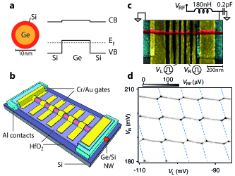
Gate voltages are tuned to form a double quantum dot in the nanowire with control over charge occupancy and tunnel rates. High-bandwidth () plunger gates and , labeled in Fig. 1(c), control hole occupation in the left and right dots. The readout circuit is formed by wire bonding a 180 nH inductor directly to the source electrode of the device. Combined with a total parasitic capacitance of , this forms an LC resonance at with bandwidth . Tunneling of holes between dots or between the right dot and lead results in a capacitive load on the readout circuit, shifting its resonant frequency. 36, 37. The circuit response is monitored by applying near-resonant excitation to the readout circuit and recording changes in the reflected voltage, , after amplification at and demodulation using a power splitter and two mixers at room temperature \bibnote S. Weinreb LNA SN68. Minicircuits ZP-2MH mixers. Tektronix AWG5014 waveform generator used on and . Coilcraft 0603CS chip inductor..
The charge stability diagram of the double dot is measured by monitoring at fixed frequency while slowly sweeping and [Fig. 1(d)]. Lines are observed whenever single holes are transferred to or from the right dot. Transitions between the left dot and left lead are below the noise floor (not visible) because the LC circuit is attached to the right lead. Enhanced signal is observed at the triple points, where tunneling is energetically allowed across the entire device. The observed “honeycomb” pattern is consistent with that of a capacitively-coupled double quantum dot 39. The charging energies for the left and right dots are estimated and from Fig. 1(d), using a plunger lever arm of eV/V, determined from finite bias measurements on similar devices 34. The few-hole regime was accessible only in the right dot, identified by an increase in charging energy. Based on the location of the few-hole regime in the right dot, we estimate the left and right hole occupations to be 70 and 10 at the studied tuning. We found that operating in the many-hole regime improved device stability, facilitating gate tuning and readout. We do not know if this affects the quality of the qubit, as recently found for electron spins in GaAs 40.
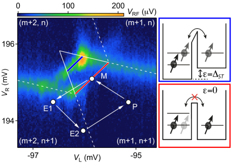
The spin state of the double dot is read out by mapping it onto a charge state using the Pauli blockade pulse sequence diagrammed in Fig. 2. At the points E1 and E2 (“empty”) the double dot is in the (m+2, n+1) charge state, assuming that m (n) paired holes occupy lower orbitals in the left (right) dot. Pulsing to P (“prepare”) in (m+1, n+1) discards one hole from the left dot, leaving the spin state of the double dot in a random mixture of singlet and triplet states. Moving to M (“measure”) adjusts the energy detuning between the dots, making interdot tunneling favorable. When M is located at zero detuning, , tunneling is allowed for singlet but Pauli-blocked for triplet states. When M is at the singlet-triplet splitting, , triplet states can tunnel. The location of the interdot charge transition therefore reads out the spin state of the double dot. We expect this picture to be valid for multi-hole dots with an effective spin- ground state 35, 41, 42, 40. We use singlet-triplet terminology for clarity, but note that strong spin-orbit coupling changes the spin makeup of the blockaded states without destroying Pauli blockade 43.
The fast pulse sequence is repeated continuously while rastering the position of near the (m+1, n+1)-(m+2, n) charge transition (Fig. 2). The RF carrier is applied only at the measurement point, M. As shown in Fig. 1(d), features with negative slope are observed corresponding to transitions across the right barrier. We interpret the weak interdot transition at zero detuning accompanied by a relatively strong interdot feature at large detuning as Pauli blockade of the ground-state interdot transition (), and lifting of blockade at the singlet-triplet splitting (). The strength of the interdot transition thus measures the probability of loading a singlet at point P, while the strength at measures the probability of loading a triplet. As a control, the Pauli blockade pulse sequence was run in the opposite direction, and no blockade was observed (see Supporting Information).
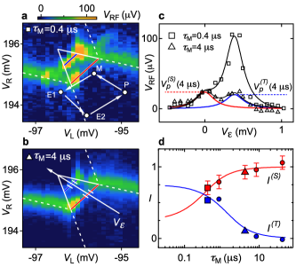
Spin relaxation is measured by varying the dwell time at the measurement point for the counterclockwise Pauli-blockade sequence. As increases the triplet transition weakens and the singlet transition strengthens [Fig. 3(a,b)] due to triplet-to-singlet spin relaxation. Note that these relaxation processes have different charge characters at different measurement points. For example, at the initial charge state is (m+1, n+1), whereas at the initial charge state is hybridized with (m+2, n).
The spin relaxation time is measured by analyzing a cut along the axis [shown in Fig. 3(b)] and varying . For each , the cut is fit to the sum of two Lorentzians with equal widths and constant spacing. The heights are for the triplet peak and for the singlet peak. Two example cuts are shown in Fig. 3(c), along with fits to exponential forms,
| (1) | |||||
| (2) |
where is the exponential decay averaged over the measurement time. Figure 3(d) plots the readout visibility, . The extracted relaxation time is at the triplet position [blue line in Figs. 3(a,b)], and at the singlet position [red line in Figs. 3(a,b)]. We note that these spin relaxation times are three orders of magnitude shorter than those previously measured in a similar device in a more isolated gate configuration and away from interdot transitions 35. Detuning dependence of spin relaxation has been observed previously and attributed to detuning-dependent coupling to the leads as well as hyperfine effects (presumably the former dominate here) 44, 45. Relaxation due to the spin-orbit interaction is expected to take microseconds or longer 46. The difference between and can possibly be attributed to differences in singlet-singlet and triplet-triplet tunnel couplings or enhanced coupling near the edges of the pulse triangle. The separation between Lorentzian peaks by can be interpreted as , using a plunger lever arms of eV/V.

To investigate spin dephasing, an alternate pulse sequence is used that first initializes the system into a singlet state in (m+2, n) at point P, then separates to point S (“separate”) in (m+1, n+1) for a time [Fig. 4(a)]. The spin state of the double dot is measured at M by pulsing back towards (m+2, n). For short [Fig. 4(a)] a strong singlet return feature is observed, consistent with negligible spin dephasing. For long [Fig. 4(b)], a strong triplet return feature is observed, consistent with complete spin dephasing.
The dephasing time is found by measuring at the triplet transition, and plotting the normalized differential voltage as a function of separation time [Fig. 4(c)]. Here, is the demodulated voltage for a pulse sequence with long dephasing time. The quantity is directly measured by alternating between the sequence and a reference sequence with long dephasing time, and feeding the demodulated voltage into a lock-in amplifier. Fitting the data to yields . Figure 4(c) shows exponential fits () for both data sets. The data decays exponentially on a timescale . Data acquired at at a different double-dot occupation give a similar timescale and functional form.
Although this timescale is approaching the limit expected for dephasing due to random Zeeman gradients from sparse 73Ge nuclear spins (see Supporting Information), the observed exponential loss of coherence is by and large unexpected for nuclei. A low-frequency-dominated nuclear bath is expected to yield a Gaussian fall-off of coherence with time 47, in contrast to the observed exponential dependence, which instead indicates a rapidly varying bath 48. Nuclei can produce high-bandwidth noise in the presence of spatially varying effective magnetic fields, for example due to inhomogeneous strain-induced quadrupolar interactions 49. The similarity of data at and T in Fig. 4(c), however, would indicate an unusually large energy-scale for nuclear effects. Electrical noise, most likely from the sample itself, combined with spin-orbit coupling is a plausible alternative. For electrons, the ubiquitous electrical noise alone does not result in pure dephasing 50, but can add high-frequency noise to the low-frequency contribution from the nuclear bath. It is conceivable that the behavior is different for holes, but this has not been studied to our knowledge. The relative importance of nuclei versus electrical noise could be quantified in future experiments by studying spin coherence in isotopically pure Ge/Si nanowires.
Cuts along the axis in Fig. 4(b) as a function of provide a second method for obtaining , following analysis along the lines of Fig. 3(c). The resulting probability versus is shown in Fig. 4(d), along with exponential curves
| (3) | |||||
| (4) |
using , with and as fit parameters. Depending on the nature of the dephasing, the singlet probability settling value, , is expected to range from for quasi-static Zeeman gradients to for rapidly varying baths 51, 52, 53. We find . Equations (3,4) do not take into account spin relaxation at the measurement point, meaning that the fitted systematically overestimates the true settling value \bibnoteWe do not correct for effects in Eqs. (3,4), as differed significantly from those observed in Fig. 3.. Therefore, we conclude that the data weakly support rather than , consistent with our inference of a rapidly varying bath.
Unexplained high-frequency noise has recently been observed in other strong spin-orbit systems, such as InAs nanowires 28, InSb nanowires 30, and carbon nanotubes 10. In these systems slowly varying nuclear effects were removed using dynamical decoupling, revealing the presence of unexplained high-frequency noise. In our system the effect of nuclei is reduced by the choice of material, and an unexplained high-frequency noise source appears directly in the . These similarities suggest the existence of a shared dephasing mechanism that involves spin-orbit coupling.
Future qubits based on Ge/Si wires could be coupled capacitively 55, 56 or through a cavity using circuit quantum electrodynamics 33, 45. In the latter case, the long dephasing times measured here suggest that the strong coupling regime may be accessible.
We acknowledge helpful discussions with Félix Beaudoin, William Coish, Jeroen Danon, Xuedong Hu, Christoph Kloeffel, Daniel Loss, Franziska Maier and Mark Rudner, and experimental assistance from Patrick Herring. Funding from the Department of Energy, Office of Science & SCGF, the EC FP7-ICT project SiSPIN № 323841, and the Danish National Research Foundation is acknowledged.
Supporting information is provided on acquisition method for Figure 1d, image analysis methods, clockwise pulse sequence (control experiment), and theoretical estimate of timescale for Ge/Si nanowire.
References
- Petta et al. 2005 Petta, J. R.; Johnson, A. C.; Taylor, J. M.; Laird, E. A.; Yacoby, A.; Lukin, M. D.; Marcus, C. M.; Hanson, M. P.; Gossard, A. C. Science 2005, 309, 2180–2184
- Koppens et al. 2006 Koppens, F.; Buizert, C.; Tielrooij, K.-J.; Vink, I. T.; Nowack, K. C.; Meunier, T.; Kouwenhoven, L. P.; Vandersypen, L. Nature 2006, 442, 766–771
- Hanson et al. 2007 Hanson, R.; Kouwenhoven, L. P.; Petta, J. R.; Tarucha, S.; Vandersypen, L. M. K. Rev. Mod. Phys. 2007, 79, 1217
- Bluhm et al. 2011 Bluhm, H.; Foletti, S.; Neder, I.; Rudner, M.; Mahalu, D.; Umansky, V.; Yacoby, A. Nat. Phys. 2011, 7, 109–113
- Medford et al. 2012 Medford, J.; Cywiński, Ł.; Barthel, C.; Marcus, C. M.; Hanson, M. P.; Gossard, A. C. Phys. Rev. Lett. 2012, 108, 086802
- Bluhm et al. 2010 Bluhm, H.; Foletti, S.; Mahalu, D.; Umansky, V.; Yacoby, A. Phys. Rev. Lett. 2010, 105, 216803
- Churchill et al. 2009 Churchill, H. O. H.; Kuemmeth, F.; Harlow, J. W.; Bestwick, A. J.; Rashba, E. I.; Flensberg, K.; Stwertka, C. H.; Taychatanapat, T.; Watson, S. K.; Marcus, C. M. Phys. Rev. Lett. 2009, 102, 166802
- Churchill et al. 2009 Churchill, H. O. H.; Bestwick, A. J.; Harlow, J. W.; Kuemmeth, F.; Marcos, D.; Stwertka, C. H.; Watson, S. K.; Marcus, C. M. Nat. Phys. 2009, 5, 321–326
- Pei et al. 2012 Pei, F.; Laird, E. A.; Steele, G. A.; Kouwenhoven, L. P. Nat. Nanotechnol. 2012, 7, 630–634
- Laird et al. 2013 Laird, E. A.; Pei, F.; Kouwenhoven, L. P. Nat. Nanotechnol. 2013, 8, 565–568
- Goswami et al. 2007 Goswami, S.; Slinker, K. A.; Friesen, M.; McGuire, L. M.; Truitt, J. L.; Tahan, C.; Klein, L. J.; Chu, J. O.; Mooney, P. M.; van der Weide, D. W.; Joynt, R.; Coppersmith, S. N.; Eriksson, M. A. Nat. Phys. 2007, 3, 41–45
- Shaji et al. 2008 Shaji, N.; Simmons, C. B.; Thalakulam, M.; Klein, L. J.; Qin, H.; Luo, H.; Savage, D. E.; Lagally, M. G.; Rimberg, A. J.; Joynt, R.; Friesen, M.; Blick, R. H.; Coppersmith, S. N.; Eriksson, M. A. Nat. Phys. 2008, 4, 540–544
- Maune et al. 2012 Maune, B. M.; Borselli, M. G.; Huang, B.; Ladd, T. D.; Deelman, P. W.; Holabird, K. S.; Kiselev, A. A.; Alvarado-Rodriguez, I.; Ross, R. S.; Schmitz, A. E.; Sokolich, M.; Watson, C. A.; Gyure, M. F.; Hunter, A. T. Nature 2012, 481, 344–347
- Shi et al. 2014 Shi, Z.; Simmons, C. B.; Ward, D. R.; Prance, J. R.; Wu, X.; Koh, T. S.; Gamble, J. K.; Savage, D. E.; Lagally, M. G.; Friesen, M. Nat. Commun. 2014, 5, 3020
- Pla et al. 2012 Pla, J. J.; Tan, K. Y.; Dehollain, J. P.; Lim, W. H.; Morton, J. J. L.; Jamieson, D. N.; Dzurak, A. S.; Morello, A. Nature 2012, 489, 541–545
- Pla et al. 2013 Pla, J. J.; Tan, K. Y.; Dehollain, J. P.; Lim, W. H.; Morton, J. J. L.; Zwanenburg, F. A.; Jamieson, D. N.; Dzurak, A. S.; Morello, A. Nature 2013, 496, 334–338
- Dehollain et al. 2014 Dehollain, J. P.; Muhonen, J. T.; Tan, K. Y.; Jamieson, D. N.; Dzurak, A. S.; Morello, A. arXiv.org 2014, 1402.7148v1
- Muhonen et al. 2014 Muhonen, J. T.; Dehollain, J. P.; Laucht, A.; Hudson, F. E.; Sekiguchi, T.; Itoh, K. M.; Jamieson, D. N.; McCallum, J. C.; Dzurak, A. S.; Morello, A. arXiv.org 2014, 1402.7140v1
- Lu et al. 2005 Lu, W.; Xiang, J.; Timko, B. P.; Wu, Y.; Lieber, C. M. Proc. Natl. Acad. Sci. U. S. A. 2005, 102, 10046–10051
- Xiang et al. 2006 Xiang, J.; Lu, W.; Hu, Y.; Wu, Y.; Yan, H.; Lieber, C. M. Nature 2006, 441, 489–493
- Yan et al. 2011 Yan, H.; Choe, H. S.; Nam, S.; Hu, Y.; Das, S.; Klemic, J. F.; Ellenbogen, J. C.; Lieber, C. M. Nature 2011, 470, 240–244
- Yao et al. 2013 Yao, J.; Yan, H.; Lieber, C. M. Nat. Nanotechnol. 2013, 8, 329–335
- Yao et al. 2014 Yao, J.; Yan, H.; Das, S.; Klemic, J. F.; Ellenbogen, J. C.; Lieber, C. M. Proc. Natl. Acad. Sci. U. S. A. 2014, 111, 2431–2435
- Hao et al. 2010 Hao, X.-J.; Tu, T.; Cao, G.; Zhou, C.; Li, H.-O.; Guo, G.-C.; Fung, W. Y.; Ji, Z.; Guo, G.-P.; Lu, W. Nano Lett. 2010, 10, 2956–2960
- Kloeffel et al. 2011 Kloeffel, C.; Trif, M.; Loss, D. Phys. Rev. B 2011, 84, 195314
- Higginbotham et al. 2014 Higginbotham, A. P.; Kuemmeth, F.; Larsen, T. W.; Fitzpatrick, M.; Yao, J.; Yan, H.; Lieber, C. M.; Marcus, C. M. arXiv.org 2014, 1401.2948v1
- Nowack et al. 2007 Nowack, K. C.; Koppens, F. H. L.; Nazarov, Y. V.; Vandersypen, L. M. K. Science 2007, 318, 1430–1433
- Nadj-Perge et al. 2010 Nadj-Perge, S.; Frolov, S. M.; Bakkers, E. P. A. M.; Kouwenhoven, L. P. Nature 2010, 468, 1084–1087
- Nowack et al. 2011 Nowack, K. C.; Shafiei, M.; Laforest, M.; Prawiroatmodjo, G. E. D. K.; Schreiber, L. R.; Reichl, C.; Wegscheider, W.; Vandersypen, L. M. K. Science 2011, 333, 1269–1272
- van den Berg et al. 2013 van den Berg, J. W. G.; Nadj-Perge, S.; Pribiag, V. S.; Plissard, S. R.; Bakkers, E. P. A. M.; Frolov, S. M.; Kouwenhoven, L. P. Phys. Rev. Lett. 2013, 110, 066806
- Fischer et al. 2008 Fischer, J.; Coish, W. A.; Bulaev, D. V.; Loss, D. Phys. Rev. B 2008, 78, 155329
- Pribiag et al. 2013 Pribiag, V. S.; Nadj-Perge, S.; Frolov, S. M.; van den Berg, J. W. G.; van Weperen, I.; Plissard, S. R.; Bakkers, E. P. A. M.; Kouwenhoven, L. P. Nat. Nanotechnol. 2013, 8, 170–174
- Kloeffel et al. 2013 Kloeffel, C.; Trif, M.; Stano, P.; Loss, D. Phys. Rev. B 2013, 88, 241405
- Hu et al. 2007 Hu, Y.; Churchill, H. O. H.; Reilly, D. J.; Xiang, J.; Lieber, C. M.; Marcus, C. M. Nat. Nanotechnol. 2007, 2, 622–625
- Hu et al. 2012 Hu, Y.; Kuemmeth, F.; Lieber, C. M.; Marcus, C. M. Nat. Nanotechnol. 2012, 7, 47–50
- Petersson et al. 2010 Petersson, K. D.; Smith, C. G.; Anderson, D.; Atkinson, P.; Jones, G.; Ritchie, D. A. Nano Lett. 2010, 10, 2789–2793
- Jung et al. 2012 Jung, M.; Schroer, M. D.; Petersson, K. D.; Petta, J. R. Appl. Phys. Lett. 2012, 100, 253508
- 38 S. Weinreb LNA SN68. Minicircuits ZP-2MH mixers. Tektronix AWG5014 waveform generator used on and . Coilcraft 0603CS chip inductor.
- van der Wiel et al. 2002 van der Wiel, W.; De Franceschi, S.; Elzerman, J.; Fujisawa, T.; Tarucha, S.; Kouwenhoven, L. Rev. Mod. Phys. 2002, 75, 1–22
- Higginbotham et al. 2014 Higginbotham, A. P.; Kuemmeth, F.; Hanson, M. P.; Gossard, A. C.; Marcus, C. M. Phys. Rev. Lett. 2014, 112, 026801
- Vorojtsov et al. 2004 Vorojtsov, S.; Mucciolo, E. R.; Baranger, H. U. Phys. Rev. B 2004, 69, 115329
- Johnson et al. 2005 Johnson, A. C.; Petta, J. R.; Marcus, C. M.; Hanson, M. P.; Gossard, A. C. Phys. Rev. B 2005, 72, 165308
- Danon and Nazarov 2009 Danon, J.; Nazarov, Y. V. Phys. Rev. B 2009, 80, 041301
- Johnson et al. 2005 Johnson, A. C.; Petta, J. R.; Taylor, J. M.; Yacoby, A.; Lukin, M. D.; Marcus, C. M.; Hanson, M. P.; Gossard, A. C. Nature 2005, 435, 925–928
- Petersson et al. 2012 Petersson, K. D.; McFaul, L. W.; Schroer, M. D.; Jung, M.; Taylor, J. M.; Houck, A. A.; Petta, J. R. Nature 2012, 490, 380–383
- Maier et al. 2013 Maier, F.; Kloeffel, C.; Loss, D. Phys. Rev. B 2013, 87, 161305
- Coish and Loss 2005 Coish, W. A.; Loss, D. Phys. Rev. B 2005, 72, 125337
- Cywiński et al. 2008 Cywiński, Ł.; Lutchyn, R.; Nave, C.; Das Sarma, S. Phys. Rev. B 2008, 77, 174509
- Beaudoin and Coish 2013 Beaudoin, F.; Coish, W. A. Phys. Rev. B 2013, 88, 085320
- Huang and Hu 2013 Huang, P.; Hu, X. arXiv.org 2013, 1308.0352v2
- Schulten and Wolynes 1978 Schulten, K.; Wolynes, P. G. J. Chem. Phys. 1978, 68, 3292–3297
- Merkulov et al. 2002 Merkulov, I. A.; Efros, A. L.; Rosen, M. Phys. Rev. B 2002, 65, 205309
- Zhang et al. 2006 Zhang, W.; Dobrovitski, V. V.; Al-Hassanieh, K. A.; Dagotto, E.; Harmon, B. N. Phys. Rev. B 2006, 74, 205313
- 54 We do not correct for effects in Eqs. (3,4), as differed significantly from those observed in Fig. 3.
- Trifunovic et al. 2012 Trifunovic, L.; Dial, O.; Trif, M.; Wootton, J. R.; Abebe, R.; Yacoby, A.; Loss, D. Phys. Rev. X 2012, 2, 011006
- Shulman et al. 2012 Shulman, M. D.; Dial, O. E.; Harvey, S. P.; Bluhm, H.; Umansky, V.; Yacoby, A. Science 2012, 336, 202–205