Phys. Rev. Lett. (2014)
Semiconducting layered blue phosphorus:
A computational study
Abstract
We investigate a previously unknown phase of phosphorus that shares its layered structure and high stability with the black phosphorus allotrope. We find the in-plane hexagonal structure and bulk layer stacking of this structure, which we call ‘blue phosphorus’, to be related to graphite. Unlike graphite and black phosphorus, blue phosphorus displays a wide fundamental band gap. Still, it should exfoliate easily to form quasi-2D structures suitable for electronic applications. We study a likely transformation pathway from black to blue phosphorus and discuss possible ways to synthesize the new structure.
pacs:
73.20.At, 73.61.Cw, 61.46.-w, 73.22.-fElemental phosphorus is stable in a large number of structures, including the common white, red, violet and black allotropesHultgren et al. (1935); Thurn and Kerbs (1966), with the color defined by the fundamental band gap. Most stable among them is black phosphorus, which – besides graphitic carbon – is the only layered structure of an elemental solid we know of. Individual layers of black phosphorus, shown in Fig. 1(a), resemble the honeycomb structure of graphene in terms of connectivity, but are non-planar. We noted that specific dislocations may convert black phosphorus, characterized by armchair ridges in the side view of the layers, to a well-defined structure with zigzag puckering, shown in Fig. 1(b). Assuming that the modified structure is stable, it appears worthwhile to study the equilibrium atomic arrangement in the bulk and the possibility of exfoliating individual layers. Whereas the observed fundamental band gap of 0.3-0.4 eV in black phosphorusMaruyama et al. (1981); Narita et al. (1983) is rather narrow, it is intriguing to see if the modified phosphorus structure is a semiconductor with a wider gap. If also the carrier mobility were high, few-layer phosphorus in the new phase would become a worthy contender in the emerging field of post-graphene 2D electronics.

Here we use ab initio calculations to investigate this previously unknown phase of phosphorus that shares its layered structure with the most stable black phosphorus allotrope. We find this structural phase, which we call ‘blue phosphorus’, to be nearly as stable as black phosphorus. Whereas the in-plane hexagonal structure and bulk layer stacking of blue phosphorus are closely related to graphite, the main advantage of blue phosphorus is its wide fundamental band gap in excess of 2 eV. Due to the weak inter-layer interaction, blue phosphorus should exfoliate easily to form quasi-2D structures for potential electronic applications. We study a likely transformation pathway from black to blue phosphorus and discuss possible ways to synthesize the postulated structure.
Our computational approach to gain insight into the equilibrium structure, stability and electronic properties of blue phosphorus is based on ab initio density functional theory (DFT) as implemented in the SIESTA Artacho et al. (2008) and VASPKresse and Furthmüller (1996) codes. We used periodic boundary conditions throughout the study, with multilayer structures represented by a periodic array of slabs separated by a 15 Å thick vacuum region. We used the Perdew-Burke-Ernzerhof Perdew et al. (1996) exchange-correlation functional, norm-conserving Troullier-Martins pseudopotentials Troullier and Martins (1991), and a double- basis including polarization orbitals. The reciprocal space was sampled by a fine grid Monkhorst and Pack (1976) of -points in the Brillouin zone of the primitive unit cell. We used a mesh cutoff energy of Ry to determine the self-consistent charge density, which provided us with a precision in total energy of meV/atom. All geometries have been optimized by SIESTA using the conjugate gradient methodHestenes and Stiefel (1952), until none of the residual Hellmann-Feynman forces exceeded eV/Å. Our SIESTA results for the optimized geometry, interlayer interactions and electronic structure were found to be in general agreement with VASP calculations. To verify the stability of the system at elevated temperatures, we performed a canonical molecular dynamics calculation of the monolayer and free-standing flakes using the SIESTA code. We used the Verlet integration algorithm to cover time periods up to 1 ps with the time step of 1 fs and present our results in the Supplemental MaterialSM- .
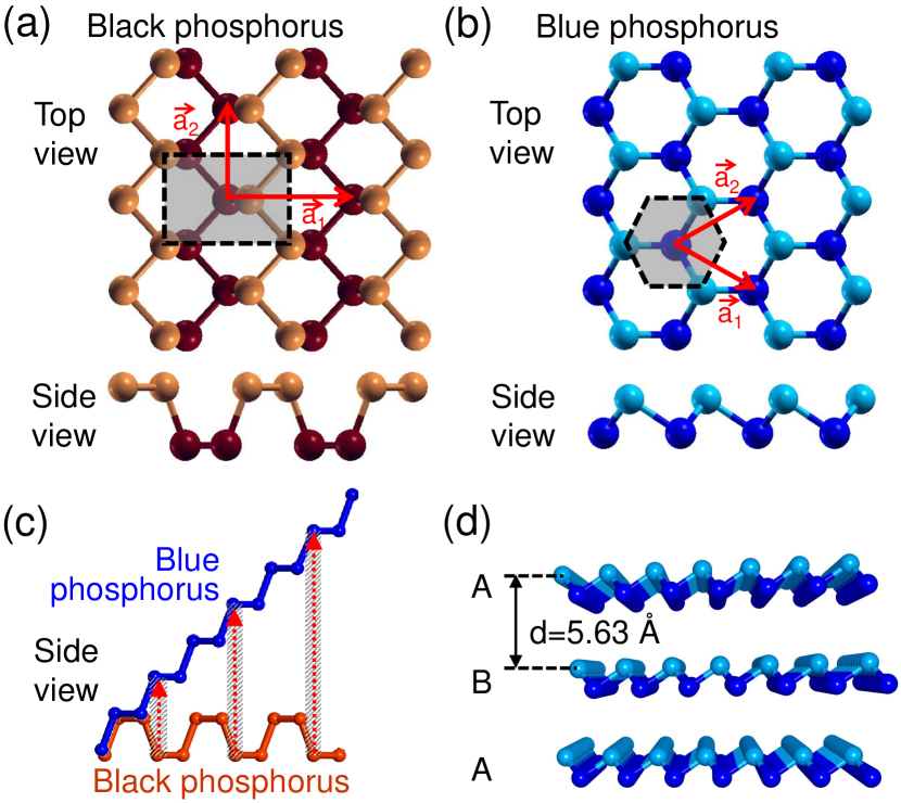
The optimized reference structure of black phosphorus, shown in Fig. 1(a), is presented next to the proposed blue phosphorus structure in Fig. 1(b). The top view of both structures illustrates their similarity with the honeycomb lattice of graphite, which contains two atoms per layer per unit cell. Both phosphorus allotropes differ from graphite in the non-planar structure of their layers. In top view, the isotropic structure of blue phosphorus in Fig. 1(b) differs significantly from the anisotropic structure of black phosphorus in Fig. 1(a). As seen in side view in Figs. 1(a) and 1(b), the puckered zigzag structure in the cross-section of blue phosphorus differs from the distinct armchair ridges that cause the anisotropy of black phosphorus. The puckering in the blue phosphorus monolayer is similar to the postulated structure of single-wall phosphorus nanotubesSeifert and Hernández (2000).
The structural relationship between blue and black phosphorus is illustrated schematically in Fig. 1(c). A dislocation is introduced in a monolayer of black phosphorus by flipping specific P atoms from a ‘down’ to an ‘up’ position without changing the local bond angles, as described below and indicated by the arrows in Fig. 1(c). Subjecting every fourth row of P atoms to this transformation converts a monolayer of black to blue phosphorus. The location of dislocation lines in the monolayer structures is emphasized by the shaded regions in Fig. 1(c).
Atoms in the layers of blue phosphorus are covalently bonded at the equilibrium distance of 2.27 Å, resulting in a large binding energy of 5.19 eV/atom. This value differs from that of black phosphorus by less than meV/atom, suggesting that blue and black phosphorus are equally stable. A weak inter-layer interactionSM- of 6 meV/atom holds the layered structure together at the interlayer distance Å, as seen in Fig. 1(d), which indicates the possibility of easy exfoliation. The AB hexagonal stacking and the ABC rhombohedral stacking of layers differ energetically by less than meV/atom.
The optimized hexagonal unit cell of an isolated blue phosphorus monolayer, shown in Fig. 1(b), is spanned by lattice vectors and , with Å. The influence of the interlayer interaction on the in-layer structure is small, causing only a negligible change from Å in the bulk to Å in the isolated monolayer. With its higher symmetry, the smaller hexagonal Wigner-Seitz cell of blue phosphorus, which contains two atoms and is shown in Fig. 1(b), differs from the rectangular Wigner-Seitz cell of the anisotropic black phosphorus monolayer with 4 atoms/unit cell, as shown in Fig. 1(a). Still, monolayers of blue and black phosphorus may form an ‘ideal’ in-layer connection by the dislocation illustrated in Fig. 1(c).

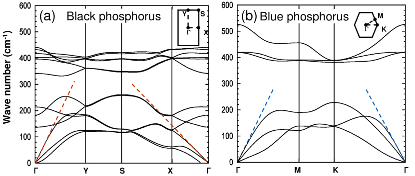
One way to compare the stability and structural rigidity of the different phosphorus allotropes is by studying the vibration spectrum. Our results for the vibration spectra of blue and black phosphorus monolayers are presented in Fig. 2. We find the vibration spectra to be rather similar, reflecting a very similar bonding character. Acoustic and optical modes are well separated in both black and blue phosphorus. The harder longitudinal optical modes reflect a higher in-plane rigidity of the blue phosphorus allotrope in comparison to the accordion-like black phosphorus structure. The calculated flexural rigidity value eV in blue phosphorus is lower than the eV value in black phosphorus. These values provide a quantitative explanation for the dispersion of the flexural acoustic modes ZA near the pointSánchez-Portal et al. (1999) in the two allotropesSM- . The high rigidity of a free-standing blue phosphorus monolayer was also confirmed by our molecular dynamics calculations at nonzero temperatures, discussed in the Supplemental MaterialSM- .

We next compare the slopes of the longitudinal acoustic branches near , which correspond to the speed of sound and reveal the in-plane stiffness. As seen in Fig. 2(a), the speed of sound along the direction in black phosphorus, km/s, is significantly higher than the km/s value along the direction, reflecting an anisotropy in the elastic constants. The lower rigidity along the direction, corresponding to the direction in Fig. 1(a), reflects the fact that compression along requires primarily bond bending, which comes at a lower energy cost than bond stretching. In strong contrast to those findings, our results in Fig. 2(b) indicate that the in-plane elastic response of blue phosphorus is nearly isotropic, with nearly the same value km/s for the speed of sound along the and the direction. The predicted finite in-layer compressibility of these non-planar structures is advantageous when accommodating lattice mismatch during Chemical Vapor Deposition (CVD) growth on a substrate.
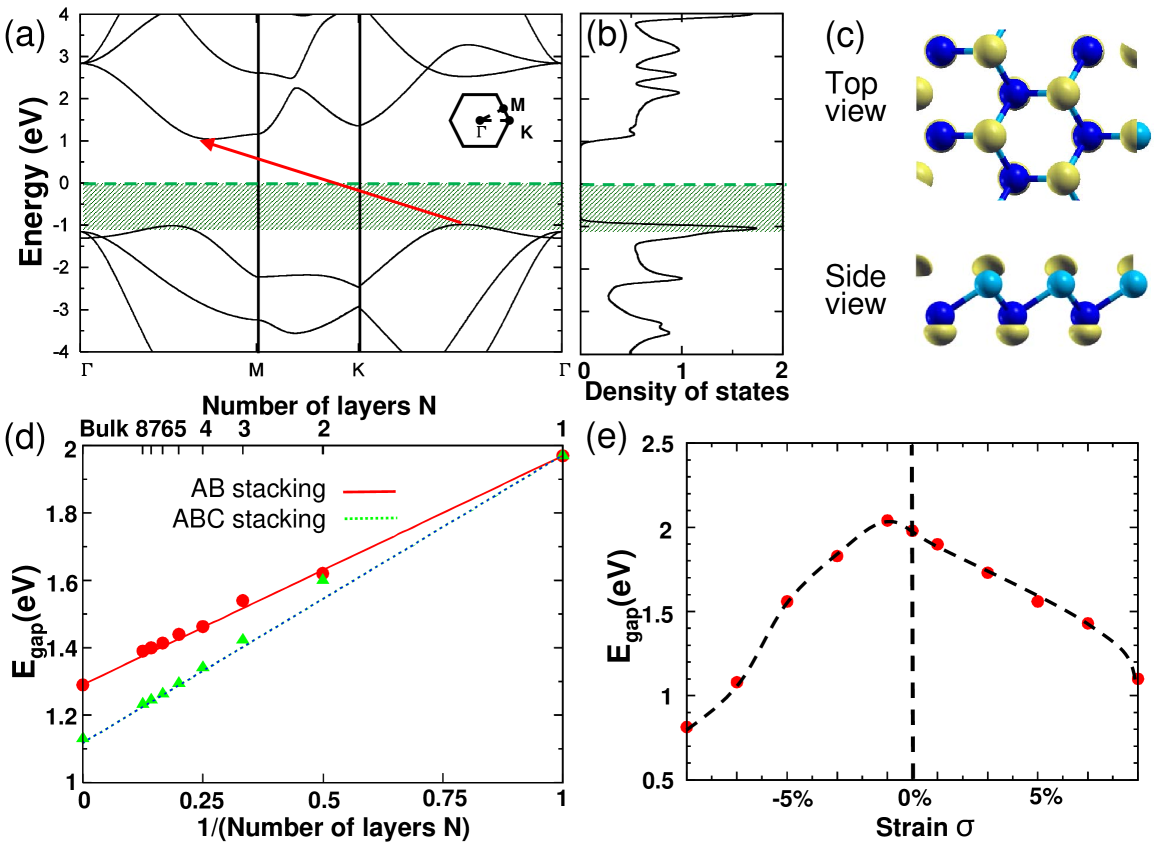
Our DFT results for the electronic structure of blue phosphorus are presented in Fig. 3. The calculated band structure and density of states, presented in Figs. 3(a) and 3(b), indicate that a blue phosphorus monolayer is a semiconductor with an indirect band gap eV. Comparison with more proper self-energy calculations based on the GW approach, performed by VASP, indicate that the DFT band gap is underestimated by eV in mono- and multi-layers of blue P as a common shortcoming of DFT. Still, the electronic structure of the valence and the conduction band region in DFT is believed to closely represent experimental results. Therefore, we expect the charge density associated with states near the top of the valence band, shown in Fig. 3(c), to be represented accurately. These states correspond to the energy range highlighted by the green shading in Figs. 3(a) and 3(b), which extends from mid-gap to 0.1 eV below the top of the valence band. These states cause the inter-layer band dispersion in few-layer systemsSM- , and their hybrids with electronic states of the contact electrodes will play a crucial role in the carrier injection and quantum transport.
More interesting than the precise value of the fundamental band gap is its dependence on the number of layers in a multi-layer slab, shown in Fig. 3(d). This is a consequence of the inter-layer dispersion near the Fermi level in the bulk material, which is discussed in the Supplemental MaterialSM- . Independent of the type of stacking, we find to be inversely proportional to between one monolayer and the bulk structure. We conclude that modifying the slab thickness may change the value of by up to a factor of 2, which is very important for electronic applications. The -dependent band gap value of eV lies just above the photon energy of visible blue light. We derive the name ‘blue phosphorus’ from this absorption edge, which plays a key role in the optical appearance.
As seen in Fig. 3(e), the band gap depends also sensitively on the applied in-layer strain . In view of the non-planarity of the structure, the discussed strain range can be achieved without a large energy penalty, as discussed in connection with the vibration spectra. The possibility to change the band gap value by in strained epitaxial geometries on different substrates is one more indication that blue phosphorus may find intriguing applications in nanoelectronics.

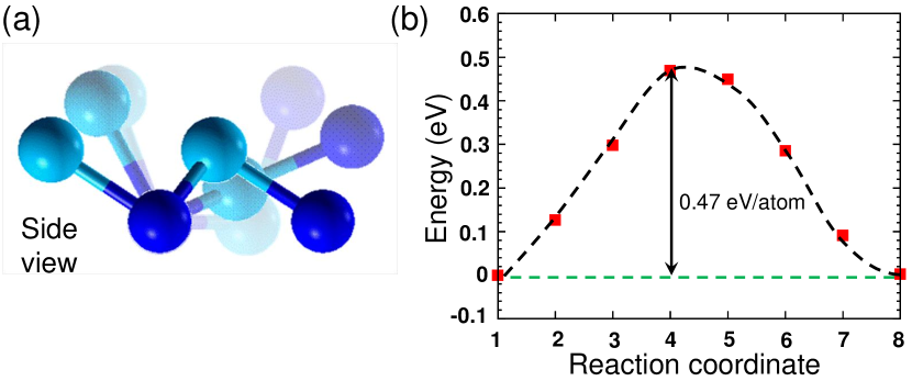
We next studied the possibility of converting a monolayer of black to blue phosphorus by introducing an array of dislocations, depicted schematically in Fig. 1(c). Our discussion of the conversion process including energy estimates is presented in Fig. 4 and the Supplemental MaterialSM- . The starting black phosphorus, the final blue phosphorus, and an intermediate structure are depicted in side view in Fig. 4(a). To estimate changes in the atomic arrangement during the conversion process, we changed and constrained the out-of-plane displacement of specific atoms in the unit cell to follow the ‘black-to-blue’ trajectory and relaxed all other degrees of freedom. This provided us with a sequence of structures ‘1-8’ in-between black and blue phosphorus, which loosely define the reaction coordinate in Fig. 4(b). The change in the unit cell from black to blue phosphorus has been imposed between steps ‘1’ and ‘2’ by deforming it from the initial size and shape in black phosphorus to the final rectangular supercell in blue phosphorus, followed by atomic relaxation. Our results for the relative energy with respect to the black phosphorus structure ‘1’ again illustrate our finding that the blue phosphorus structure ‘8’ is equally stable as ‘1’. The activation barrier for the conversion process is likely overestimated due to the constraints imposed on the intermediate structures and may further be lowered by stretching black phosphorus layers. Thus the true value should be below the already low value of eV/atom, indicating the relative ease of mechanical conversion from black to blue phosphorus.
As suggested earlier, the weak inter-layer interaction should allow mechanical exfoliation of blue phosphorus in analogy to the black allotropeLiu et al. (2014). As a matter of fact, depositing mechanically a monolayer of black phosphorus onto a stepped substrate may cause formation of dislocation lines and thus formation of narrow domains of blue phosphorus in the monolayer structure along the step edges of the substrate. In analogy to grapheneKim et al. (2009); Reina et al. (2009) and siliceneVogt et al. (2012), also layered phosphorus structures may be grown by CVD on specific substrates. As suggested in this study, blue and black phosphorus should be equally stable. The preferential phase should thus be determined by the lattice constant and the symmetry of the substrate in order to maximize the adsorption energy. Consequently, we expect blue phosphorus to form preferentially on substrates with hexagonal symmetry and a matching lattice constant, such as MoS2, or the (0001) surfaces of Zr and Sc, whereas black phosphorus should start growing on substrates with a rectangular lattice. Due to the low energy of forming a dislocation that connects blue and black phosphorus, both allotropes could coexist on particular substrates, including stepped surfaces, to optimize the adlayer-substrate interaction.
One of the main reasons for the interest in 2D semiconductors including graphene for electronic applications is the observed high mobility of carriers. Related quasi-2D systems, including MoS2, bring the benefit of a nonzero band gap, but display lower intrinsic carrier mobility due to enhanced electron-phonon coupling, primarily caused by the presence of heavy elements such as MoPerera et al. (2013). It appears likely that the blue phosphorus structure, similar to black phosphorusLiu et al. (2014), may exhibit a higher carrier mobility than MoS2. The combination of a significant band gap and high carrier mobility would turn blue phosphorus into an excellent contender for a new generation of nano-electronic devices.
In conclusion, we have conducted ab initio calculations to investigate a previously unknown layered phase of phosphorus, which we call ‘blue phosphorus’. We find blue phosphorus to be nearly as stable as black phosphorus, the most stable phosphorus allotrope. While sharing the atomic connectivity with the honeycomb lattice of graphene, layers of blue phosphorus are non-planar. Whereas the bulk layer stacking of blue phosphorus is closely related to graphite, the main advantage of this allotrope is its wide fundamental band gap in excess of 2 eV. Due to the weak inter-layer interaction, blue phosphorus should exfoliate easily to form quasi-2D structures for potential electronic applications. We have investigated a likely transformation pathway from black to blue phosphorus and show that the postulated structure may form spontaneously by CVD on a lattice-matched substrate or may be result by stretching black phosphorus. Monolayers of blue phosphorus may form a structurally ideal connection to monolayers of black phosphorus with a different electronic structure.
Acknowledgements.
We thank Peide Ye for directing our attention towards the related black phosphorus structure. This study was supported by the National Science Foundation Cooperative Agreement #EEC-0832785, titled “NSEC: Center for High-rate Nanomanufacturing”. Computational resources have been provided by the Michigan State University High Performance Computing Center.Note added in proof.—We have learned that blue phosphorus is structurally related to the postulatedBoulfelfel et al. (2012) and observedJamieson (1963) phase of phosphorus.
References
- Hultgren et al. (1935) R. Hultgren, N. S. Gingrich, and B. E. Warren, J. Chem. Phys. 3, 351 (1935).
- Thurn and Kerbs (1966) H. Thurn and H. Kerbs, Angew. Chem. Internat. Edit. 5, 1047 (1966).
- Maruyama et al. (1981) Y. Maruyama, S. Suzuki, K. Kobayashi, and S. Tanuma, Physica B+C 105, 99 (1981).
- Narita et al. (1983) S. Narita, Y. Akahama, Y. Tsukiyama, K. Muro, S. Mori, S. Endo, M. Taniguchi, M. Seki, S. Suga, A. Mikuni, and H. Kanzaki, Physica B+C 117&118, 422 (1983).
- Artacho et al. (2008) E. Artacho, E. Anglada, O. Dieguez, J. D. Gale, A. Garcia, J. Junquera, R. M. Martin, P. Ordejon, J. M. Pruneda, D. Sanchez-Portal, and J. M. Soler, J. Phys. Cond. Mat. 20, 064208 (2008).
- Kresse and Furthmüller (1996) G. Kresse and J. Furthmüller, Phys. Rev. B 54, 11169 (1996).
- Perdew et al. (1996) J. P. Perdew, K. Burke, and M. Ernzerhof, Phys. Rev. Lett. 77, 3865 (1996).
- Troullier and Martins (1991) N. Troullier and J. L. Martins, Phys. Rev. B 43, 1993 (1991).
- Monkhorst and Pack (1976) H. J. Monkhorst and J. D. Pack, Phys. Rev. B 13, 5188 (1976).
- Hestenes and Stiefel (1952) M. R. Hestenes and E. Stiefel, J. Res. Natl. Bur. Stand. 49, 409 (1952).
-
(11)
See Supplemental Material at
http://link.aps.org/
supplemental/10.1103/PhysRevLett.000.000000 for details regarding bulk structure, bonding and vibration modes, as well as molecular dynamics simulations of blue phosphorus monolayers at elevated temperatures. - Seifert and Hernández (2000) G. Seifert and E. Hernández, Chem. Phys. Lett. 318, 355 (2000).
- Sánchez-Portal et al. (1999) D. Sánchez-Portal, E. Artacho, J. M. Soler, A. Rubio, and P. Ordejón, Phys. Rev. B 59, 12678 (1999).
- Liu et al. (2014) H. Liu, A. Neal, Z. Zhu, D. Tománek, and P. Ye, “Phosphorene: a new high-mobility 2d semiconductor,” (2014), arXiv:1401.4133 .
- Kim et al. (2009) K. S. Kim, Y. Zhao, H. Jang, S. Y. Lee, J. M. Kim, K. S. Kim, J.-H. Ahn, P. Kim, J.-Y. Choi, and B. H. Hong, Nature 457, 706 (2009).
- Reina et al. (2009) A. Reina, X. Jia, J. Ho, D. Nezich, H. Son, V. Bulovic, M. S. Dresselhaus, and J. Kong, Nano Lett. 9, 30 (2009).
- Vogt et al. (2012) P. Vogt, P. De Padova, C. Quaresima, J. Avila, E. Frantzeskakis, M. C. Asensio, A. Resta, B. Ealet, and G. Le Lay, Phys. Rev. Lett. 108, 155501 (2012).
- Perera et al. (2013) M. M. Perera, M.-W. Lin, H.-J. Chuang, B. P. Chamlagain, C. Wang, X. Tan, M. M.-C. Cheng, D. Tománek, and Z. Zhou, ACS Nano 7, 4449 (2013).
- Boulfelfel et al. (2012) S. E. Boulfelfel, G. Seifert, Y. Grin, and S. Leoni, Phys. Rev. B 85, 014110 (2012).
- Jamieson (1963) J. C. Jamieson, Science 139, 1291 (1963).