refReferences
Transformation Optics scheme for two-dimensional materials
Abstract
Two dimensional optical materials, such as graphene can be characterized by a surface conductivity. So far, the transformation optics schemes have focused on three dimensional properties such as permittivity and permeability . In this paper, we use a scheme for transforming surface currents to highlight that the surface conductivity transforms in a way different from and . We use this surface conductivity transformation to demonstrate an example problem of reducing scattering of plasmon mode from sharp protrusions in graphene.
pacs:
(160.3918) Metamaterials; (230.3205) Invisibility cloaks; (240.6680) Surface plasmons.Transformation opticsPendry03082012 ; doi:10.1021/nl100800c has proved to be a powerful technique to control propagation of electromagnetic waves. The basic idea is that under coordinate transformations, Maxwell’s equations remain form-invariant, provided the material parameters are appropriately modified. Then the wave electromagnetic wave propagation in the transformed medium can be thought of as occurring in the original medium. Numerous applications of this technique have been proposed and demonstrated. Some examples are invisiblity cloaksSchurig10112006 ; Liu16012009 ; DielectricCloak , waveguides with sharp bendsroberts:251111 , subwavelength image manipulationSchurig:07 , etc.
With the recent discovery of two dimensional materials such as graphenedoi:10.1038/nmat1849 and MoS2MoS2review ; PhysRevLett.105.136805 , there is an enormous interest in studying their optical propertiesHamm14062013 . Such materials are usually characterized by a surface conductivity instead of the volume conductivity which describes the usual three dimensional materials. As such it is expected that the techniques of transformation optics, as is usually employed, will have to be modified to take into account the change in the dimensionality of the material parameter. To our knowledge, this is the first time that a full transformation optics scheme involving surface conductivity has been considered. Although implementing transformation optics using spatial modulation of surface conductivity has been proposed in GrapheneTransfOptics , we note that they do not talk about transformations which can take the graphene out of the plane. In other words, they only consider flat graphene.
In this paper, we will show how surface conductivity transforms under arbitrary coordinate transformations. We will find that the transformation rule is indeed different compared to the bulk conductivity. Then we will present an example to show how this surface conductivity transformation works for the simple case of a two dimensional transformation. We show how to reduce plasmon scattering from a triangular protrusion in graphene. It is indeed possible to implement such a surface conductivity transformation in graphene using gate voltage10.1126/science.1102896 and chemical doping.
Let us consider the case of a 2D material sitting in between two dielectric materials. The source free Ampère’s Law is written in this case as:
| (1) |
where is the equation of the surface discontinuity, is the permittivity of the surrounding three dimensional materials and is the surface polarization of the two dimensional material. The time derivative of this surface polarization gives rise to a surface current density:
| (2) |
For the usual case of the interface of two bulk materials, this term is absent, however for 2D materials we need to retain this term in the derivation of the boundary conditions due to the presence of the Dirac delta function in Eq.1. Thus, in this case of a finite surface electrical conductivity , the boundary condition for the tangential magnetic field can be written in terms of a surface currentPhysRevB.80.245435
| (3) |
where is the surface current density, is the unit normal to the surface and is the surface conductivity tensor. For instance, an isotropic surface conductivity would be represented in terms of the basis {, , }, as . Here and are the two orthonormal local tangential vectors and is the local normal unit vector. Our aim here is to find out the transformation rule for the tensor.
Based on Eq.1 and 2, the permittivity can be thought of as containing a Dirac delta function:
| (4) |
Now, applying the usual transformation rule for permittivity to Eq.4 and the standard rule for the change of variables in a delta function, we arrive at the result:
| (5) |
where is the local surface normal given by and is the transformation matrix . The additional factor explicitly enters the surface conductivity tensor because a compression in the plane normal for the 2D material, should produce no transformation of the surface conductivity physically. But the factor does contain this compression factor. Therefore surface conductivity further requires a multiplicative factor for the renormalization of the surface delta function. Equivalently, one could say that the normal unit vector, after transformation, does not remain a unit vector. Hence the additional factor needs to be put in to ensure that in the transformed medium, is indeed a unit vector.
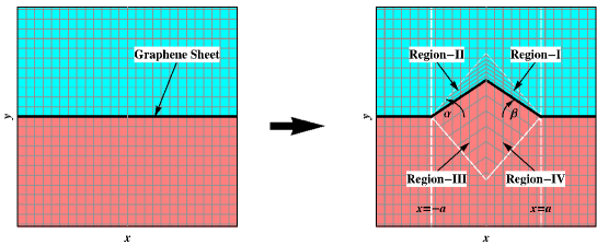
Taking cue from the SPP wave adapter proposed in doi:10.1021/nn200516r ; Arigong:12 , we illustrate that the surface conductivity transformation indeed works, by using the transformation shown in Fig.1.
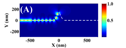
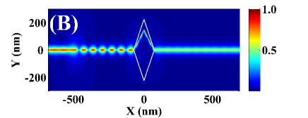
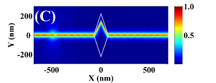
In the absence of any transformation optics, the plasmon mode propagating along the graphene sheet from the far left, would suffer substantial scattering into the free space modes. Such radiative loss is typically dependent on the radius of curvature of the bump. For instance, if the graphene plasmon mode is highly confined compared to the radius of curvature of the bump, then it is possible to achieve smaller radiative loss of the plasmon modeLu:13 . In our current formalism however, we are able to tackle arbitrary radii of curvatures. To subvert this scattering one can employ the well known technique of transformation optics. This scheme would require us to modify the permittivity and permeability tensors in the region surrounding the sharp bump. However, just this would not be enough to prevent scattering since as we mentioned earlier, the surface conductivity also needs to be transformed in a way which depends on the details of the transformation we wish to carry out.
Hence we consider three cases: A) protrusion in graphene with no transformation optics employed, B) transformation optics employed but surface conductivity is not transformed and C) transformation optics employed for the surface conductivity as well as the bulk parameters. The results are shown in Fig.2. Finite element simulations in Fig.2 were carried out using comsol multiphysics by employing a surface current boundary condition to represent the graphene. The surrounding media in the un-transformed case is assumed to be vacuum, for this example. But we have performed tests, which are not presented here with substrates of non-unity refractive indices as well. For simplicity we use only the imaginary part of the surface conductivity of graphene at a doping level of eV at zero temperature. The excitation frequency for this test case is eV, so the numerical value of the in-plane untransformed surface conductivity is .
Mathematically, the transformation in the four regions shown in Fig.1 is given as follows:
| (6) | |||
Everywhere outside the four regions, there is no change. Note that we have chosen a linear map only for the purpose of demonstration of the main idea of surface conductivity transformation. The transformation we provided in Eq.5 is valid in general, beyond the linear approximation. In principle, other transformations can be employed keeping in mind the material constraints. For instance, quasi-conformal mapsPhysRevLett.101.203901 which have been applied in the context of plasmonics elsewhere:/content/aip/journal/jap/114/14/10.1063/1.4824280 , could be employed; or, in the case of rotationally symmetric three dimensional bumps of various shapes, it might be possible to design isotropic graphene-surface conductivity and the environment-permittivity profile obtained using techniques similar to PhysRevLett.111.213901 .
The Jacobian is given by:
| (7) |
Then the transformed bulk material parameters in the four regions are given, in the basis, as follows:
| (8) |
The new surface conductivity tensor is expressed using Eq.5, with , as
| (9) |
where is the scalar surface conductivity of the untransformed graphene.
Now, from Eq.9, it might appear that the surface conductivity tensor has off-diagonal components, which would be difficult to achieve experimentally. However, one must remember that the transformed tensor is given in the basis. To get more physical insight, we go the basis, where is a unit vector locally tangential to the graphene and is locally normal to graphene surface. Since the direction is unchanged in this example, we keep the same unit vector in that direction. A basis change can be carried out using , where is the basis change matrix composed of projections of the new basis vectors on the old basis vectors. In our case, graphene is situated in regions I and II, for which the matrix is given by
| (10) |
Then is given by
| (11) |
Two things are apparent from the form of in Eq.11. Firstly, there is a geometrical scaling factor involved in the transformed conductivity tensor. In particular, for the untransformed case, the components and should both be equal to . These geometrical factors can be understood in terms of surface current conservation, as pointed out in PhysRevA.80.033820 . The surface current density in the tangential direction prior to the transformation is . After the transformation it becomes . For the direction, we note that it is the surface current that needs to be preserved across the region . So we have, .
Secondly, it appears here that the given transformation requires us to somehow make the graphene conductivity anisotropic, that is, and need to be different. Although it might be possible to achieve such anisotropic effects using strained graphene0295-5075-92-6-67001 ; PhysRevB.81.035411 ; wright:163104 ; JMR:8477871 , yet in the present case of TM modes, component does not matter since the boundary condition for only involves the surface current in the direction. Hence this conductivity change can be easily implemented via electrostatic:/content/aip/journal/apl/100/5/10.1063/1.3681799 or chemical doping. As far as the bulk parameters, namely are concerned, there have been numerous demonstrations of natural and artificial anisotropic materials in the THz rangebao:031910 ; bychanok:114304 ; ADMA:ADMA201103890 ; srep00078 .
We have demonstrated the transformation rule for surface conductivity under arbitrary coordinate transformations. An additional factor related to the re-normalization of the surface current needs to be included to maintain the form invariance of the Maxwell’s equations. We then presented an example problem of reducing scattering from a triangular protrusion in graphene, using the proposed method of surface conductivity transformation. This kind of conductivity transformation would be useful for transformation optics applications involving two dimensional materials.
A.K. and N.X.F. acknowledge the financial support by the NSF (grant CMMI-1120724) and AFOSR MURI (Award No. FA9550-12-1-0488). K.H.F. acknowledges financial support from Hong Kong RGC grant 509813. We thank Professor Steven G. Johnson for helpful suggestions.
osajnl_without_title
References
- (1) J. B. Pendry, A. Aubry, D. R. Smith, and S. A. Maier, Science 337, 549–552 (2012).
- (2) P. A. Huidobro, M. L. Nesterov, L. Martín-Moreno, and F. J. García-Vidal, Nano Letters 10, 1985–1990 (2010). PMID: 20465271.
- (3) D. Schurig, J. J. Mock, B. J. Justice, S. A. Cummer, J. B. Pendry, A. F. Starr, and D. R. Smith, Science 314, 977–980 (2006).
- (4) R. Liu, C. Ji, J. J. Mock, J. Y. Chin, T. J. Cui, and D. R. Smith, Science 323, 366–369 (2009).
- (5) J. Valentine, J. Li, T. Zentgraf, G. Bartal, and X. Zhang, Nature Materials 8, 568–571 (2009).
- (6) D. A. Roberts, M. Rahm, J. B. Pendry, and D. R. Smith, Applied Physics Letters 93, 251111 (2008).
- (7) D. Schurig, J. B. Pendry, and D. R. Smith, Opt. Express 15, 14772–14782 (2007).
- (8) A. K. Geim and K. S. Novoselov, Nature Materials 6, 183–191 (2007).
- (9) Q. H. Wang, K. Kalantar-Zadeh, A. Kis, J. N. Coleman, and M. S. Strano, Nature Nanotechnology 7, 699–712 (2012).
- (10) K. F. Mak, C. Lee, J. Hone, J. Shan, and T. F. Heinz, Phys. Rev. Lett. 105, 136805 (2010).
- (11) J. M. Hamm and O. Hess, Science 340, 1298–1299 (2013).
- (12) A. Vakil and N. Engheta, Science 332, 1291–1294 (2011).
- (13) K. S. Novoselov, A. K. Geim, S. V. Morozov, D. Jiang, Y. Zhang, S. V. Dubonos, I. V. Grigorieva, and A. A. Firsov, Science 306, 666–669 (2004).
- (14) M. Jablan, H. Buljan, and M. Soljačić, Phys. Rev. B 80, 245435 (2009).
- (15) J. Zhang, S. Xiao, M. Wubs, and N. A. Mortensen, ACS Nano 5, 4359–4364 (2011).
- (16) B. Arigong, J. Shao, H. Ren, G. Zheng, J. Lutkenhaus, H. Kim, Y. Lin, and H. Zhang, Opt. Express 20, 13789–13797 (2012).
- (17) W. B. Lu, W. Zhu, H. J. Xu, Z. H. Ni, Z. G. Dong, and T. J. Cui, Opt. Express 21, 10475–10482 (2013).
- (18) J. Li and J. B. Pendry, Phys. Rev. Lett. 101, 203901 (2008).
- (19) B. Arigong, J. Ding, H. Ren, R. Zhou, H. Kim, Y. Lin, and H. Zhang, Journal of Applied Physics 114, 144301 (2013).
- (20) R. C. Mitchell-Thomas, T. M. McManus, O. Quevedo-Teruel, S. A. R. Horsley, and Y. Hao, Phys. Rev. Lett. 111, 213901 (2013).
- (21) S. A. Cummer, N. Kundtz, and B.-I. Popa, Phys. Rev. A 80, 033820 (2009).
- (22) V. M. Pereira, R. M. Ribeiro, N. M. R. Peres, and A. H. C. Neto, EPL (Europhysics Letters) 92, 67001 (2010).
- (23) F. M. D. Pellegrino, G. G. N. Angilella, and R. Pucci, Phys. Rev. B 81, 035411 (2010).
- (24) A. R. Wright and C. Zhang, Applied Physics Letters 95, 163104 (2009).
- (25) Y. Liang, S. Huang, and L. Yang, Journal of Materials Research pp. 403–409 (2012).
- (26) H. Ju Xu, W. Bing Lu, Y. Jiang, and Z. Gao Dong, Applied Physics Letters 100, 051903 (2012).
- (27) Y. Bao, C. He, F. Zhou, C. Stuart, and C. Sun, Applied Physics Letters 101, 031910 (2012).
- (28) D. S. Bychanok, M. V. Shuba, P. P. Kuzhir, S. A. Maksimenko, V. V. Kubarev, M. A. Kanygin, O. V. Sedelnikova, L. G. Bulusheva, and A. V. Okotrub, Journal of Applied Physics 114, 114304 (2013).
- (29) D. Liang, J. Gu, J. Han, Y. Yang, S. Zhang, and W. Zhang, Advanced Materials 24, 916–921 (2012).
- (30) F. Zhou, Y. Bao, W. Cao, C. T. Stuart, J. Gu, and C. Sun, Scientific Reports 1 (2011).
osajnl \bibliographyrefOpexStyle
References
- (1) J. B. Pendry, A. Aubry, D. R. Smith, and S. A. Maier, “Transformation optics and subwavelength control of light,” Science 337, 549–552 (2012).
- (2) P. A. Huidobro, M. L. Nesterov, L. Martín-Moreno, and F. J. García-Vidal, “Transformation optics for plasmonics,” Nano Letters 10, 1985–1990 (2010). PMID: 20465271.
- (3) D. Schurig, J. J. Mock, B. J. Justice, S. A. Cummer, J. B. Pendry, A. F. Starr, and D. R. Smith, “Metamaterial electromagnetic cloak at microwave frequencies,” Science 314, 977–980 (2006).
- (4) R. Liu, C. Ji, J. J. Mock, J. Y. Chin, T. J. Cui, and D. R. Smith, “Broadband ground-plane cloak,” Science 323, 366–369 (2009).
- (5) J. Valentine, J. Li, T. Zentgraf, G. Bartal, and X. Zhang, “An optical cloak made of dielectrics,” Nature Materials 8, 568–571 (2009).
- (6) D. A. Roberts, M. Rahm, J. B. Pendry, and D. R. Smith, “Transformation-optical design of sharp waveguide bends and corners,” Applied Physics Letters 93, 251111 (2008).
- (7) D. Schurig, J. B. Pendry, and D. R. Smith, “Transformation-designed optical elements,” Opt. Express 15, 14772–14782 (2007).
- (8) A. K. Geim and K. S. Novoselov, “The rise of graphene,” Nature Materials 6, 183–191 (2007).
- (9) Q. H. Wang, K. Kalantar-Zadeh, A. Kis, J. N. Coleman, and M. S. Strano, “Electronics and optoelectronics of two-dimensional transition metal dichalcogenides,” Nature Nanotechnology 7, 699–712 (2012).
- (10) K. F. Mak, C. Lee, J. Hone, J. Shan, and T. F. Heinz, “Atomically thin : A new direct-gap semiconductor,” Phys. Rev. Lett. 105, 136805 (2010).
- (11) J. M. Hamm and O. Hess, “Two two-dimensional materials are better than one,” Science 340, 1298–1299 (2013).
- (12) A. Vakil and N. Engheta, “Transformation optics using graphene,” Science 332, 1291–1294 (2011).
- (13) K. S. Novoselov, A. K. Geim, S. V. Morozov, D. Jiang, Y. Zhang, S. V. Dubonos, I. V. Grigorieva, and A. A. Firsov, “Electric field effect in atomically thin carbon films,” Science 306, 666–669 (2004).
- (14) M. Jablan, H. Buljan, and M. Soljačić, “Plasmonics in graphene at infrared frequencies,” Phys. Rev. B 80, 245435 (2009).
- (15) J. Zhang, S. Xiao, M. Wubs, and N. A. Mortensen, “Surface plasmon wave adapter designed with transformation optics,” ACS Nano 5, 4359–4364 (2011).
- (16) B. Arigong, J. Shao, H. Ren, G. Zheng, J. Lutkenhaus, H. Kim, Y. Lin, and H. Zhang, “Reconfigurable surface plasmon polariton wave adapter designed by transformation optics,” Opt. Express 20, 13789–13797 (2012).
- (17) W. B. Lu, W. Zhu, H. J. Xu, Z. H. Ni, Z. G. Dong, and T. J. Cui, “Flexible transformation plasmonics using graphene,” Opt. Express 21, 10475–10482 (2013).
- (18) J. Li and J. B. Pendry, “Hiding under the carpet: A new strategy for cloaking,” Phys. Rev. Lett. 101, 203901 (2008).
- (19) B. Arigong, J. Ding, H. Ren, R. Zhou, H. Kim, Y. Lin, and H. Zhang, “Design of wide-angle broadband luneburg lens based optical couplers for plasmonic slot nano-waveguides,” Journal of Applied Physics 114, 144301 (2013).
- (20) R. C. Mitchell-Thomas, T. M. McManus, O. Quevedo-Teruel, S. A. R. Horsley, and Y. Hao, “Perfect surface wave cloaks,” Phys. Rev. Lett. 111, 213901 (2013).
- (21) S. A. Cummer, N. Kundtz, and B.-I. Popa, “Electromagnetic surface and line sources under coordinate transformations,” Phys. Rev. A 80, 033820 (2009).
- (22) V. M. Pereira, R. M. Ribeiro, N. M. R. Peres, and A. H. C. Neto, “Optical properties of strained graphene,” EPL (Europhysics Letters) 92, 67001 (2010).
- (23) F. M. D. Pellegrino, G. G. N. Angilella, and R. Pucci, “Strain effect on the optical conductivity of graphene,” Phys. Rev. B 81, 035411 (2010).
- (24) A. R. Wright and C. Zhang, “Stretching induced hall current and conductance anisotropy in graphene,” Applied Physics Letters 95, 163104 (2009).
- (25) Y. Liang, S. Huang, and L. Yang, “Many-electron effects on optical absorption spectra of strained graphene,” Journal of Materials Research pp. 403–409 (2012).
- (26) H. Ju Xu, W. Bing Lu, Y. Jiang, and Z. Gao Dong, “Beam-scanning planar lens based on graphene,” Applied Physics Letters 100, 051903 (2012).
- (27) Y. Bao, C. He, F. Zhou, C. Stuart, and C. Sun, “A realistic design of three-dimensional full cloak at terahertz frequencies,” Applied Physics Letters 101, 031910 (2012).
- (28) D. S. Bychanok, M. V. Shuba, P. P. Kuzhir, S. A. Maksimenko, V. V. Kubarev, M. A. Kanygin, O. V. Sedelnikova, L. G. Bulusheva, and A. V. Okotrub, “Anisotropic electromagnetic properties of polymer composites containing oriented multiwall carbon nanotubes in respect to terahertz polarizer applications,” Journal of Applied Physics 114, 114304 (2013).
- (29) D. Liang, J. Gu, J. Han, Y. Yang, S. Zhang, and W. Zhang, “Robust large dimension terahertz cloaking,” Advanced Materials 24, 916–921 (2012).
- (30) F. Zhou, Y. Bao, W. Cao, C. T. Stuart, J. Gu, and C. Sun, “Hiding a realistic object using a broadband terahertz invisibility cloak,” Scientific Reports 1 (2011).