Electron Transport in MoWSeS Monolayers in Presence of an External Electric Field
Abstract
The influence of an external electric field on single-layer transition-metal dichalcogenides TX2 with T = Mo, W and X = S, Se (MoWSeS) have been investigated by means of density-functional theory within two-dimensional periodic boundary conditions under consideration of relativistic effects including the spin-orbit interactions. Our results show that the external field modifies the band structure of the monolayers, in particular the conduction band. This modification has, however, very little influence on the band gap and effective masses of holes and electrons at the point, and also the spin-orbit splitting of these monolayers is almost unaffected. Our results indicate a remarkable stability of the electronic properties of TX2 monolayers with respect to gate voltages. A reduction of the electronic band gap is observed only starting from field strengths of 2.0 V Å-1 (3.5 V Å-1) for selenides (sulphides), and the transition to a metallic phase would occur at fields of 4.5 Å-1 (6.5 Å-1).
Monolayered transition-metal dichalcogenides, such as TX2 with T = Mo, W and X = S, Se (MoWSeS), have emerged as novel attractive two dimensional (2D) materials for potential applications in nano- and optoelectronic devices.Wang et al. (2012) TX2 of 2 symmetry are hexagonal systems with one layer of transition-metal atoms sandwiched between two layers of chalcogen atoms. In the bulk form, the adjacent sheets are held together via weak interlayer forces, thus allowing easy and fast mechanical or chemical exfoliation to the monolayered forms.Mak et al. (2010); Radisavljevic et al. (2011); Coleman et al. (2011) Recently, Kis and co-workers have made a substantial breakthrough by using MoS2 monolayers to fabricate field-effect transistors,Radisavljevic et al. (2011) integrated circuitsRadisavljevic et al. (2011), amplifiersRadisavljevic et al. (2012) and photodetectors.Lopez-Sanchez et al. (2013)
Semiconducting MoWSeS materials undergo the indirect to direct band gap transition when thinned to the monolayer limit.Splendiani et al. (2010); Mak et al. (2010); Kuc et al. (2011) At this limit, the inversion symmetry is lost what causes a giant spin-orbit-induced band splitting of 100 meV for MoS2 monolayer from Raman experiments,Sun et al. (2013) 148 meV for MoS2 monolayer up to 456 meV for WTe2 from first principles calculations.Zhu et al. (2011) The electronic properties of these 2D systems can be further tuned by mechanical distortions, such as tensile strain. For example, by applying a small mechanical strain of about 1% to the MoS2 monolayer, the band gap shifts from direct to indirect, and for larger deformations a semiconductor-metal transition occurs.Scalise et al. (2012); Lu et al. (2012); Johari and Shenoy (2012); Ghorbani-Asl et al. (2013, 2013)
By means of further theoretical studies it has been reported that applying an external electric field to a rippled MoS2 monolayerQi et al. (2013) or an armchair MoS2 nanoribbonYue et al. (2012) reduces the band gap and causes severe changes in the electronic structure. Ramasubramaniam and co-workersRamasubramaniam et al. (2011) have studied the effect of the perpendicular external electric field applied to TX2 bilayers. Their results, obtained via first principles based plane wave calculations, indicate that the band gap decreases linearly with the external electric field, resulting in a semiconductor-metal transition in the range of relatively small electric field of 200-300 mV Å-1. On the other hand, Liu et al.Liu et al. (2012) have reassessed the change of electronic structure of a MoS2 bilayer in the presence of a perpendicular electric field, considering different stacking configurations of molybdenum and sulphur atoms in the 2D layers. They found that the electric field strength at which the band gap closes is significantly higher, between 1.0 and 1.5 V Å-1. The strongly underestimated values of Ramasubramaniam et al.Ramasubramaniam et al. (2011) are caused by applying inappropriate constrains to the symmetry of the bilayer structures. In addition, it has been reported that the band gaps of TX2 monolayers are insensitive to perpendicular external fields in this range of strength.Ramasubramaniam et al. (2011); Liu et al. (2012)
In this study, we have calculated the effect of a perpendicular external electric field on the electronic structure of MoWSeS monolayers from first-principles explicitly considering spin-orbit interactions. In contrast to previous studies, we applied 2D periodic boundary conditions within the TX2 layers and thus avoid spurious periodicity in the applied electric field and resulting polarization normal to the monolayers. Our results show that the electronic structure of MoWSeS monolayers show that the electronic structure is not affected by electric fields that are common in electronic devices. First changes are observed for the conduction band, which changes more strongly than the related electronic band gaps and charge carrier mobilities. For all materials, we observe a transition from direct to indirect band gap for field strengths of about 2.0 V Å-1. Electronic band gap and effective masses of electrons and holes stay almost unaffected at the point for field strengths below 2.0 V Å-1 (3.5 V Å-1) for selenide (sulphide) materials. The band splitting in the monolayers, a result of spin-orbit coupling, remains unaffected for the whole range of electric fields studied in the present work. As the field does not affect the electron and hole effective masses, our calculations suggest that the electronic transport properties remain unchanged if the monolayers are subjected to an even excessively high gate voltage.
We have studied the changes in the electronic band structures of TX2 monolayers (T = Mo, W; X = S, Se) with respect to the applied perpendicular external electric field. All calculations were carried out using density functional theory (DFT) at the GGA-PBEPerdew et al. (1996) level as implemented in the ADF-BAND software.te Velde and Baerends (1991); Philipsen et al. (2012) Mixed numerical and Slater-type orbitals with valence triple-zeta quality and one polarization function (TZP) were adopted for all the atoms, together with a small frozen core. The structures were fully optimized (atomic positions and lattice vectors) and the maximum gradient threshold was set to Hartree Å-1. Relativistic effects were taken into account for the optimization procedure by employing the scalar Zero Order Regular Approximation (ZORA).Philipsen et al. (1997) Electronic band structure calculations were performed on the optimized structures employing the spin-orbit coupling (SOC) and an external electric field normal to the basal plane of the monolayers. The -point mesh over the first Brillouin zone was sampled according to the Wiesenekker-Baerends scheme,Zaharioudakis (2005) where the -space integration parameter is set to 5, leading to 15 -points in the irreducible wedge.
We have applied an external electric field normal to the basal planes of MoWSeS monolayers. The range of the electric field strengths considered in the present studies is 0.0–7.5 V Å-1. Fig. 1 shows the change in the band structures of the 2D systems for selected external field strengths. In their equilibrium structures, all systems are direct band gap semiconductors at the point. Application of the electric field changes the position of the conduction band minimum (CBM) to the 2/3 position between and and the systems become indirect band gap materials. The only exception is found for the MoS2 monolayer. Here, the transition between and is very similar in energy. Moreover, sulphide systems get metallic only at larger field strength compared to the corresponding selenide materials, at about 6.5 versus 4.5 V Å-1. We observe the so-called Stark effect, resulting in a shift of the bands and in a change of the band structure in presence of an external electric field, especially in the conduction region. The Stark effect is most pronounced for the WX2 monolayers.
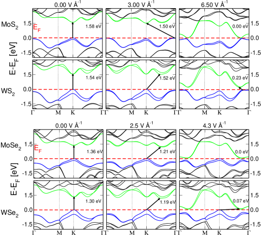
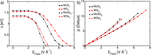
Fig. 2 shows the band gap and the dipole moment evolution of MoWSeS monolayers with respect to the field strength. The band gaps stay almost constant up to 3.5 and 2.0 V Å-1 for sulphides and selenides, respectively. At the same time the dipole moments increase linearly with external field strength, even in the regions where the band gaps are unaffected. Above a critical field strength, the decrease in the band gap is more rapid for the Mo-based systems compared with the W-counterparts. As the strength of the electric field increases, the polarization also increases and hence the dipole moment changes deviate from linearity, leading to the band gaps closure for critical electric fields.
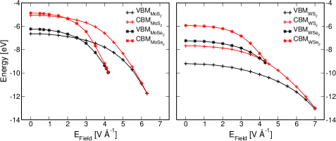
The changes in the energies of the valence band maximum (VBM) and CBM with the electric field are shown in Fig. 3. Slow reduction in the energy of both extrema are observed even for weak fields, however, above the critical values of electric field 2 V Å-1 (3.5 V Å-1) for selenides (sulphides), the change is more drastic.
The effective masses of electrons and holes at the point are very stable with respect to the external electric field (see Tab. 1). Also the band splitting caused by to the spin-orbit effect is not affected by the electric field. The presence of Stark effect, however, is pronounced and can be observed in the shape of the band structures (see Fig. 1).
| System | E | at point | ||
| (V Å-1) | (meV) | m/m0 | m/m0 | |
| 0.00 | 150 | 0.450 | -0.537 | |
| MoS2 | 3.00 | 150 | 0.451 | -0.546 |
| 4.00 | 149 | 0.451 | -0.551 | |
| 0.00 | 183 | 0.561 | -0.614 | |
| MoSe2 | 2.00 | 181 | 0.564 | -0.620 |
| 4.00 | 180 | 0.556 | -0.630 | |
| 0.00 | 430 | 0.367 | -0.334 | |
| WS2 | 3.00 | 424 | 0.381 | -0.342 |
| 4.00 | 415 | 0.393 | -0.347 | |
| 0.00 | 453 | 0.426 | -0.355 | |
| WSe2 | 2.00 | 443 | 0.435 | -0.360 |
| 4.00 | 441 | 0.455 | -0.372 | |
Applying external electric field causes changes especially in the conduction band and other minima, namely between the and , become close in energy to the CBM. Therefore, it might be of interest to investigate the electron effective masses for those minima (see Tab. 2). The effective masses of electron at those points are more sensitive to the external electric field than at the point and reduce (increase) significantly for the (). At zero fields, they are larger than the corresponding values at the point, though. Note, we do not report the hole effective masses for other maxima in the valence band (at the point), as the bands are very flat and the values become very large and meaningless.
| System | E | m/m0 | |
|---|---|---|---|
| (V Å-1) | CBM () | CBM () | |
| MoS2 | 0.00 | 0.956 | 0.599 |
| 3.00 | 0.676 | 1.259 | |
| MoSe2 | 0.00 | 0.776 | 0.5417 |
| 2.50 | 0.653 | 1.305 | |
| WS2 | 0.00 | 0.886 | 0.541 |
| 3.00 | 0.619 | 0.869 | |
| WS2 | 0.00 | 0.694 | 0.436 |
| 2.50 | 0.565 | 1.175 |
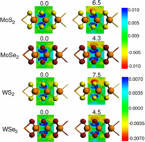
Fig. 4 shows the deformation density maps at zero and the critical electric field strengths. In these plots, the red zone refers to electron depletion, while the blue colour corresponds to an excess of electrons. In the equilibrium, there is a uniform charge distribution, symmetric with respect to the transition-metal layer for all MoWSeS monolayers. Once the electric field reaches a critical strength, that is at the point of semiconductor-metal transition, we observe a strong polarization of the system, indicated by the red colour that starts to dominate in the upper chalcogen layer, while the blue colour appears in the lower chalcogen layer. This means that a strong polarization occurs normal to the basal plane, inducing a dipole moment, which leads to the reduced band gaps.
In conclusion, we show that MoWSeS monolayers TX2, T = Mo, W, X = S, Se are very stable with respect to external electric fields that are common when applying a gate voltage. Only at very strong fields, exceeding 2 V Å-1, effects on the electronic structure become notable. Those include a Stark effect and the change of electronic structure, leading to a transition from direct to indirect band gap in the monolayers. Even though the band structures, in particular the conduction bands, change due to the Stark effect, quantities that dominate the electronic properties of the materials such as band gap, effective masses of electrons and holes, and the value of the spin-orbit splitting are unaffected by the external fields.
I Acknowledgements
Financial support by Deutsche Forschungsgemeinschaft (DFG, HE 3543/17-1) and the European Commission through the Initial Training Network (ITN) MoWSeS (GA FP7-PEOPLE-2012-ITN) and the Industrial Academic Partnership Pathways (IAPP) QUASINANO (GA FP7-PEOPLE-2009-IAPP) is acknowledged.
References
- Wang et al. (2012) Q. H. Wang, K. Kalantar-Zadeh, A. Kis, J. N. Coleman, and M. S. Strano, Nat. Nanotechnol., 7, 699 (2012).
- Mak et al. (2010) K. F. Mak, C. Lee, J. Hone, J. Shan, and T. F. Heinz, Phys. Rev. Lett., 105, 136805 (2010).
- Radisavljevic et al. (2011) B. Radisavljevic, A. Radenovic, J. Brivio, V. Giacometti, and A. Kis, Nat. Nanotechnol., 6, 147 (2011a).
- Coleman et al. (2011) J. N. Coleman, M. Lotya, A. O’Neill, S. D. Bergin, P. J. King, U. Khan, K. Young, A. Gaucher, S. De, R. J. Smith, I. V. Shvets, s. K. Arora, G. Stanton, H.-Y. Kim, K. Lee, G. T. Kim, G. S. Duesberg, T. Hallam, J. J. Boland, J. J. Wang, J. F. Do negan, J. C. Grunlan, G. Moriarty, A. Shmeliov, R. J. Nicholls, J. M. Perkins, E. M. Grieveson, K. Theuwissen, P. D. McComb, D W an d Nellist, and V. Nicolosi, Science, 331, 568 (2011).
- Radisavljevic et al. (2011) B. Radisavljevic, M. B. Whitwick, and A. Kis, Acs Nano, 5, 9934 (2011b).
- Radisavljevic et al. (2012) B. Radisavljevic, M. B. Whitwick, and A. Kis, Appl. Phys. Lett., 101, 043103 (2012).
- Lopez-Sanchez et al. (2013) O. Lopez-Sanchez, D. Lembke, M. Kayci, A. Radenovic, and A. Kis, Nat. Nanotechnol., 8, 497 (2013).
- Splendiani et al. (2010) A. Splendiani, L. Sun, Y. B. Zhang, T. S. Li, J. Kim, C. Y. Chim, G. Galli, and F. Wang, Nano Lett., 10, 1271 (2010).
- Kuc et al. (2011) A. Kuc, N. Zibouche, and T. Heine, Phys. Rev. B, 83, 245213 (2011).
- Sun et al. (2013) L. Sun, J. Yan, D. Zhan, L. Liu, H. Hu, H. Li, B. K. Tay, J.-L. Kuo, C.-C. Huang, D. W. Hewak, P. S. Lee, and Z. X. Shen, Phys. Rev. Lett., 111, 126801 (2013).
- Zhu et al. (2011) Z. Y. Zhu, Y. C. Cheng, and U. Schwingenschlögl, Phys. Rev. B, 84, 153402 (2011).
- Scalise et al. (2012) E. Scalise, M. Houssa, G. Pourtois, V. Afanas’ev, and A. Stesmans, Nano Research, 5, 43 (2012).
- Lu et al. (2012) P. Lu, X. Wu, W. Guo, and X. C. Z., Phys. Chem. Chem. Phys., 14, 13035 (2012).
- Johari and Shenoy (2012) P. Johari and V. B. Shenoy, ACS Nano, 6, 5449 (2012).
- Ghorbani-Asl et al. (2013) M. Ghorbani-Asl, S. Borini, A. Kuc, and T. Heine, Phys. Rev. B, 87, 235434 (2013a).
- Ghorbani-Asl et al. (2013) M. Ghorbani-Asl, N. Zibouche, M. Wahiduzzaman, A. F. Oliveira, A. Kuc, and T. Heine, Sci. Rep., 3, 2961 (2013b).
- Qi et al. (2013) J. Qi, X. Li, X. Qian, and J. Feng, Appl. Phys. Lett., 102 (2013).
- Yue et al. (2012) Q. Yue, S. Chang, J. Kang, X. Zhang, Z. Shao, S. Qin, and J. Li, Journal of Physics: Condensed Matter, 24 (2012).
- Ramasubramaniam et al. (2011) A. Ramasubramaniam, D. Naveh, and E. Towe, Phys. Rev. B, 84, 205325 (2011).
- Liu et al. (2012) Q. Liu, L. Li, Y. Li, Z. Gao, Z. Chen, and J. Lu, J. Phys. Chem. C, 116, 21556 (2012).
- Perdew et al. (1996) J. P. Perdew, K. Burke, and M. Ernzerhof, Phys. Rev. Lett., 77, 3865 (1996).
- te Velde and Baerends (1991) G. te Velde and E. J. Baerends, Phys. Rev. B, 44, 7888 (1991).
- Philipsen et al. (2012) P. H. T. Philipsen, G. te Velde, E. J. Bearends, J. Berger, P. L. de Boeij, J. Groenveld, E. S. Kadantsev, R. Klooster, F. Kootstra, P. Romaniello, D. G. Skachkov, J. G. Snijders, G. Wiesnekker, and T. Ziegler, “Band2012,” SCM, Theoretical Chemistry, Vrije Universiteit, Amsterdam, The Netherlands, http://www.scm.com (2012).
- Philipsen et al. (1997) P. H. T. Philipsen, E. van Lenthe, J. G. Snijders, and E. J. Baerends, Phys. Rev. B, 56, 13556 (1997).
- Zaharioudakis (2005) D. Zaharioudakis, Comput. Phys. Commun., 167, 85 (2005).