Intrinsic optical conductivity of modified-Dirac fermion systems
Abstract
We analytically calculate the intrinsic longitudinal and transverse optical conductivities of electronic systems which govern by a modified-Dirac fermion model Hamiltonian for materials beyond graphene such as monolayer MoS2 and ultrathin film of the topological insulator. We analyze the effect of a topological term in the Hamiltonian on the optical conductivity and transmittance. We show that the optical response enhances in the non-trivial phase of the ultrathin film of the topological insulator and the optical Hall conductivity changes sign at transition from trivial to non-trivial phases which has significant consequences on a circular polarization and optical absorption of the system.
pacs:
72.20-i, 78.67.-n, 78.20.-eI introduction
Two-dimensional (2D) materials have been one of the most interesting subjects in condensed matter physics for potential applications due to the wealth of unusual physical phenomena that occur when charge, spin and heat transport are confined to a 2D plane Xu . These materials can be mainly classified in different classes which can be prepared as a single atom thick layer namely, layered van der Waals materials, layered ionic solids, surface growth of monolayer materials, 2D topological insulator solids and finally 2D artificial systems and they exhibit novel correlated electronic phenomena ranging from high-temperature superconductivity, quantum valley or spin Hall effect to other enormously rich physics phenomena. two-dimensional materials can be mostly exfoliated into individual thin layers from stacks of strongly bonded layers with weak interlayer interaction and a famous example is graphene and hexagonal boron nitride Geim . The 2D exfoliates versions of transition metal dichalcogenides exhibit properties that are complementary to and distinct from those in graphene wang12 .
Optical spectroscopy is a broad field and useful to explore the electronic properties of solids. Optical properties can be tuned by varying the Fermi energy or the electronic band structure of 2D systems. Recently, developed 2D systems such as gapped graphene Neto09 , thin film of the topological insulator Hasan10 ; Tibook , and monolayer of transition metal dichalcogenides wang12 provide the electronic structures with direct band gap signatures. The optical response of semiconductors with direct band gap is strong and easy to explore experimentally since photons with energy greater than the energy gap can be absorbed or omitted. The thin film of the topological insulator, on the other hand, has been fabricated experimentally by using Sb2Te3 slab Zhang13 and has been shown that a direct band gap can be formed owing to the hybridization of top and bottom surface states. Furthermore, a non-trivial quantum spin Hall phase has been realized experimentally which was predicted previously in this system Lu10 ; Li10 ; HLi12 . Although pristine graphene and surface states of the topological insulator reveal massless Dirac fermion physics , by opening an energy gap they become formed as massive Dirac fermions. The thin film of the topological insulator and monolayer transition metal dichacogenides can be described by a modified-Dirac Hamiltonian. A monolayer of the molybdenum disulfide (ML-MoS2) is a direct band gap semiconductor Mak10 , however its multilayer and bulk show indirect band gap wang12 . This feature causes the optical response in ML-MoS2 to increases in comparison with its bulk and multilayer structures cao12 ; cui12 ; mak12 ; mak13 ; wu13 .
One of the main properties of ML-MoS2 is a circular dichroism aspect responding to a circular polarized light where the left or right handed polarization of the light couples only to the or valley and it provides an opportunity to induce a valley polarized excitation which can profoundly be of interest in the application for valleytronics Rycerz07 ; xiao07 ; yao08 . Another peculiarity of ML-MoS2 is the coupled spin-valley in the electronic structure which is owing to the strong spin-orbit coupling originating from the existence of a heavy transition metal in the lattice structure and the broken inversion symmetry too. xiao12 These two aspects are captured in a minima massive Dirac-like Hamiltonian introduced by Xiao et al. xiao12 However it has been shown , based on the tight-binding Rostami13 ; Liu13 and method Kormanyos13 , that other terms like an effective mass asymmetry, a trigonal warping, and a diagonal quadratic term might be included in the massive Dirac-like Hamiltonian. The effect of the diagonal quadratic term is very important, for instance, if the system is exposed by a perpendicular magnetic field, it will induce a valley degeneracy breaking term Rostami13 . The optical properties of ML-MoS2 have been evaluated by ab-initio calculations Carvalho13 and studied theoretically based on the simplified massive Dirac-like model Hamiltonian Li12 , which is by itself valid only near the main absorbtion edge. A part of the model Hamiltonian which describes the dynamic of massive Dirac fermions are known in graphene committee to have an optical response quite different from that of a standard 2D electron gas. Thus it would be worthwhile to generalize the optical properties of such systems by using the modified-Dirac fermion model Hamiltonian.
The modified Hamiltonian for ML-MoS2 without trigonal warping effect at point is very similar to the modified-Dirac equation which has been studied for an ultrathin film of the topological insulator (UTF-TI) around point. Lu10 ; Shan10 The modified-Dirac Hamiltonian reveals non-trivial quantum spin hall (QSH) and trivial phases corresponding to the existence and absence of the edge states, respectively. Those phases have been predicted theoretically Lu10 ; Li10 ; HLi12 ; Kim12 and recently observed by experiment Zhang13 . An enhancement of the optical response of UTF-TI has been obtained in the non-trivial phase peres13 and a band crossing is observed in the presence of the structure inversion asymmetry induced by substrate Lu13 . Since the modified-Dirac Hamiltonian incorporates an energy gap and a quadratic term in momentum which both have topological meaning, it is natural to expect that the topological term of the Hamiltonian plays an important role in the optical conductivity. In this paper, we analytically calculate the intrinsic longitudinal and transverse optical conductivities of the modified-Dirac Hamiltonian as a function of photon energy. This model Hamiltonian covers the main physical properties of ML-MoS2 and UTF-TI systems in the regime where interband transition plays a main role. We analyze the effect of the topological term in the Hamiltonian on the optical conductivity and transmittance. Furthermore, we show that the UTF-TI system has a non-trivial phase and its optical response enhances in addition, the optical Hall conductivity changes sign at a phase boundary, when the energy gap is zero. This changing of the sign has a significant consequence on the circular polarization and the optical absorbtion of the system.
The paper is organized as follows. We introduce the low-energy model Hamiltonian of ML-MoS2 and UTF-TI systems and then the dynamical conductivity is calculated analytically by using Kubo formula in Sec. II. The numerical results for the optical Hall and longitudinal conductivities and optical transmittance are reported and we also provide discussions with circular dichroism in both systems in Sec. III. A brief summary of results is given in Sec. IV.
II theory and method
The low-energy properties of the ML-MoS2 and other transition metal dicalcogenide materials can be described by a modified-Dirac equation Rostami13 ; Kormanyos13 ; Liu13 and the Hamiltonian around the and points is given by
where the Pauli matrices stand for a pseudospin which indicates the conduction and valence band degrees of freedom, denotes the two independent valleys in the first Brillouin zone, and . The numerical values of the parameters will be given in the Sec. III.
The UTF-TI system, on the other hand, can be described by a modified Dirac Hamiltonian around the point with two independent hyperbola (isospin) degree of freedoms Lu10 ; Shan10 and thus the Hamiltonian reads
| (2) |
Note that the Pauli matrices in this Hamiltonian stand for the real spin where spin is rotated by operator which results in and and the isospin index of indicates two independent solutions of UTF-TI which are degenerated in the absence of the structure inversion asymmetry and can be assumed as an internal isospin (spin, valley, or sublattice) degree of freedom. Two mentioned models, Eqs. (II) and (2), are similar to some extent and describe similar physical properties.
Generally, the Hamiltonian around the and ) points for UTF-TI and monolayer MoS2 systems, respectively can be re-written as
| (3) |
where for UTF-TI and for ML-MoS2. Note that , and we set . The eigenvalue and eigenvector of the Hamiltonian, Eq. (3) can be obtained as
| (4) |
and velocity operators along the and directions are
| (5) |
The intrinsic optical conductivity can be calculated by using the Kubo formula Stauber08 ; Tse11 ; Louie06 in a clean sample and it is given by
| (6) |
where is the Fermi distribution function. We include only the interband transitions and the contribution of the intraband transitions, which leads to the fact that the Drude-like term, is no longer relevant in this study since the momentum relaxation time is assumed to be infinite. This approximation is valid at low-temperature and a clean sample where defect, impurity, and phonon scattering mechanisms are ignorable. We also do not consider the bound state of exciton in the systems. After straightforward calculations (details can be found in Appendix A), the real and imaginary parts of diagonal and off-diagonal components of the conductivity tensor at are given by
| (7) |
where and refer to the real and imaginary parts of and denotes the principle value. It is worthwhile mentioning that the conductivity for ML-MoS2 for can be found by implementing and . Using these transformations, the velocity matrix elements around the point can be calculated by taking the complex conjugation of the corresponding results for the case. Furthermore, for the UTF-TI case system, we must replace and by their opposite signs which lead to the same results in comparison with the ML-MoS2 case around point. More details in this regard are given in Appendix A.
II.1 Optical conductivity of ML-MoS2
Having obtained the general expressions of the conductivity for the modified-Dirac fermion systems, the conductivity of two examples namely the ML-MoS2 and UTF-TI could be obtained. Here, we would like to focus on the ML-MoS2 case and explore its optical properties, although all results can be generalized to the UTF-TI system as well. Therefore, the optical conductivity for each spin and valley components of ML-MoS2 can be obtained by using appropriate substitution in Eq. (II) and results are written as
where , , , , and .
Note that in the case of UTF-TI, there is no extra spin index of as a degree of freedom and might be replaced by , consequently we have and rather than and . To be more precise, , which is located out of the radical in Eq. (II.1), might be replaced by in the to achieve desirable results corresponding to the UTF-TI. It is clear that the dynamical charge Hall conductivity vanishes in both the UTF-TI and ML-MoS2 systems due to the presence of the time reversal symmetry. For the MoS2 case, the spin and valley transverse ac-conductivity are given by
| (9) |
and for the longitudinal ac-conductivity case, an electric field can only induce a charge current and corresponding conductivity is given as
| (10) |
Moreover, the longitudinal conductivity is the same as expression given by Eq. (10) for the UTF-TI case however, the Hall conductivity is slightly changed. Owing to the coupling between the isospin and the spin indexes, the hyperbola Hall conductivity is a spin Hall conductivity Lu10 ; Zhang13 and it is thus given by
| (11) |
II.2 Intrinsic dc-conductivity
To find the static conductivity in a clean sample, we set and thus the interband longitudinal conductivity vanishes. Consequently, we calculate only the transverse conductivity in this case. At zero temperature, the Fermi distribution function is given by a step function, i. e. . We derive the optical conductivities for the case of ML-MoS2 and results corresponding to the UTF-TI can be deduced from those after appropriate substitutions. Most of the interesting transport properties of ML-MoS2 originates from its spin splitting band structure for the hole doped case. Therefore, for the later case, when the upper spin-split band contributes to the Fermi level state, the dc-conductivity is given by
| (12) |
and for the spin-down component we thus have
| (13) | |||||
where is the ultra violate cutoff and stands for the chemical potential and it is easy to show that at large cutoff values. In a precise definition, terms are the Chern numbers for each spin and valley degrees of freedom and the total Chern number is zero owing to the time reversal symmetry. Intriguingly, the quadratic term in Eq. (3), , leads to a new topological characteristic. When , with , system has a trivial phase with no edge mode closing the energy gap however for the case that , the topological phase of the system is a non-trivial with edge modes closing the energy gap. In the case of the ML-MoS2, the tight binding model Rostami13 ; Gomez13 predicts the trivial phase ( with . However, a non-trivial phase is expected by Refs. [Kormanyos13, , Liu13, ] (where ) which leads to . In other words, the term proportional to has a topological meaning in Z2 symmetry invariant like the UTF-TI system Lu10 and the sign of plays important role.
The transverse intrinsic dc-conductivity for the hole doped ML-MoS2 case, is given by
| (14) |
where, at large cutoff, stands for the valley Chern number and it equals to zero or corresponding to the non-trivial or trivial band structure, respectively. In the case of the UTF-TI, the isospin Hall conductivity is
| (15) |
where and at large cutoff. This result is consistent with that result obtained by Lu et al. Lu10 . It should be noted that in the absence of the diagonal quadratic term, the non-zero valley Chern number at zero doping predicts a valley Hall conductivity, which is proportional to . Therefore, the exitance of edge states , which can carry the valley current, is anticipated. However, Z2 symmetry prevents the edge modes from existing. Since the Z2 topological invariant is zero when the gap is caused only the inversion symmetry breaking yao09 , thus the topology of the band structure is trivial and there are no edge states to carry the valley current when the chemical potential is located inside the energy gap. Therefore, we can ignore the valley Chern number in and thus the results are consistent with those results reported by Xiao el al. xiao12 at a low doping rate where .
II.3 Intrinsic dynamical conductivity
In this section, we analytically calculate the dynamical conductivity of the modified-Dirac Hamiltonian which results in the trivial and non-trivial phases. Using the two-band Hamiltonian, including the quadratic term in momentum, the optical Hall conductivity for each spin and valley components are given by
| (16) | |||||
where and indicate to the real and imaginary parts, respectively and reads as below (details are given in Appendix B)
| (17) |
where , , , and . The value of can be evaluated from . Note that , the ultra violate cutoff, is assumed to be equal to . Some special attentions might be taken for the situation in which there is no intersection between the Fermi energy and the band energy, for instance in a low doping hole case of the ML-MoS2 in which the Fermi energy lies in the spin-orbit splitting interval. In this case, the Fermi wave vector (, which has no contribution to the Fermi level) vanishes.
The quadratic terms can also affect profoundly on the longitudinal dynamical conductivity which plays main role in the optical response when the time reversal symmetry is preserved. In this case, one can find
| (18) |
where is given by (details are given in Appendix B)
| (19) | |||||
It is worthwhile mentioning that the and functions do not depend on the term given in Eq. (3). For in Eq. (3), we have , , therefore reduces to and in a similar way, reduces to . Here and read as below
Using Eqs. (II.1) and (II.3), the conductivity simplifies when and the results are
| (21) | |||||
The longitudinal conductivity for the case of is given by the following relations for the electron doped case
| (22) |
These relations are consistent with those results reported in Ref. [Li12, ]. Furthermore, dropping the term gives rise to the optical conductivity of gapped graphene and the result is in good agreement with the universal conductivity of graphene Zigler07 for .
III numerical results
In most numerical results, we use where and . These values have been obtained in Ref. [Rostami13, ]. Moreover, for the sake of completeness, we introduce two other sets of the parameters as and another set corresponding to the same effective masses ( for ) for electron and hole bands. These parameters are calculated by using the procedure reported in Ref. [Rostami13, ]. The later comparison helps us to perceive the validity of the effective mass approximation for the ML-MoS2 system and for this purpose, we assume the same effective masses for electron and hole bands to compare the spin Hall conductivity resulted from the Dirac-like and modified-Dirac Hamiltonians. Notice that all energies are measured from the center of the energy gap.
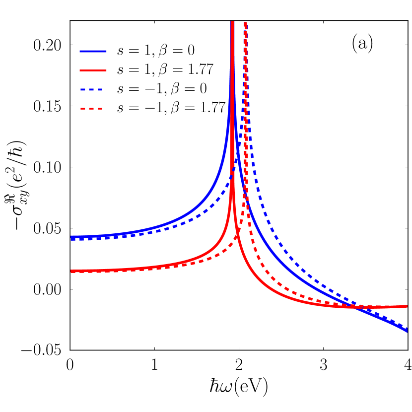
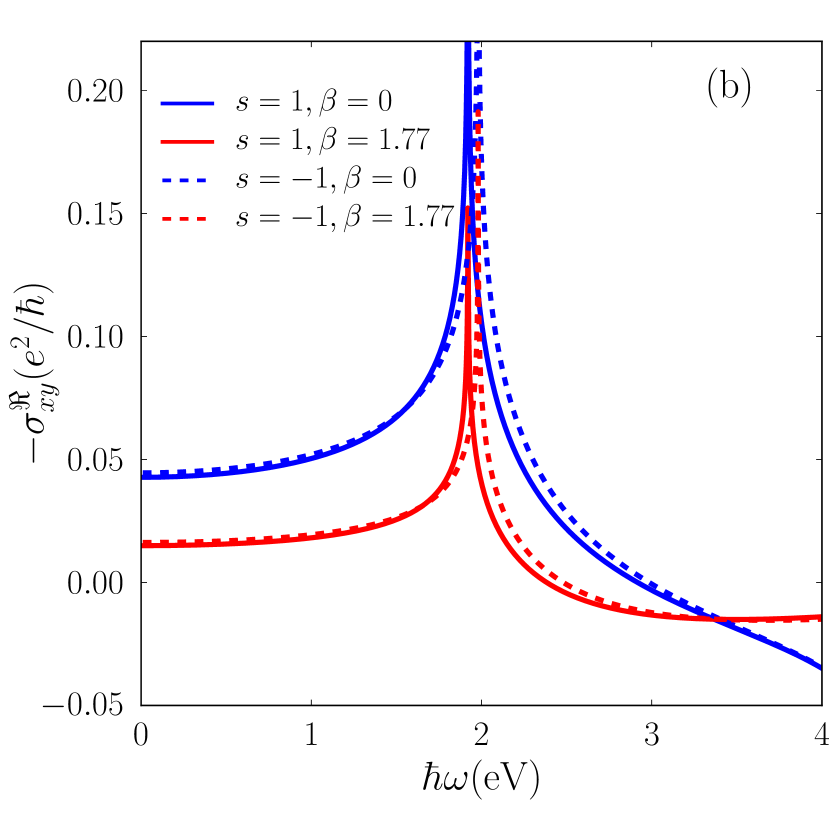
The real part of the optical Hall and longitudinal conductivities for the two set of parameters, with and without quadratic terms, are illustrated in Fig. 1 and Fig. 2 where top and bottom panels indicate electron and hole doped systems, respectively. The effect of the mass asymmetry between the effective masses of the electron and hole () bands is neglected and it will be discussed later. It is clear that the quadratic term, , causes a reduction of the intensity of the optical Hall conductivity with no changing of the position of peaks for both electron and hole doped cases. The position of peaks in the real part of Hall conductivity is given by for case and for each spin component with corresponding Fermi wave vector and for the case that . Surprisingly, the last two equations for the later case are simultaneously fulfilled the equation in frequency. In the energy range shown in the figures, the numerical value of the peak position for both cases are approximately equal and it indicates that the position of peaks and steplike configuration don’t change due to the term in a certain Fermi energy. It should be noticed that the intensity of the real part of decreases with the quadratic term. Consequently, it indicates that the effective mass approximation of the Hamiltonian for the ML-MoS2 is not completely valid because two sets of parameters with the same effective masses are showing distinct results.
III.1 Mass asymmetry between electron and hole
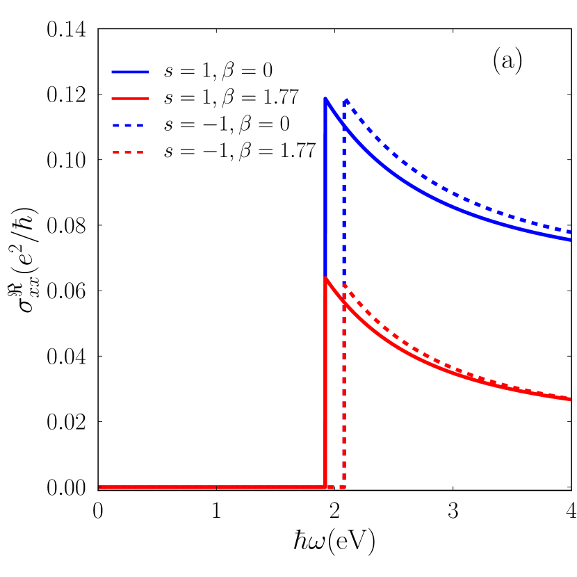
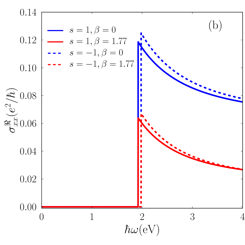
In this subsection, we consider the mass asymmetry between electron and hole bands and then the conductivity of the ML-MoS2 is calculated for the Hamiltonian given in Eq. (3). The results are illustrated in Figs. 3 and 4 around the point. Due to the mass asymmetry, a small splitting between electron and hole doped cases takes place in the spin-up component. On the other hand, there is considerable splitting between electron and hole doped cases due to both spin-orbit coupling and mass asymmetry for the spin-down case. We also note a sharp onset in the imaginary part of the conductivity, minimum energy associated with the possible interband optical transition. Moreover, corresponding to the onset in where there is a peak in its real (imaginary) part at the same energy as they are related by the Kramers-Kroning relations.

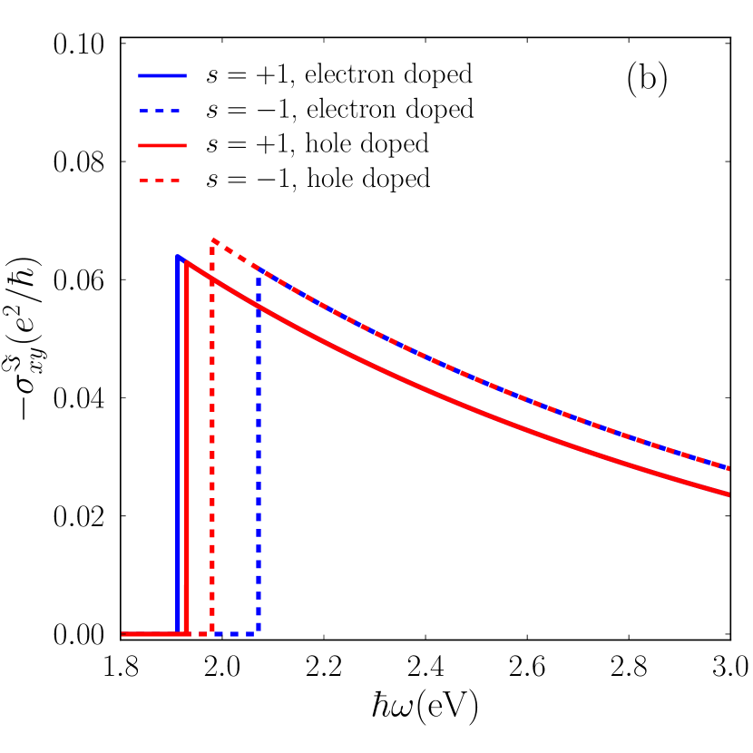
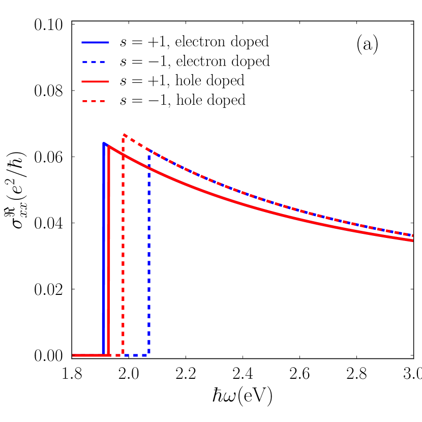
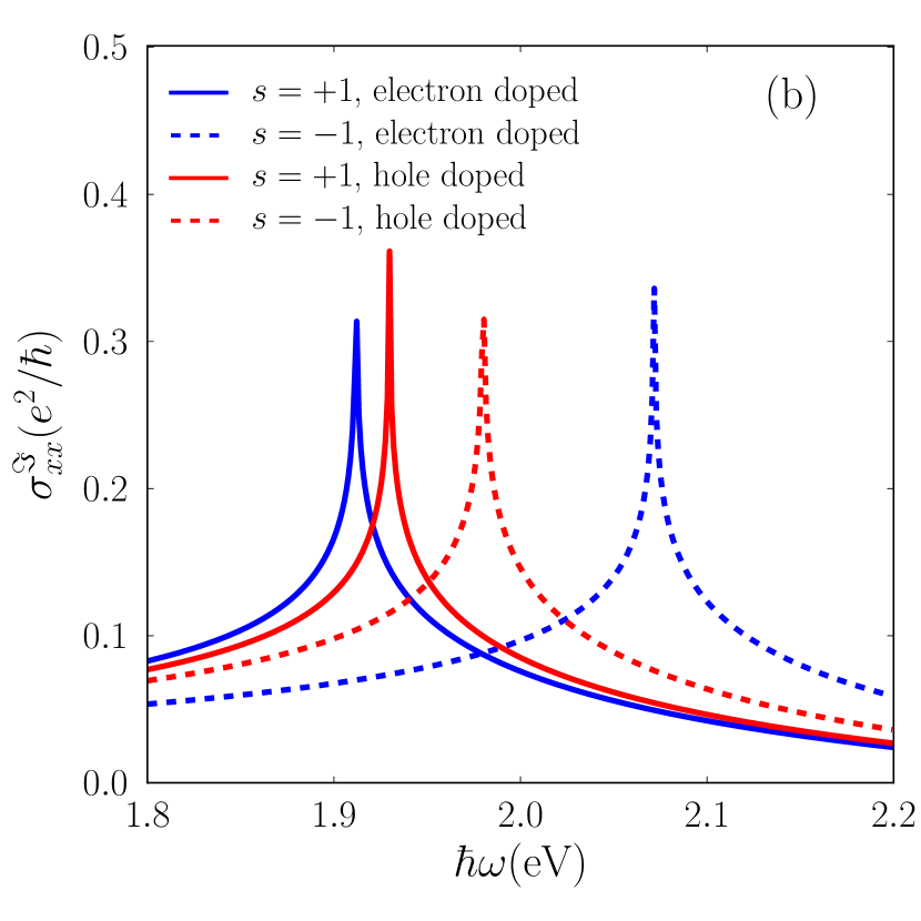
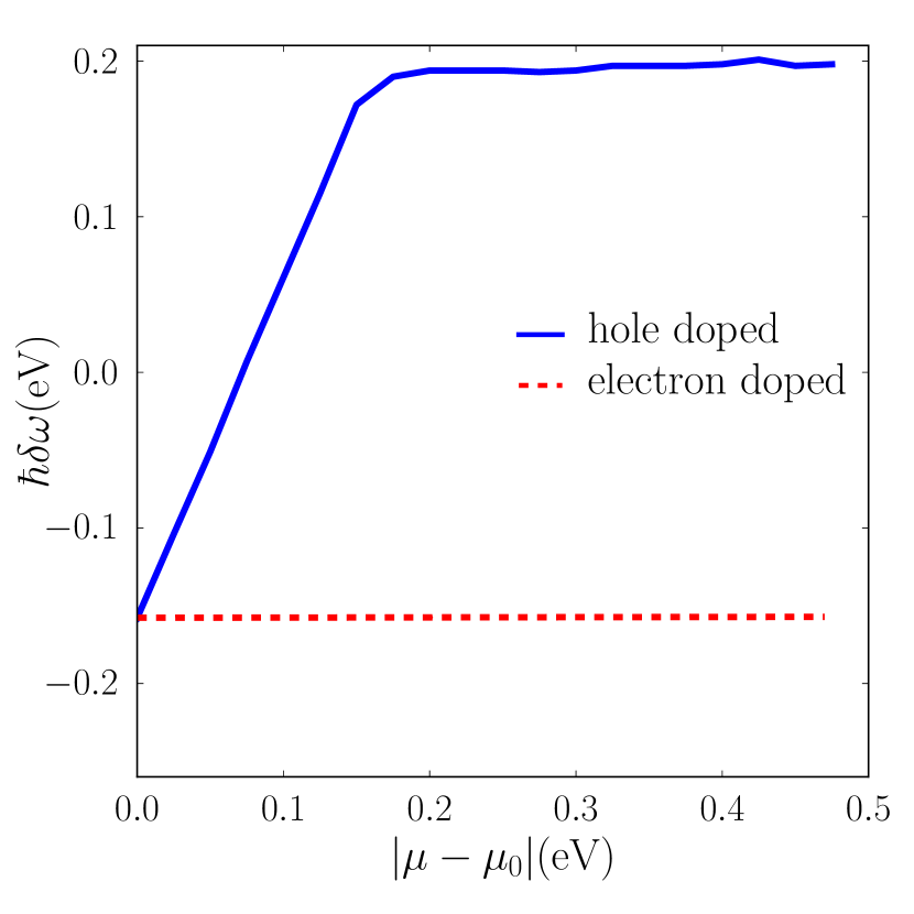
The position of peaks or steplike configuration of the dynamical conductivity, can be controlled by the doping rate. Figure. 5 shows the difference between the position of those peaks, , around the point for electron and hole doped cases corresponding to the real part of the Hall conductivity for each spin component. As it is clearly shown in this figure, increases linearly from a negative value to a positive one up to a saturation value ( for the hole doped case. The linear part of the result originates from the spin splitting in the valence band and the fact that there is two fermi wave vectors in which one component spin has zero Fermi wave vector and does not change by increasing the doping rate. Finally, by increasing the Fermi energy, two Fermi wave vectors contribute to the calculations and the position of both peaks move in the same way and lead to a saturation value for .
III.2 Circular dichroism and Optical transmittance
One of the main optical properties of the monolayer transition metal dichalcogenide system is the circular dichroism when it is exposed by a circularly polarized light in which left- or right-handed light can be absorbed only by or valley and it makes the material promising for the valleytronic field. This effect originates from the broken inversion symmetry and it can be understood by calculating the interband optical selection rule for incident right-(+) and left-(-)handed light. The photoluminescence probability for the modified Dirac fermion Hamiltonian is
| (23) |
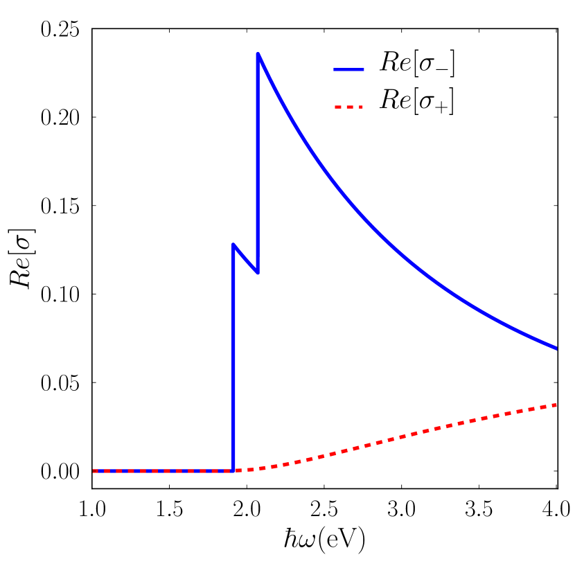
where . Notice that the mass asymmetry term, , has no effect on the optical selection rule. The selection rule can simply prove the circular dichroism in the ML-MoS2. Another approach which helps us to understand this effect is to calculate the optical conductivity around the point of two kinds of light polarizations as which has been calculated by using the Dirac-like model yao08 ; Li12 and now, we modify that by using the modified-Dirac Hamiltonian. Figure. 6 shows the coupling of the light and valleys. Note that is large and comparable in size for either spin up or down while is small in comparison. The valley around the point can couple only to the left-handed light and this effect is washed up by increasing the frequency of the light and the result is in good agreement with recent experimental measurements mak12 .
Furthermore, the optical transmittance is an important physical quantity and it can be evaluated stemming from the conductivity. The optical transmittance of a free standing thin film exposed by a linear polarized light is given by Ferreira11
| (24) |
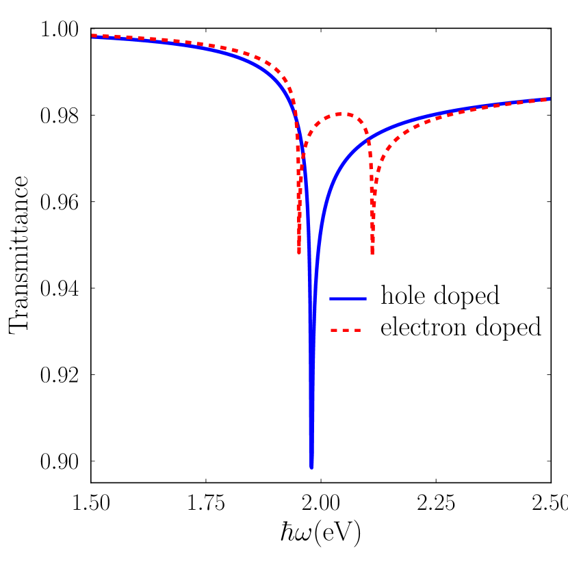
where and are the vacuum impedance and the optical conductivity of the thin film, respectively. For the ML-MoS2 case, the total Hall conductivity in the presence of the time reversal symmetry is zero and the total longitudinal conductivity is given by . The optical transmittance of the multilayer of MoS2 systems has been recently measured Gomez13 and it is about for each layer in the optical frequency range. The optical transmittance of the ML-MoS2 is displayed in Fig. 7 for both electron and hole doped cases using the numerical value defined as . The result shows that the optical transmittance is about for the frequency range in which both spin components are active for giving response to the incident light. Importantly, for the electron dope case, there are two minimums with distance about in frequency which mostly indicates the spin-orbit splitting () in the valence band and it is consistent with the results illustrated in Fig. 5. The optical transmittance for electron doped case is about in all frequency range. Moreover, for the hole dope case as it is shown in Fig. 5, the optical transmittance changes by tuning doping rate. Interestingly, at eV the difference between the position of peaks of two spin components, is approximately zero. Consequently, the total optical conductivity enhances in this resonating doping rate which has significant effect on the optical transmittance of the system where the transmittance decreases and particularly reaches to a value less than at the resonance frequency when . Our numerical calculations show that the hole doped ML-MoS2 is darker than the electron doped one specially close to the resonance frequency. Furthermore, this feature provides an opportunity with measuring the spin-orbit coupling by an optical transmittance measurement.
III.3 Optical response in the non-trivial phase
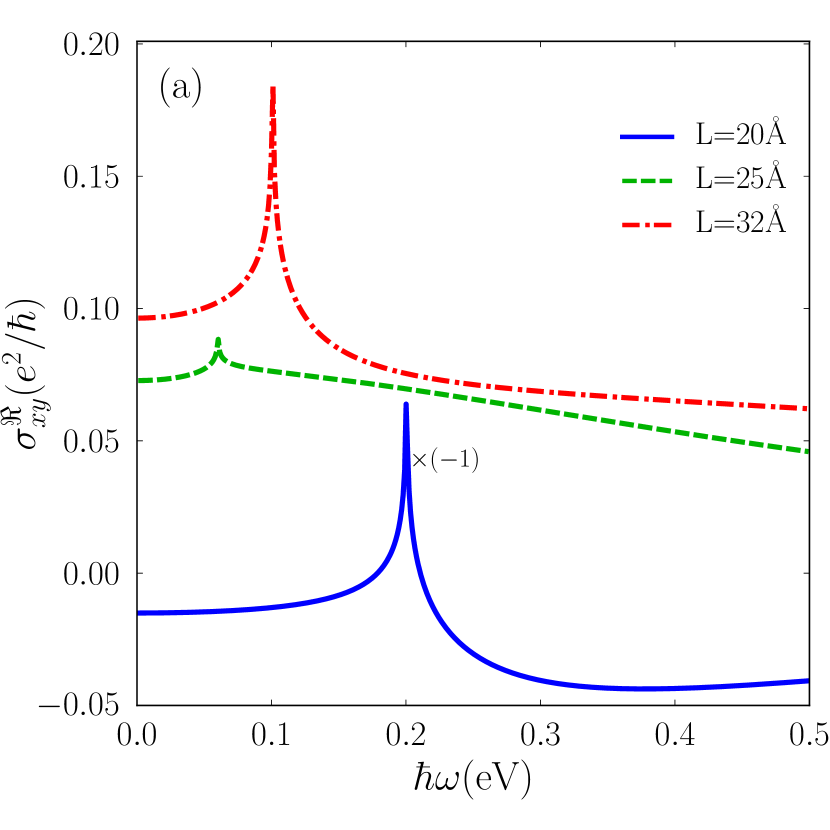
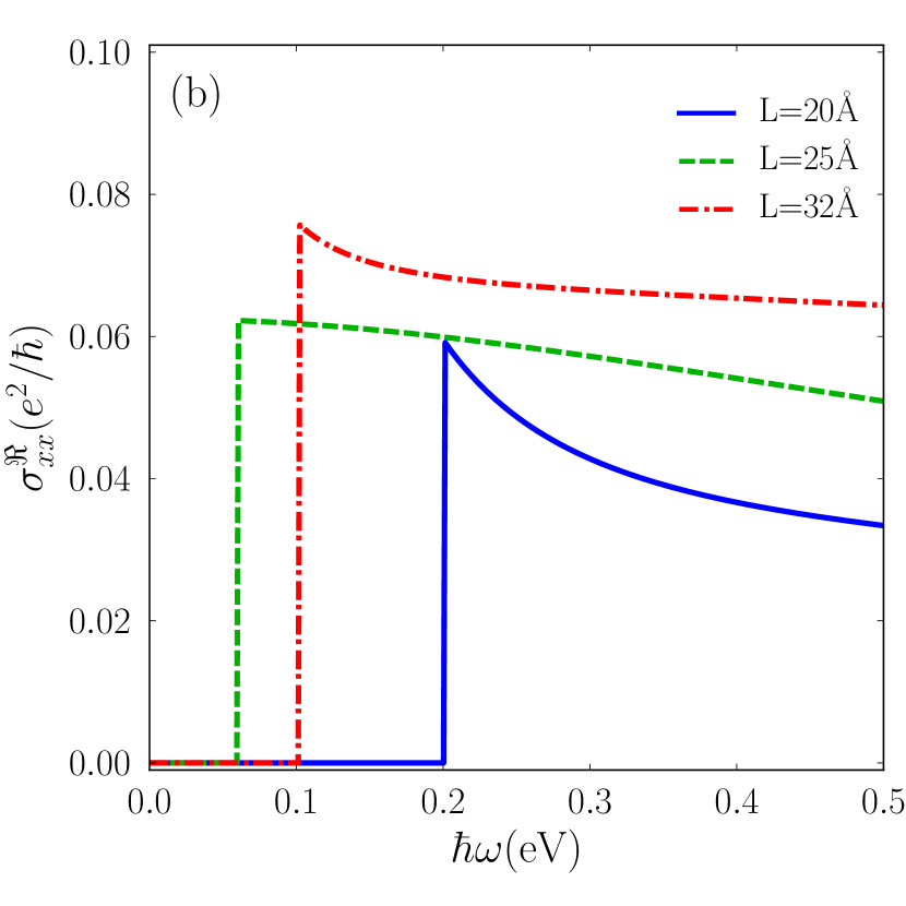
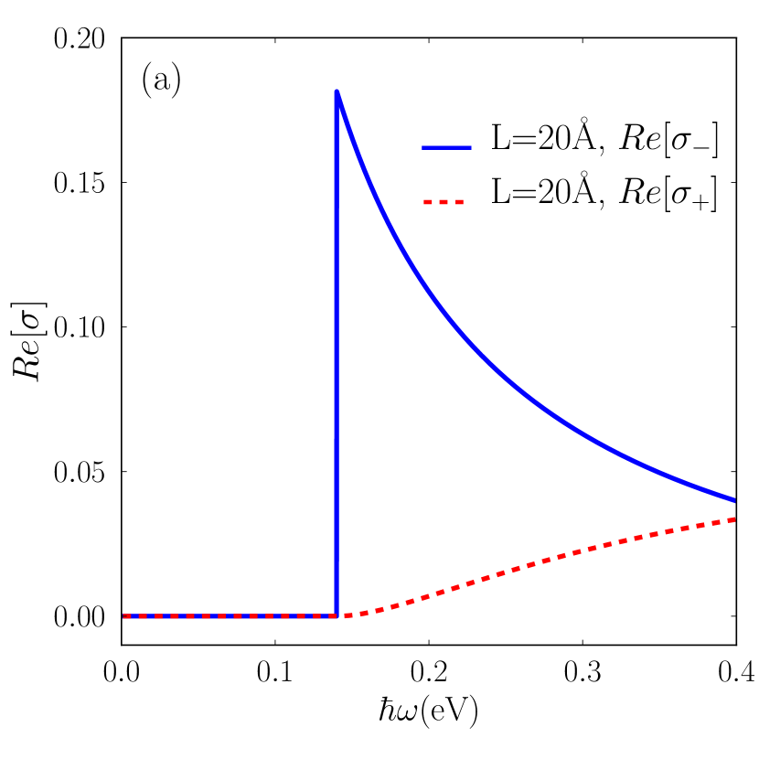
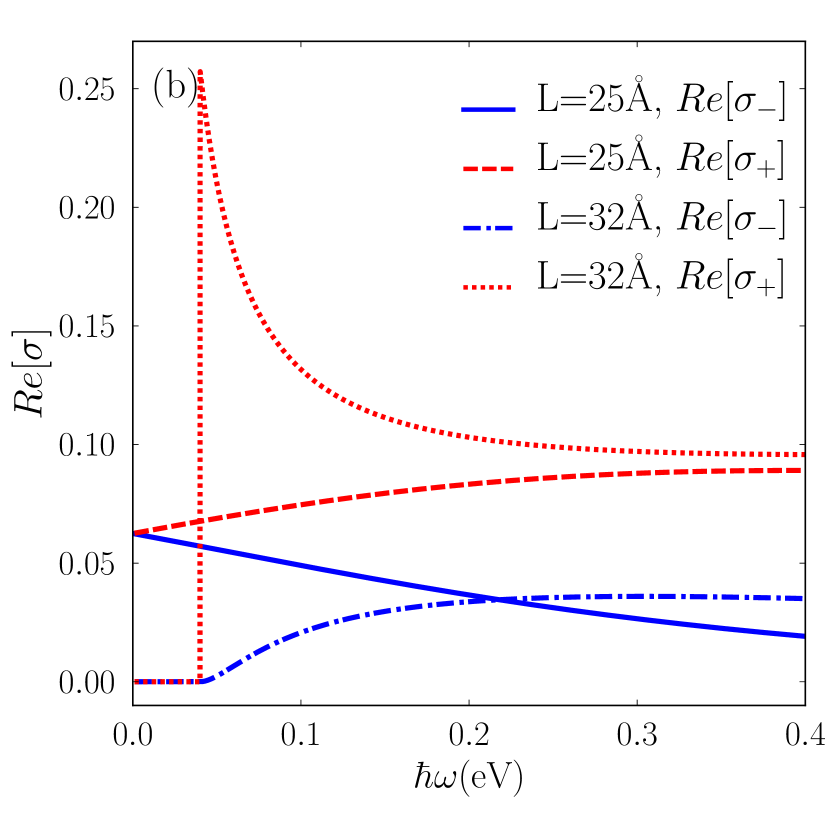
The modified-Dirac Hamiltonian shows a non-trivial phase when and it has been numerically shown that in this phase a light matter interaction enhances due to the change of the parabolic band dispersion into the shape of a Mexican-hat with two extrema peres13 . To fulfill such a band dispersion, a negative value with a large absolute value is required and it is accessible for an ultrathin film of the topological insulator. The sign and the absolute values of the parameters can be manipulated by the thickness of the thin film, while in the case of the ML-MoS2, to the best of our knowledge, it is barely possible to create a Mexican hat like dispersion relation even for the model Hamiltonian with a non-trivial topology phase Kormanyos13 ; Liu13 . In this case, we plot the optical Hall and longitudinal conductivities of the UTF-TI in its trivial and non-trivial phases. In the UTF-TI zhang09 system, in which only in-plan components of momentum are relevant, one can find the Hamiltonian given by Eq. (2) where the numerical value of the model parameters depends on the thickness of the thin films Lu10 ; Shan10 . We consider three different thicknesses for which three sets of parameters Lu10 are listed in Table I. We also neglect the value of which is just a constant shift in the energy.
| L(Å) | (eV) | (eV) | ||
|---|---|---|---|---|
| 20 | 0.14 | -2.22 | -1.05 | 23.67 |
| 25 | 0.0 | -2.21 | -2.37 | 18.41 |
| 32 | -0.04 | -2.20 | -3.94 | 6.31 |
As it can be seen from table I, a sample with or indicates the trivial or non-trivial phases, respectively. However for a sample with the energy gap vanishes and thus at critical thickness, , the trivial to non-trivial phase transition takes place. Hereafter, we call that a phase boundary.
Now, we calculate the real part of the Hall and longitudinal conductivities for and the results are illustrated in Fig. 8. It shows that the conductivity enhances in the non-trivial phase which is consistent with previous numerical work. peres13 More interestingly, we are now showing that the Hall conductivity changes sign through changing the thickness and it is very important in the circular dichroism effect. This changing of the sign means a different helicity of the light can be coupled to the system. It is worth mentioning that the circular dichroism effect on the electronic system governing modified-Dirac Hamiltonian is also possible when energy gap is zero yao08 ; Li12 . The selection rule equation reads as for the case of zero gap. This expression indicates that the circular polarization is achievable away from the point even in the absence of the energy gap. It might be emphasized that the peak in the optical conductivity at zero energy gap originates from a non-zero Fermi energy in which the low energy part of phase space is no longer available for a photon absorbtion process jahn based on the Pauli exclusion principle. More precisely, there is a peak at energy point in the topological insulator case and it can be seen from Eqs. (II.3) and (II.3). Therefore, the peak disappears at zero Fermi energy for a gapless system. In Fig. 9, we show the optical conductivity for the two helicities of light for . The results show that the circular polarization changes sign for negative value of the gap and it gets more strength in the non-trivial phase rather than the trivial phase.
IV summary
We have analytically calculated the intrinsic conductivity of the electronic systems which govern a modified-Dirac Hamiltonian by using the Kubo formula. We have studied the effect of the quadratic term in momentum, , which has been recently predicted, and found the different optical responses. This discrepancy originates from the different topological structures of the systems. Our calculations show that the -term has no effect on the position of the peak of the optical conductivity but it has considerable effect on its magnitude. Therefore, it shows that the same effective mass approximation for electron and hole bands for monolayer MoS2 can not fully describe the optical properties. The effect of the strong spin-orbit interaction can be traced by the difference of the energy interval between the position of the peak in the optical conductivity for the two spin components in electron and hole doped cases. We have shown that this interval for the electron doped case is approximately constant while for the hole doped case, it increases from a negative value to a positive one, and then it increases linearly up to a saturation value. The effect of the mass asymmetry in monolayer MoS2 induces a small splitting between the conductivity spectrum for the electron and hole doped cases. The circular dichroism effect is investigated for the modified-Dirac Hamiltonian of the monolayer MoS2 by calculating the selection rule and the optical conductivity. We have also obtained the optical transmittance of the monolayer MoS2 for the hole and electron doped cases and the results show that the valence band spin splitting has considerable effect on the intensity of the transmittance.
We have also studied the effect of the quantum phase transition, which occurs owing to the reducing of the thickness, on the optical conductivity of the thin film of the topological insulator. We have shown that at the phase boundary, when the energy gap is zero, the diagonal quadratic term plays a significant role on the optical conductivity and selection rule. Moreover, we have illustrated that the optical response enhances and the optical Hall conductivity changes sign in the non-trivial phase (QSH) and the phase boundary.
Acknowledgements.
R. A. would like to thank the Institute for Material Research in Tohoku University for its hospitality during the period when the last part of this work was carried out.Appendix A
In this appendix, the details of the calculations deriving Eq. (II.1) are presented. Since , we get
| (A.1) |
owing to the fact that the mass asymmetry parameter plays no role in the velocity matrix elements. Using we have
| (A.2) |
In this case
| (A.3) |
Consequently, the product of the velocity matrix elements are
| (A.4) |
Using , one can find
| (A.5) |
After substituting Eq. (A) into Eq. (A), we get
Using , one can find
Using where stands for principal value, it is easy to show that the real and imaginary parts of diagonal and off-diagonal components of the conductivity tensor read as below
| (A.8) |
To find the conductivity around point we must implement the following changes: and . Using these transformations, the velocity matrix elements around the point can be calculated by taking complex conjugation of the corresponding results around the point. Moreover, according to the following dimensionless parameters, , and thus for positive frequency in absorbtion process. Thus Eq. (II.1) for the dynamical transverse and longitudinal conductivity is obtained.
Appendix B
In this appendix, the details of calculations for some integrals which appear in our model are presented. Using new variables and , it is easy to show that and we have
| (B.1) | |||||
where , and are given by
| (B.2) |
and can be calculated by defining as a new variable where and it leads to
| (B.3) | |||||
By defining , and are obtained as
| (B.4) |
Using the above expressions for , and , it is easy to prove Eqs. (II.3) and (19).
References
- (1) M. Xu, T. Liang, M. Shi, and H. Chen, Chemical Reviwes, 113, 3766 (2013).
- (2) A. K. Geim, and I. V. Grigorrieva, Nature (London) 499, 419 (2013).
- (3) Q. H. Wang, K. Kalantar-Zadeh, A. Kis, J. N. Coleman, and M. S. Strano, Nat. Nanotechnol. 7, 699 (2012).
- (4) A. H. Castro Neto, F. Guinea, N. M. R. Peres, K. S. Novoselov and A. K. Geim, Rev. Mod. Phys. 81, 109 (2009).
- (5) M. Z. Hasan, C. L. Kane, Rev. Mod. Phys. 82, 3045 (2010).
- (6) Shun-Qing Shen,Topological insulator: Dirac equation in condesed matters, Springer (2012).
- (7) T. Zhang, J. Ha, N. Levy, Y. Kuk, and J. Stroscio, Phys. Rev. Lett. 111, 056803 (2013).
- (8) H.-Z. Lu, W.-Y. Shan, W. Yao, Q. Niu, and S.-Q. Shen, Phys. Rev. B 81, 115407(2010).
- (9) H. Li, L. Sheng, D. N. Sheng, and D. Y. Xing, Phys. Rev. B 82, 165104 (2010).
- (10) H. Li, L. Sheng, and D. Y. Xing, Phys. Rev. B 85, 045118(2012).
- (11) K. F. Mak, C. Lee, J. Hone, J. Shan, and T. F.Heinz, Phys. Rev. Lett. 105, 136805 (2010).
- (12) K. F. Mak, K. He, J. Shan, and T. F. Heinz, Nat. Nanotechnol. 7, 494 (2012).
- (13) K. F. Mak, K. He, C. Lee, G. H. Lee, J. Hone, T. F. Heinz, and J. Shan, Nat. Mat. 12, 207 (2013).
- (14) H. Zeng, J. Dai, W. Yao, D. Xiao, and X. Cui, Nat. Nanotechnol. 7, 490 (2012).
- (15) T. Cao, G. Wang, W. Han, H. Ye, C. Zhu, J. Shi, Q. Niu, P. Tan, E. Wang, B. Liu, and J. Feng, Nature Commun. 3, 887 (2012).
- (16) S. Wu, J. S. Ross, G. B. Liu, G. Aivazian, A. Jones, Z. Fei, W. Zhu, D. Xiao, W. Yao, D. Cobden, and X. Xu, Nat. Phys. 9, 149 (2013).
- (17) A.Rycerz, J.Tworzydlo, and C. W. J. Beenakker, Nat. Phys. 3, 172 (2007).
- (18) D.Xiao, W.Yao, and Q. Niu, Phys. Rev. Lett. 99, 236809 (2007).
- (19) W.Yao, D. Xiao, and Q. Niu, Phys. Rev. B 77, 235406 (2008).
- (20) Di Xiao, Gui-Bin Liu, W. Feng, X. Xu, and W. Yao, Phys. Rev. Lett. 108, 196802 (2012).
- (21) H. Rostami, A. G. Moghaddam, and R. Asgari, Phys. Rev. B 88, 085440 (2013).
- (22) G. -B. Liu, W. -Y. Shan, Y. Yao, W. Yao, D. Xiao, Phys. Rev. B 88, 085433 (2013).
- (23) A. Kormanyos, V. Zolyomi, N. D. Drummond, P. Rakyta, G. Burkard, and V. I. Fal’ko, Phys. Rev. B 88, 045416 (2013).
- (24) A. Carvalho, R. M. Ribeiro, and A. H. Castro Neto, Phys. Rev. B 88, 115205 (2013).
- (25) Zhou Li and J. P. Carbotte, Phys. Rev. B 86, 205425(2012).
- (26) W.-Y. Shan, H.-Z. Lu, and S.-Q. Shen, New J. Phys. 12, 043048 (2010).
- (27) M. Kim, C. H. Kim, H.-S. Kim, and J. Ihm, PNAS 109, 671 (2012).
- (28) N. M. R. Peres, and J. E. Santos, J. Phys.: Condens. Matter 25 305801 (2013).
- (29) Hai-Zhou Lu, An Zhao,and Shun-Qing Shen, Phys. Rev. Lett. 111,146802 (2013).
- (30) T. Stauber, N. M. R. Peres, and A. K. Geim, Phys. Rev. B 78 085432 (2008).
- (31) Wang-Kong Tse and A. H. MacDonald, Phys. Rev. B 84,205327(2011).
- (32) Steven G. Louie and Marvin L. Cohen,Conceptual Foundations of Materials: A Standard Model for Ground- and Excited-State Properties, Elsevier (2006).
- (33) A. C.-Gomez, R. Roldán, E. Cappelluti, M. Buscema, F. Guinea, H. S. J. van der Zant, and G. A. Steele, Nano Lett., 13, 5361 (2013).
- (34) Wang Yao, Shengyuan A. Yang, and Qian Niu, Phys. Rev. Lett. 102, 096801 (2009).
- (35) K.Zigler, Phys. Rev. B 75, 233407(2007).
- (36) A. Ferreira, J. V.-Gomes, Y. V. Bludov, V. Pereira, N. M. R. Peres, and A. H. Castro Neto ,Phys. Rev. B 84, 235410 (2011).
- (37) H. J. Zhang, C. X. Liu, X. L. Qi, X. Dai, Z. Fang, and S. C. Zhang, Nat. Phys. 5, 438 (2009).
- (38) kh. Jahanbani and R. Asgari, Eur. Phys. J. B 73, 247 (2010).