Novel linear algebraic theory and one-hundred-million-atom quantum material simulations on the K computer
Abstract:
The present paper gives a review of our recent progress and latest results for novel linear-algebraic algorithms and its application to large-scale quantum material simulations or electronic structure calculations. The algorithms are Krylov-subspace (iterative) solvers for generalized shifted linear equations, in the form of , in stead of conventional generalized eigen-value equation. The method was implemented in our order- calculation code ELSES (http://www.elses.jp/) with modelled systems based on ab initio calculations. The code realized one-hundred-million-atom, or 100-nm-scale, quantum material simulations on the K computer in a high parallel efficiency with up to all the built-in processor cores. The present paper also explains several methodological aspects, such as use of XML files and ‘novice’ mode for general users. A sparse matrix data library in our real problems ( http://www.elses.jp/matrix/ ) was prepared. Internal eigen-value problem is discussed as a general need from the quantum material simulation. The present study is a interdisciplinary one and is sometimes called ’Application-Algorithm-Architecture co-design’. The co-design will play a crucial role in exa-scale scientific computations.
1 Introduction
Numerical linear algebra with large matrices is a common foundation of high-performance scientific computations and the present paper focuses on quantum material simulations (electronic structure calculations). Large scale electronic structure calculations, with thousand atoms or more, are of great importance both in science and technology. So far, we have developed linear-algebraic algorithms and the code called ‘ELSES’ [1] for large-scale calculations in nano material studies. [2, 3, 4, 5, 6, 7, 8, 9, 10, 11, 12, 13, 14, 15, 16, 17, 18, 19]
The present paper presents a review of methodologies with latest results. The present paper is organized as follows; Sec. 2 is devoted to an overview of our study for methodologies and application. Sec. 3 presents novel linear algebraic solvers and the benchmark of their application on the K computer. Several methodologies used with ELSES are reviewed for two mode, ‘novice’ and ‘expert’ modes, for general users in Sec. 4 and the use of Extensible Markup Language (XML) for input/output files in Sec. 5. As our related studies, a sparse matrix collection called ‘ELSES matrix library’ [20] and the concept of numerical ‘engine’ [21] are explained in Sec. 6. In Sec. 7, internal eigen-value problem is discussed, as a general need from large-scale electronic structure calculations. In Sec. 8, physical (not mathematical) aspects of methodology is focused on, in particular, modeled (tight-binding-form) electronic structure theory based on ab initio calculations. The summary and outlook appear in Sec. 9.
2 Overview of methodology and application
A mathematical foundation of electronic state calculations is a generalized eigen-value equation
| (1) |
In the present paper, as in many cases, the matrices and are sparse real-symmetric ones and is positive definite. The matrix size is proportional to the number of atoms in the calculated material (). A standard eigen-value equation also appears among cases in which the matrix is reduced to the unit matrix (). An eigen value is the energy of one electron and usually called ‘eigen level’, while an eigen vector represents the shape of wavefunction (electronic ’wave’) for one electron. The use of dense-matrix solvers requires the computational cost is O) or proportional to , which will be a bottle neck in large-scale calculations. Another issue is algorithms suitable to massive parallelism in modern supercomputers, such as the K computer.
Our methodologies are based on order- (O()) theories, in which the computational cost is proportional to , as shown in Fig. 1(a). A fundamental theory of the order- electronic structure calculation is that the electronic structure calculation can be carried out, unlike conventional ones, without eigen-value problems. [22] Other references of the order- calculations are found, for example, in the literature of Ref. [12]. The present calculation was carried out with modeled (tight-binding-form) electronic structure theory based on ab initio calculations.
The present algorithms are suitable to massive parallelism and Fig. 1(b) shows recent calculations with one-hundred-million atoms on the K computer. [14, 16] A one-hundred-million-atom calculation are called ‘100-nm-scale calculation’, because one hundred million atoms are those in silicon single crystal with the volume of (126nm)3.
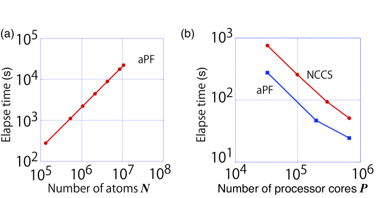
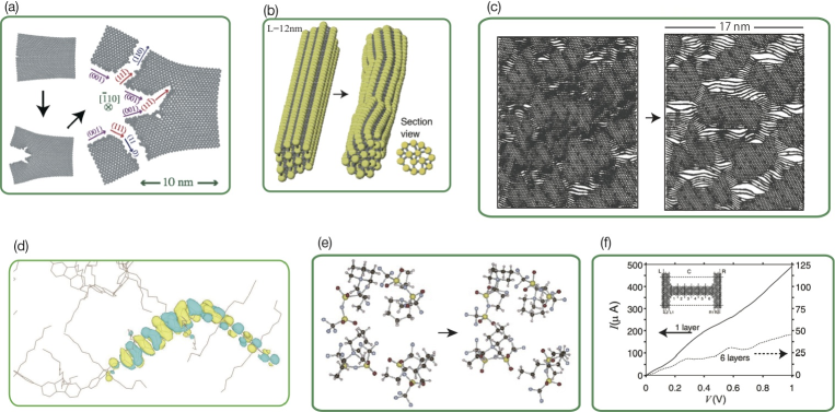
Figure 2 shows examples of nano-material studies with ELSES and related original softwares; (a) brittleness of solid silicon [3], (b) helical multishell gold nanowire [5, 9, 10] (Experimental work is Ref. [23]), (c) sp2-sp3 nano-composite carbon solid [16] in a research of nano-polycrystalline diamond [24], (d) amorphous-like conjugated polymer, [14, 19] (e) ionic liquid of N-Methyl-N-propylpiperidinium bis trifluoromethanesulfonyl imide [15], (f) quantum transport of d-band metal nanowire [6]. The studies are motivated by the view points of (i) industrial application, (ii) new material, especially new material from Japan, and (iii) standard material.
A Python-based visualization software ‘VisBAR’ [25, 16, 19] was also developed, since a post-simulation analysis of large-scale simulations requires seamless procedures of large-data-size numerical analysis and visualization. For example, Fig. 2(c) was drawn by VisBAR, when the sp2-sp3 nano-composite carbon solid [16] was analyzed for the distinction between the sp2 (graphite-like) and sp3 (diamond-like) domains. The analysis method is a quantum mechanical analysis called -type Crystalline Orbital Hamiltonian Population (COHP). The method is based on the Green’s function for electronic wavefunction and a theoretical extension of COHP [26].
3 Novel linear algebraic theory and benchmark on the K computer
The mathematical foundation of our theories is based on the ‘generalized shifted linear equation’, or the set of linear equations
| (2) |
instead of the original generalized eigen-value equation of Eq. (1). Here is a given complex number and has a physical meaning of (complex) energy. The vector is the input and the vector is the solution vector.
Recently, we have developed a set of Krylov subspace (iterative) solvers for Eq. (2); (i) generalized shifted conjugate orthogonal conjugate gradient (gsCOCG) method, [12] (ii) generalized shifted quasi-minimal residual (gsQMR) method, [13] (iii) generalized Lanczos (gLanczos) method, [12] (iv) generalized Arnoldi (gArnoldi) method, [12] (v) Arnoldi () method, [11] (vi) multiple Arnoldi method. [14] In the case of , the above theories will be reduced to the previous ones. [2, 4] The method is purely mathematical and is applicable to other scientific problems. For example, one of the above algorithms was applied to strongly-correlated electrons of La2-xSrxNiO4() [27, 7].
The multiple Arnoldi method [14] is mainly used in our simulations and Fig. 1 shows the result of benchmark. The calculated materials are amorphous-like conjugated polymer of poly-(9,9 dioctyl-fluorene) (aPF) [14, 19] and sp2-sp3 nano-composite carbon solid (NCCS). [16]. Figure 1(a) shows that the calculation has the order- scaling property [14]. Figure 1(b) shows the parallel efficiency on the K computer with one hundred million atoms. The MPI/OpenMP hybrid parallelism is used. The results are shown for a NCCS case with [19] and aPF case with (the present work). The elapse time of the electronic structure calculation for a given atomic structure is measured as the function of the number of used processor cores , from to (the total number of processor cores on the K computer). The parallel efficiency is defined as and such a benchmark is called ‘strong scaling’ in the high-performance computation society. The measured parallel efficiency for the NCCS case is , and . [19] The measured parallel efficiency for the aPF case is and .
4 ‘Novice’ and ‘expert’ modes for general users
A ‘novice’ or easy-to-use mode was developed, as well as an ‘expert’ mode, so as to give comfortable user experiences for everyone. Nowadays, quantum material simulations are popular among various researchers and many of them are not familiar to numerical algorithms and detailed procedures of the code. Such ‘novice’ users would like to use the code easily in a satisfactory computational performance with, typically, processor cores or less. ‘Expert’ users, on the other hand, would like to achieve the best computational performance for largest problems with a top-class supercomputer. Therefore we developed modes for ‘novice’ and ‘expert’ users.
The ‘novice’ and ‘expert’ modes are different in the computational costs, though they are equivalent mathematically and give the same numerical results. The ‘expert’ mode is a strict order- procedure and requires users to determine the detailed settings for the best performance, while the ‘novice’ mode contains several procedures and does not require the detailed settings. Consequently, the ‘novice’ mode is easier to use than the ‘expert’ mode but may be worse in the computational performance.
5 Use of Extensible Markup Language (XML)
In our simulations, the main input and output files are written in the format of Extensible Markup Language (XML), since the XML format is simple, flexible and widely used on the internet. For example, the minimum information for an atom is written as follows;
<atom element="C">
  <position unit="angstrom">  1.0d0  0.0d0   0.0d0  </position>
</atom>
The above description means that a carbon atom is located at the position of , where Angstrom unit (1 Angstrom = 10-10m) is used.
The method for reading XML files should be chosen properly, according to the purpose. In our simulations, the XML files are read by two methods, Document Object Model (DOM) method and Simple API for XML (SAX) method. In general, the DOM method is easier in programming and results in huge memory and time consumption for large-size data, while the SAX method is more difficult in programing and results in tiny memory and time consumption.
Two input files, configuration and structure XML files should be prepared for each simulation and they are quite different in their file size. (i) The configuration XML file describes calculation conditions, such as temperature of the system. A typical file consists of several tens of lines and the file size does not depend on the system size . The configuration file is read by the DOM method, since its file size is always tiny. (ii) The structure XML file describes the atomic structure data, as shown in the above example. The structure XML file is read by the DOM method, since the file size is proportional to the system size and can be huge. Since the atomic structure data contains three () components in the double precision (8B) value for each atom, the required data size with (=10M) atoms is estimated to be M = 240 MB. A typical size of the structure XML file with atoms is one G byte (B). In addition, the parallel file reading is used for large-scale calculations with split XML files for the structure file and gives a significant acceleration. [16] The K computer and FX10 support the parallel file IO, called ‘rank directory’ function, at the hardware level and are suitable to the parallel file reading with split XML files.
6 Sparse matrix collection and numerical ‘engine’
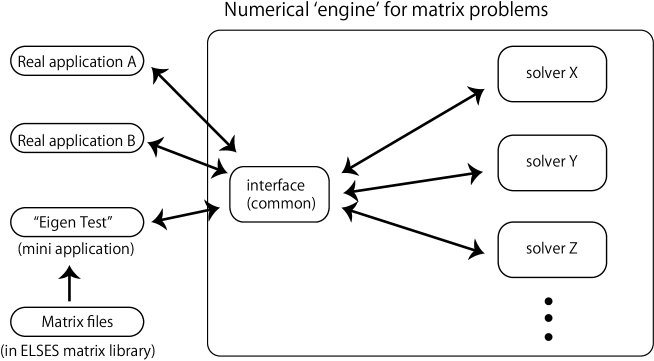
This section explains that we opened a matrix library and are developing a general numerical ‘engine’, for further collaboration between real application and numerical linear algebra.
Recently, a sparse matrix collection called ‘ELSES matrix library’ [20] was opened. The stored matrices are sparse and generated by ELSES as the matrices and in Eq. (1). The maximum matrix size is one million. Matrix data files are written in the Matrix Market format. [28] Each matrix data has its own name and appears with a document so as to clarify the physical origin of the matrix. For example, the matrix data ‘VCNT900’ presents a matrix with the size of and its physical origin is thermally vibrating carbon nanotube (VCNT). 111 The thermal vibration causes small random deviations on the atomic positions and, therefore, the calculated eigen values are not degenerated. The calculated eigen values are also included in several matrix data.
Moreover a general numerical ’engine’ for matrix (eigen-value) equations is under development with a common interface between real applications and numerical solvers. A mini application for evaluating the engine, called ‘Eigen Test’, is also under development, in which the matrix data in ELSES matrix library [20], or some files on Matrix Market [28], can be used as inputs. A code in an early version for shared memory systems is available for test users. [21] The code for distributed memory systems is under development, in which two direct solvers, ScaLAPACK [29] and EigenExa [30], are implemented for the standard and generalized eigen-value equations in the Eq. (1) with real-symmetric matrices. 222 At the present time, EigenExa does not support generalized eigen-value problems. In the engine, a generalized eigen-value problem is solved with EigenExa, since the problem is transformed into a standard eigen-value problem by the Cholesky decomposition routine in ScaLAPACK. The implementation of Krylov subspace solvers is planned. In near future, our application code ‘ELSES’ will be connected to the engine and general users can use the solvers without detailed knowledge of the solver algorithms. The engine is general and can be connected to any other real applications.
7 Internal eigen-value problem
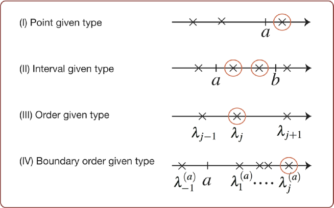
This section explains internal eigen-value problem from a general need in large-scale electronic state calculations. The present discussion is limited to real eigen-value problems. In a large-matrix problem, one should give up the calculation of all the eigen pairs, because of huge computational cost. Then one would like to obtain specific eigen pair(s) () of Eq. (1) at an internal eigen-value region (), because several internal eigen pairs are responsible for electronic and optical properties.
Internal eigen-value problems can be classified into the following four types, as illustrated in Fig. 5; (I) Point given type: For a given real value , one should find (an) eigen value(s) near the given point () and its (their) eigen vector(s). (II) Interval given type: For a given interval of (), one should find eigen values in the interval () and their eigen vectors. (III) Order given type: For a given integer of (), one should find the -th lowest eigen value () and its eigen vector. (IV) Boundary order given type: For a given integer () and a real value , one should find the -th lowest eigen value that is larger than :
| (3) |
One should find all the (degenerated) eigen vectors for the target eigen value . From the definitions, the boundary-order-given-type problem with is reduced to the order-given-type problem. In all the types of problem, if the target eigen value is degenerated, one should find all the degenerated eigen vectors.
The present paper focuses on the order-given-type problem, since the problem appears in many electronic structure calculations. In our problems, the target eigen value(s) is (are) given from the physical viewpoint. Here we call eigen value ‘level’, as usual in electronic structure calculations. Typically, the two levels, called highest-occupied (HO) and lowest-unoccupied (LU) levels, are of fundamental interest. The HO level, denoted as hereafter, is defined as the half of the total number of electrons in material () 333The present case is that of a para-spin material. and the LU level is defined as +1. For example, the difference between the two levels is called energy gap and is zero in metals and non-zero in semiconductors or insulators. Two notes are added here; (a) The levels near the HO or LU level are also of importance and are required in many electronic state calculations. (b) When is odd, the HO and LU levels are not defined in a strict physical sense. Among these cases, however, the (])-th and (+1)-th levels are still crucial for electronic properties and we call them the HO and LU levels in the present paper.
We have proposed two approaches for the order-given-type problem: One appears in Refs. [17, 18] and the other appears in Ref. [19]. See the papers for details.
Further investigations on efficient algorithms are desired for internal eigen-value problems. It is speculated that a difficulty in numerical treatment will appear among (almost) degenerated eigen pairs. An example is found in the matrix of ‘APF4686’ of ELSES matrix library [20], in which the 2345-th and 2346-th eigen values are almost degenerated (=-0.356883, = -0.356806). 444The atomic unit is used in the present eigen values
8 Physical aspect of the fundamental methodologies
The last topic is some physical (not mathematical) aspects of the fundamental methodology, in particular, ab initio based modelings in electronic structure theory. The present calculation was carried out with modeled (tight-binding-form) electronic structure theory based on ab initio calculations and sometimes a charge-self-consistent theory [31] is also used [15, 32]. The matrices and in Eqs.(1) and (2) are sparse and called the Hamiltonian and overlap matrices written the linear-combination-of-atomic-orbital (LCAO) representation, respectively. The diagonal elements of are the unity and the absolute value of an off-diagonal element is less than the unity .
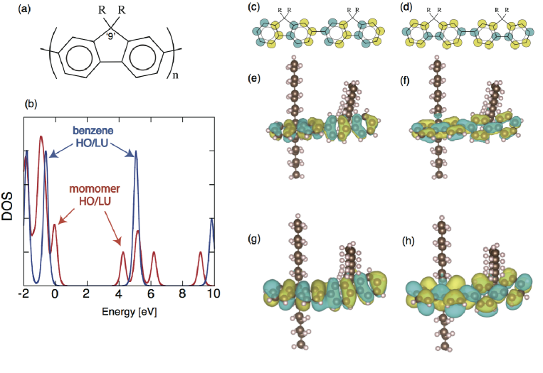
Here poly-(9,9 dioctyl-fluorene), a conjugated polymer depicted in Fig. 6(a), is picked out. The material is a basic one for opto-electronics devices. A modeled theory in Ref [33] is used and it is called the atomic-superposition and electron-delocalization tight-binding (ASED-TB) theory. The monomer unit in Fig. 6(a) consists of two benzene rings and alkyl side chains of C8H17. The letter ‘9’ indicates the atom site called ‘9-position’, located at the ‘root’ part of the side chain or the top site of the five-membered ring. The side chains are extended transversely, since the ‘9-position’ in Fig. 6(a) has an -like electronic configuration and the neighboring four atoms form tetrahedral bonds.
The monomer and dimer were calculated with the exact solution of Eq. (1). The density of states (DOS) function, a eigen-value histogram, is shown in Fig. 6(b) for the monomer and a benzene molecule (C6H6). The HO and LU electronic wavefunctions of the dimer are drawn schematically in Fig. 6(c)(d), respectively and the calculated HO and LU wavefunctions with the optimized structure are shown in Fig. 6(e)(f), respectively. The two monomer units of the dimer are connected with twisting, as shown in Fig. 6(e) or (f), mainly because of the repulsion between the hydrogen atoms on the benzene rings of the neighboring monomers. The half of Fig. 6(c) or (d) corresponds to the schematic figure of the HO or LU state of the monomer, [34] respectively. The wavefunctions are contributed only by the -type wavefunctions on the benzene rings. The HO wavefunction of the dimer and the monomer has two nodes on a benzene ring, and the LU wavefunction of the dimer and the monomer has four nodes on a benzene ring. These node structures are the same with those of a benzene, [34] because the HO and LU levels of the monomer stem from those of benzene, which is seen in the DOS functions of Fig. 6(b). The monomer and dimer are calculated also by the ab initio calculation (Gaussian 09(TM)) with the B3LYP functional and the 6-31G(d,p) basis set and the above features of wavefunctions are satisfied in the calculated HO and LU wavefunctions shown in Figs. 6(g)(h). The atomic structures and the DOS functions were also calculated and satisfy the above features. Moreover, detailed data by the present method are added here with those by the ab initio calculation in the parentheses; [14] The balance band width and the band gap are eV (18.3 eV) and eV (4.91 eV) in the monomer and eV (18.8 eV) and eV (4.10 eV) in the dimer. The twisting angle of the dimer is (40.6 ∘).
Several notes are posted on the transferability (general applicability) of model theories; (i) The present theory is formulated without any data of fluorene cases but is formulated with related small molecules such as benzene. The above agreement with the ab initio calculations in the fluorene cases shows that the theory is applicable to, at least, materials that have similar binding mechanisms. (ii) Quite recently, a modeled van der Waals (vdW) interaction [35] is implemented in the code for wider applicability to materials. Details will be discussed elsewhere. (iii) Automated determination methods for obtaining an optimal model among various materials is desired and is now developing with ELSES [32, 36].
9 Summary and future outlook
The present paper reports our methods and results of large-scale electronic structure calculations based on our novel linear algebraic algorithms. A high parallel efficiency was shown in one-hundred-million-atom systems with up to all the built-in cores of the K computer. The related methodologies on physics, mathematics and information technology are also discussed.
The present study is a interdisciplinary one between physics, numerical linear algebra and high-performance computation techniques, and such a interdisciplinary study is sometimes called ’Application-Algorithm-Architecture co-design’. The co-design will play a crucial role in exa-scale scientific computations.
Acknowledgments.
This research is partially supported by Grant-in-Aid for Scientific Research (KAKENHI Nos. 23540370 and 25104718) from the Ministry of Education, Culture, Sports, Science and Technology (MEXT) of Japan. The K computer was used in the research proposals of hp120170, hp120280 and hp130052. Several calculations were carried out by the supercomputer at the Information Technology Center, University of Tokyo, in the research proposal of jh130011-NA07. Supercomputers were also used at the Institute for Solid State Physics, University of Tokyo, and at the Research Center for Computational Science, Okazaki.References
- [1] ELSES(=Extra Large-Scale Electronic Structure calculation): http://www.elses.jp/
- [2] R. Takayama, T. Hoshi and T. Fujiwara, Krylov subspace method for molecular dynamics simulation based on large-scale electronic structure theory , J. Phys. Soc. Jpn.73 (2004) 1519. [cond-mat/0401498]
- [3] T. Hoshi, Y. Iguchi, and T. Fujiwara, Nanoscale structures formed in silicon cleavage studied with large-scale electronic structure calculations: Surface reconstruction, steps, and bending, Phys. Rev. B 72 (2005) 075323. [cond-mat/0409142]
- [4] R. Takayama, T. Hoshi, T. Sogabe, S.-L. Zhang, and T. Fujiwara, Linear algebraic calculation of the Green’s function for large-scale electronic structure theory , Phys. Rev. B 73 (2006) 165108. [cond-mat/0503394]
- [5] Y. Iguchi, T. Hoshi, T. Fujiwara, Two-stage formation model and helicity of gold nanowires Phys. Rev. Lett. 99 (2007) 125507. [cond-mat/0611738]
- [6] H. Shinaoka, T. Hoshi and T. Fujiwara, Ill-Contact Effects of d-Orbital Channels in Nanometer-Scale Conductor, J. Phys. Soc. Jpn. 77 (2008) 114712. [cond-mat/arXiv:0809.3078]
- [7] S. Yamamoto, T. Sogabe, T. Hoshi, S.-L. Zhang and T. Fujiwara, Shifted Conjugate-Orthogonal-Conjugate-Gradient Method and Its Application to Double Orbital Extended Hubbard Model , J. Phys. Soc. Jpn. 77 (2008) 114713. [cond-mat/arXiv:0802.2790]
- [8] T. Sogabe, T. Hoshi, S.-L. Zhang, and T. Fujiwara, On a weighted quasi-residual minimization strategy of the QMR method for solving complex symmetric shifted linear systems , Electron. Trans. Numer. Anal. 31 (2008) 126.
- [9] T. Hoshi, T. Fujiwara, Domain boundary formation in helical multishell gold nanowire , J. Phys.: Condens. Matter 21 (2009) 272201. [cond-mat/arXiv:0808.1353]
- [10] T. Hoshi,Y. Iguchi and T. Fujiwara, Ultrathin gold nanowires, Handbook of Nanophysics : Nanotubes and Nanowires , Ed. Klaus D. Sattler, CRC Press, pp.36.1-18, (2010).
- [11] T. Yamashita, T. Miyata, T. Sogabe, T. Fujiwara, S.-L. Zhang, An Arnoldi (M, W, G) Method for Generalized Eigenvalue Problems, Trans of JSIAM 21 (2011) 241 (Japanese).
- [12] H. Teng, T. Fujiwara, T. Hoshi, T. Sogabe, S.-L. Zhang, and S. Yamamoto, Efficient and accurate linear algebraic methods for large-scale electronic structure calculations with nonorthogonal atomic orbitals, Phys. Rev. B 83 (2011) 165103. [cond-mat/arXiv:1101.4768]
- [13] T. Sogabe, T. Hoshi, S.-L. Zhang, and T. Fujiwara, Solution of generalized shifted linear systems with complex symmetric matrices, J. Comp. Phys. 231 (2012) 5669.
- [14] T. Hoshi, S. Yamamoto, T. Fujiwara, T. Sogabe, S.-L. Zhang, An order- electronic structure theory with generalized eigenvalue equations and its application to a ten-million-atom system, J. Phys.: Condens. Matter 21 (2012) 165502. [cond-mat/arXiv:1202.0098]
- [15] S. Nishino, T. Fujiwara, H. Yamasaki, S. Yamamoto, T. Hoshi, Electronic structure calculations and quantum molecular dynamics simulations of the ionic liquid PP13-TFSI, Solid State Ionics 225 (2012) 22.
- [16] T. Hoshi, Y. Akiyama, T. Tanaka and T. Ohno, Ten-million-atom electronic structure calculations on the K computer with a massively parallel order-N theory, J. Phys. Soc. Jpn. 82 (2013) 023710. [cond-mat/arXiv:1210.1531]
- [17] D. Lee, T. Miyata, T. Sogabe, T. Hoshi, S.-L. Zhang, An interior eigenvalue problem from electronic structure calculations, Japan J. Indust. Appl. Math. 30 (2013) 625-633.
- [18] D. Lee, T. Miyata, T. Hoshi, and S.-L. Zhang, An interior eigenvalue problem and its numerical solution, in The 9th East Asia SIAM Conference The 2nd Conference on Industrial and Applied Mathematics (EASIAM-CIAM 2013) , Institut Teknologi Bandung, Bandung, West Java, Indonesia, 18-20., June. 2013
- [19] T. Hoshi, K. Yamazaki, Y. Akiyama, Novel linear algebraic theory and one-hundred-million-atom electronic structure calculation on the K computer, in press, [http://arxiv.org/abs/1307.3218].
-
[20]
ELSES matrix library:
http://www.elses.jp/matrix/ -
[21]
Eigen Test:
http://www.damp.tottori-u.ac.jp/~hoshi/eigen_test/ - [22] W. Kohn, Density functional and density matrix method scaling linearly with the number of atoms . Phys. Rev. Lett. 76 (1996) 3168.
- [23] Y. Kondo and K. Takayanagi, Synthesis and characterization of helical multi-shell gold nanowires , Science 289 (2000) 606.
- [24] T. Irifune, A. Kurio, A. Sakamoto, T. Inoue, and H. Sumiya, Materials: Ultrahard polycrystalline diamond from graphite , Nature 421 (2003) 599.
-
[25]
VisBAR(=Visualization tool with Ball, Arrow and Rods):
http://www.damp.tottori-u.ac.jp/~hoshi/visbar/ -
[26]
R. Dronskowski , P. E. Blöchl,
Crystal orbital Hamilton populations (COHP):
energy-resolved visualization of chemical bonding
in solids based on density-functional calculations
,
J. Phys. Chem. 33, 97 (1993);
http://www.cohp.de/ - [27] S. Yamamoto, T. Fujiwara, and Y. Hatsugai, Electronic structure of charge and spin stripe order in La2-xSrNiO4() , Phys. Rev. B 76 (2007)165114.
-
[28]
Matrix Market:
http://math.nist.gov/MatrixMarket/ -
[29]
ScaLAPACK:
http://www.netlib.org/scalapack/ -
[30]
EigenExa:
http://www.aics.riken.jp/labs/lpnctrt/EigenExa_e.html - [31] M. Elstner, D. Porezag, G. Jungnickel, J. Elsner, M. Haugk, T. Frauenheim, S. Suhai, G. Seifert, Self-consistent-charge density-functional tight-binding method for simulations of complex materials properties, Phys Rev B 58 (1998) 7260.
- [32] S. Nishino and T. Fujiwara, Parametrization scheme with accuracy and transferability for tight-binding electronic structure calculations with extended Hückel approximation and molecular dynamics simulations, J. Mol. Model. 19 (2013) 2363.
- [33] G. Calzaferri and R. Rytz, The Band Structure of Diamond, J. Phys. Chem. 100, 11122 (1996).
- [34] The HO and LU wavefunctions of benzene are found in elementary textbooks, such as, P. W. Atkins, R. S. Friedman, Molecular Quantum Mechanics, fifth ed., Oxford University Press, Oxford (2010).
- [35] F. Ortmann and F. Bechstedt and W. G. Schmidt, Semiempirical van der Waals correction to the density functional description of solids and molecular structures, Phys Rev B 73 (2006) 205101.
- [36] Y. Ohtani, T. Fujiwara, S. Nishino, T. Suzuki, S. Yamamoto and Y. Zempo, Automatic determination of tight-binding parameters in bulk systems, MRS Proceedings 1523 (2013) mrsf12-1523-qq06-08