The two-step photoexcitation mechanism in a-Se
Abstract
The first-principal simulations are applied to study a photo-induced metastability in amorphous selenium (a-Se) and the contribution of the valence-alteration pair (VAP) defects in this process. The VAP defect is confirmed to be the equilibrium defect; it minimizes the destabilizing interaction between adjacent Se chains induced by dis-orientation of the lone-pair (LP) electrons, and thus relieves a tension in a system. The excitation of LP electrons is proposed to be described by two coexisting processes, namely, single and double electron excitations. Both processes have been found to form defect states in the band gap and to cause the experimentally observed photo-darkening and photo-volume expansion, however, only double electron excitation is capable to trigger bond rearrangement and structural transformation. Lattice relaxation, which follows bond rearrangement occurs with characteristic energy of -0.90.3 eV and promotes formation of energetically favorable VAP defects or crystalline inclusions thus ultimately stimulating the photo-induced crystallization. In addition, photo-induced crystallization has been directly simulated in a system with an increased crystalline order.
I Introduction
The progressively expanding area of applications of chalcogenide glasses (from medical imaging detectors to phase-change memories) supports an irrefutable interest in their properties, one of which is photoinduced transformation - a very unique phenomenon that is a special feature of chalcogenide glasses including amorphous Se. The transformation is known to be triggered by optical or x-ray irradiation and is associated with a creation of defects 1 ; 2 ; 3 . The most studied defect in amorphous Se is a valence-alteration pair (VAP) 1 ; 2 ; 3 ; 4 ; 5 which belongs to equilibrium type of defects 4 meaning that VAP exists in well relaxed structure prior to photoexcitation. However, photoexcitation is assumed to enhance a concentration of the VAP defects by initiating the bond breaking reaction: 2CC+C, where C is a selenium atom in its normal two-fold configuration, C is a positively charged three-fold configuration, and C is a negatively charged one-fold coordinated Se atom 1 . The direct evidence of the valence alteration in a-Se is experimentally detected unpaired electrons which appear under light illumination 2 . It is believed that the VAP defects are responsible for many of the photoinduced effects including photodarkening (PD) 6 ; 7 ; 8 , photoinduced crystallization 7 and volume expansion 13 ; 14 ; 15 as they induce the sub-band gap defect states 9 ; 10 ; 11 ; 19 . Although a link between these effects is not confirmed with direct experiments, they all have similar kinetics and are shown to be thermally activated processes with similar activation energies around 0.9 eV 6 ; 7 - the value which was suggested for the VAP defect relaxation 12 .
In order to get a better insight into the nature of the photoinduced effects and contribution of the VAP defects in it, we model the entire process of photoexcitation with help of the first-principles methods. First, we have classified all possible VAP defects in a-Se network, their energetics and positions in the band gap. Then, we have simulated a photoexcitation from an ”ideal” system (consisting of strictly two-fold coordinated Se atoms) and a system containing the VAP defect. We show that in both systems the excitation of two electrons from the lone pair (LP) state may trigger a formation of a dynamic bond with the characteristics energy -0.90.3 eV through the photo-induced relaxation of the immediate neighborhood. In post-excitation regime, this dynamic bond is broken which then induces the bond rearrangement followed by a creation either of the VAP defect or the crystalline inclusion. In contrast, removal of just one electron from the LP state does not generate any significant lattice relaxation and, therefore, does not lead to a permanent structural transformation. The simulated photo-induced transformations show good correlation with the PD kinetics measured under the red light illumination. The comparison with the experimental results suggests that the slow component in the kinetics of the photodarkening relaxation can be linked to the process which involves the bond rearrangements (i.e. when two electrons are photoexcited from the LP state) with the experimentally found activation energy EB=0.80.1 eV. In contrast, the fast component in the photodarkening relaxation corresponds to a process which does not involve any significant lattice relaxation that is observed in simulations of a single electron excitation.
II Theoretical methods
For our study, we created the model compounds of amorphous Se consisting of 25 atoms and 50 atoms. For the atomistic simulations, the WIEN2k package 16 with implementation of the Perdew-Burke-Ernzerhof parametrization of the generalized gradient approximation 17 has been used. The optimization procedure was carried based on minimization of forces for which the product of atomic sphere radius (1.8 Bohr centered at the nucleus of the individual atoms) and plane-wave cutoff in -space was set to 7, while the Brillouin zone of a supercell was covered by the 444 Monkhorst-Pack mesh. The energy separating core and valence electrons was set to -6.0 Ryd. The force tolerance 0.5 mRyd/Bohr in combination with tight convergence limits (energy convergence 0.0001 Ryd, force convergence 0.1 mRyd/Bohr and charge convergence 0.001 e) have been applied.
To study the fundamental properties of a-Se including the formation of the VAP defects and photo-induced structural transformations, the well amorphized a-Se placed in cubic supercell (=90∘, =90∘, =90∘) with periodic boundary conditions was used (the size of the cubic supercell consisting of 25 atoms was 8.7Å8.7Å9.9Å). In order to insure that the inter-cell defect interaction does not effect the energetics of the VAP defects, the results have been verified with a bigger supercell consisting of 50 atoms. The size of the Monkhorst-Pack mesh was adjusted to the supercell size, i.e. the mesh was appropriately reduced as the supercell was enlarged. In the created model compounds, the bond length between two-fold sites was found to vary in a range of 2.30-2.47 Å that agrees well with an average bond length in a-Se of 2.37 Å 12 ; 13 . The bond angles along the chains in the well amorphized system have shown to vary from 98∘ to 107∘ against 102∘ in trigonal Se (t-Se). For the simulations of the photo-induced crystallization, the system of the increased crystalline order has been created. To achieve crystallization, the model system has been assigned to recognize the symmetry of trigonal Se through application of the hexagonal lattice parameters to supercell (=90∘, =90∘, =120∘).
III The VAP defects and their classification
We start our analysis from the ”ideal” amorphous system containing only two-fold coordinated Se atoms, each having two electrons on the -bonding orbital, two empty quantum states on the -anti-bonding orbital and two electrons on the nonbonding LP orbital. The properties of such ”ideal” network are governed by the lone pairs: by pushing the shared orbitals apart, they define the bond angle and torsion angle. The crystalline systems, i.e. trigonal and -monoclinic Se, are built in a way to minimize interatomic interactions of the LP electrons. In amorphous network, LPs are disoriented that causes tension between chains and as a result, the total energy is larger by =0.08 eV per atom than that in t-Se due to the destabilizing interactions between chains. The charge exchange between Se atoms in amorphous network (up to 0.5 per atom) is an attempt to reduce the chain tension. Naturally, the crystalline-like inclusions suppress the tension. We estimated that formation of a Se7 ring results in energy lowering by =-0.02 eV per atom.
With respect to the electronic properties, disorientation of LPs causes formation of the band tails. The edge of the valence band (EV) generated by the lone pairs is found to be smeared by the broad tails as defined by EV=EV+0.45 eV. Because bottom of the conduction band (EC) is formed by -antibonding orbitals, the effect of LP disorientation is less pronounced there 18 giving a rise to the band tails of a size of EC=EC-0.16 eV. This simulated asymmetry in the band tails has also been observed experimentally 9 ; 10 . It has to be mentioned that an inclusion of a Se7 ring locally improves the LPs orientation resulting in total band tails shrinkage by 0.3 eV with most pronounced effect near the valence band.
In addition to crystalline-like inclusions, another way to resolve the destabilizing interactions between two chains is chain discontinuation CC+C. When chain breaks, one C end remains as the separated site, while another connects to two-fold C site of another chain thus becoming three-fold C (see defect structure in Fig. 1 (a)). This process is followed by the charge exchange reaction C+CC+C (see charge distribution in Fig. 1 a) and formation of two chains VAP defect 2 ; 3 . We have found that the total energy lowering with this defect formation is =-0.05 eV per atom (since this value is calculated per all atoms in a supercell, it is underestimated for atoms involved in the VAP formation). Therefore, we numerically confirmed that the two chains VAP defect is very efficient in relieving tension between chains despite a strong dipole formed between the C and C sites. With respect to the defect structure, the C and C sites are separated by a distance 3.45 Å, while the bond length around C is slightly elongated to 2.4-2.6 Å due to the bond iconicity.
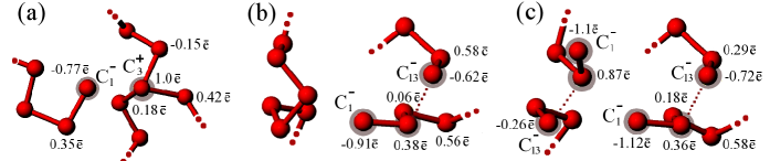
When broken C end connects to the same chain, another type of the VAP defect emerges (see Fig. 1 b) 5 which is named in literature as ”intimate” VAP defect (IVAP) 5 . We have found that the IVAP defect is stable only in the intimate configuration. Mechanism of formation of the IVAP defect is the same as for VAP (Fig. 1 a), one broken end remains detached while second attempts to convert into three-fold site denoted in Fig. 1 b as C. Because the induced charge redistribution is restricted to a single chain, the originated strong dipole keeps apart the C and C sites at distance =2.82 Å (see a dashed line in Fig. 1 b). Moreover, a strong dipole moment masks the stress relieving effect and as a result, no decrease in energy is detected with this defect formation. However, when two IVAP defects appear in a pair (see Fig. 1 c showing two IVAP defects separated by a distance 3.8 Å), the interaction between defects induces the partial compensation of their dipoles. It allows the bond shortening between C and C sites to =2.78 Å and uncovers the stress relieving effect resulting in the energy lowering by =-0.04 eV per atom. The IVAP pair is found here for the first time. Since the total energy decreases with pair formation, this pair configuration should dominate over single IVAP.
Overall, the ”ideal” system has found to be the highest in energy. Therefore, the VAP defects or crystalline inclusions such as the Se8, Se7 and Se6 rings 20 are thermodynamic defects 4 which formation reduce the stress originated from LPs dis-orientation. As a result, in a-Se grown samples, there will always be interplay between concentration of the rings and the VAP defects. The preference would be given to formation of the VAP defects (Fig. 1 a) as they are most efficient in relieving tension between chains reflected by the greatest energy reduction =-0.05 eV per atom. This explains the low concentration of the rings observed experimentally (fraction of atomic rings is 5-10 21 ; 22 ). In regions under enhanced stress such as interfaces, the higher concentration of the tension relieving centers is expected.
The VAP defects have direct impact on the electronic properties of a-Se. According to our calculations, the defect states generated by C appear below the conduction band at EC-0.33 eV for the two chains VAP; at EC-0.43 eV for the single IVAP; and at EC-0.61 eV for the IVAP pair. The energetic positions of the defect states induced by C agrees well with the experimental observation showing two peaks in the density of states at 0.30 eV and 0.450.50 eV below EC 10 that is also consistent with the positions of the charged centers in Ref.11 . The C states are located above the valence band at EV+0.34 eV for the VAP and the single IVAP defects, and at EV+0.23 eV for the IVAP pair. Therefore, the C states appear inside the valence band tails defined by EV=+0.45 eV. Depending on the concentration of the VAP, single IVAP and IVAP pairs, they may influence the density of state distribution causing characteristic features at about 0.23 eV and 0.34 eV above the valence band as observed in some experiments 9 .
Therefore, our finding confirms that the VAP defects are the thermodynamic or the ”equilibrium” type as suggested in literature 4 , i. e. they should be present at high concentration in the well-relaxed structures even prior to light excitation. Since the formation of the VAP defects and the crystalline inclusions in a form of the Se7 ring are energetically favorable, their concentration should grow under light illumination. Hence, our next step is a simulation of the photoinduced changes in amorphous Se network.
IV Photo-induced lattice relaxation
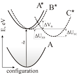
The photoexcitation process can be described with potential diagram presented in Fig. 2. The excitation of electrons brings the system from a ground state A to an excited state A∗. We assume that an electron excited into the conduction band leaves behind the hole in the valence band tails. The state in the valence band tails missing one or two electrons induces the lattice relaxation of the immediate neighborhood needed for its stabilization. As a result, the excited A∗ state converts either into B∗ or C∗ state. The B∗ state accounts for the insignificant lattice relaxation involving no bond rearrangements as denoted by small energy lowering UEB. In contrast, the C∗ state occurs with bond rearrangements reflected in large UEC. The A∗C∗ transfer requires overcoming the potential barrier VB. When missing electrons return, only the B∗ state would be able to relax into the original ground state A.
The sub-bandgap excitation occurs primarily from the top of the valence band formed by the LP electrons: for the ”ideal” system an excitation involves the partially charged C sites, while for the VAP defects the C sites are those who participate. Upon excitation, the LP occupancy is reduced by one electron (LPLP1) and the LP1 state with unpaired electron is shifted deeper into the bandgap by 0.2 eV due to an alteration in the exchange interaction upon removal of an electron. The LP1 states induce the PD effect and are detected experimentally due to a presence of the unpaired electrons 2 . The electron density of the LP1 state is delocalized over several sites: our calculations show that it involves up to 5 sites for the two chains VAP defect. The relaxation of the immediate neighborhood around the LP1 state required for its stabilization is found to be accompanied by the bond shortening/elongation occurring with characteristic energy U-0.1 eV that corresponds to the B∗ state in Fig. 2. The bond shortening is observed for the IVAP defects (see Fig. 1 b,c). The bond shortens by 0.1 Å that agrees with previous findings 13 . In contrast, the double chain VAP defect shows a significant increase in a distance between the C and C sites by 0.25 Å. Because the concentration of the double chain VAP defects should dominate over other defects, an increase in a separation between C and C sites would govern volume expansion observed experimentally 14 . Since the bond elongation occurs with the characteristic energy UEB, it is not an immediate process. Therefore, the volume expansion caused by LP1 states at the double chain VAP defect is expected to be delayed from the PD onset that agrees with the experimental observations 14 . When the missing electron returns (LPLP2), all systems have been found to come back to the original state A.
It should be noted that for the formation of the photo-induced robust dynamic bond known as the C3-C3 defect 2 ; 3 , an excitation of two electrons in a vicinity of a single site is required that is also simulated here as LPLP0 process (LP0 appears above the LP1 position in the band gap). Because excitation of two electrons is unlikely to occur simultaneously, two possible scenarios are considered. (i) LPLP0: inequality in the charge distribution generated by LP1 promotes excitation of the second electron from the vicinity of the same site. (ii) LP1+LP1LP0+LP2: two interacting LP1 states undergo charge exchange. The latter process becomes feasible when the energy lowering due to the lattice relaxation needed for stabilization of the LP0 state is greater than 2UEB accounted for two interacting LP1 states.
The double electron excitation has been simulated by successive removal of two electrons from the system. For the ”ideal” two-fold coordinated system and the IVAP pair defect (Fig. 1 c), the significant lattice relaxation with the characteristics energy UEC=-0.90.3 eV is followed by the bond rearrangements (the C∗ state in Fig. 2). In the ”ideal” two-fold coordinated system, the C3-C3 dynamic bond occurs through crosslinking between two chains 2 ; 3 . The defect state induced by the C3-C3 dynamic bond appears close to the midgap. Following lattice relaxation, two unequally populated LP1 sites formed upon excitation are converted into the LP0 and LP2 states, i.e. the charge transfer reaction LP1 + LP1LP0 + LP2 is initiated since system meets the requirement UU. For the IVAP pair defect, the double excitation has been found to induce bond rearrangements followed by formation of the single C3 defect with three equivalent bonds 2.4-2.5 Å (the defect state appears closer to the conduction band). To reach the final configuration, the lattice relaxation requires overcoming the potential barrier V0.8 eV. It correlates well with the potential diagram presented in Fig. 2 for A∗C∗ transition. However, some configurations have shown to be resistant to the double electron excitation because destabilization induced by the hole localized in the valence band tails is not enough to overcome the potential barrier VB. Thus, for the two chains VAP and the single IVAP defects, the B∗ state with characteristic relaxation energy U -0.1 eV occurs predominantly.
When two missing electrons are returned into the system, the C∗ state becomes unstable and its stabilization requires breaking the dynamic or other bonds that depends on whether the dynamic bond is strongly stabilized at the excited state or not. The process of bond breaking and switching in the post-excitation regime is found to occur with the characteristic energy -0.90.3 eV which is similar to UEC. In this case, the final configuration is different from the original ground state A (Fig. 2). The ”ideal” system has been converted into one containing the S7 ring; decrease in the total energy as compared with the initial configuration is found to be 0.49 eV. The IVAP pair (Fig. 1 c) is converted into the double chain VAP defect (Fig. 1 a) accompanied by the lowering in energy by 0.28 eV. Therefore, we conclude that following the sub-bandgap illumination which involves excitation of the LP electrons, the system goes into the most stable state characterized by the increased concentration of the S7 ring and/or the VAP defects.
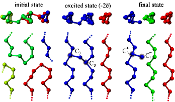
Since the double electron excitation is sufficient to induce the bond rearrangements, we attempt to generate the photocrystallization in the increased crystalline order system as shown in Fig. 3. The electron excitation is found to induce the formation of the standard C3-C3 defect followed by chain straightening (see the excited state in Fig. 3). In post-excitation regime, the complete conversion to t-Se is achieved. Because of the increased crystalline order of the initial system, the characteristics energies describing the lattice relaxation is found to be U-0.50.3 eV that is lower than that for the well amorphized systems. Therefore, we suggest that experimentally observed crystallization of the a-Se samples under sub-bandgap illumination 7 ; 23 should be linked to the double electron excitation process.
V The structural transformations in PD kinetics
In order to verify that both single and double electron excitations are plausible processes involved in photoexcitation, the kinetics of PD in a temperature range between room temperature and 40 ∘C have been studied experimentally (the upper temperature limit is dictated by a-Se glass transition temperature). The PD experiments were carried out on 15m thick stabilized a-Se layer (with 0.5 of As) using standard two red laser beams setup (655 nm), where a powerful pump beam (150 mW/cm2) was used to produce photodarkening while less powerful probing beam (0.29 mW/cm2) monitored changes in transmission of light T. The detailed descriptions of the experimental apparatus can be found in the previous work 6 .
The kinetics of PD were studied by periodically exposing the a-Se sample to the pumping beam for 200 s separated by 200 s of rest. During those cycles, the probing beam transmission, T, is continuously monitored and the relative changes compared to the original transmission of light, T/T0, were then calculated. The restoration of the transmission during the rest period at room temperature and selected elevated temperatures is shown in Fig. 4 and can be modeled by the double-exponential decay yielding two characteristic time constants: and . At room temperature, the characteristic relaxation times and derived from fitting of the resting cycles are 85 s and 2.5 s, respectively, after averaging over several cycles. Remarkably, decreases with increase in temperature showing the Arrhenius dependence:
| (1) |
where is the Boltzmann constant, is the temperature and is the attempt-to-escape frequency. It yields the activation energy EB=0.80.1 eV (=1011s-1). In contrast, remains temperature independent for all applied temperatures.
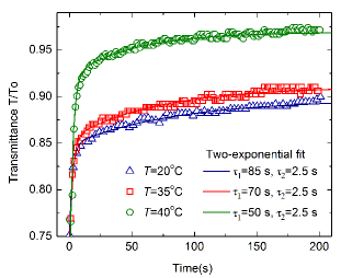
This clearly demonstrates that relaxation of PD involves two distinct processes: one that has the lattice relaxation in its origin and requires activation over a potential barrier with characteristic time , and another process which does not involve the lattice relaxation and occurs much faster with . The remarkable similarities between the magnitude of the activation energy EB=0.80.1 eV found in PD experiment and UEC=-0.90.3 eV required for the bond rearrangements, makes us to believe that this slow component in PD describes the process of structural relaxation with the bond rearrangements. Therefore, a feasibility of the process of double electron excitation accompanied by formation of the LP0 states is confirmed by slow component of the PD relaxation. Taking into the account two plausible scenarios for the LP0 sites formation (LPLP0 or LP1+LP1LP0 + LP2), we suggest that concentration of the LP0 states should depend non-linearly on the rate of excitation.
In contrast, the temperature independence of the fast component (=2.5 s) is the direct evidence of the relaxation process that does not involve bond rearrangements. It is consistent with very weak lattice relaxation U-0.1 eV involved in stabilization of the LP1 states generated by the single electron excitation. The experimental detection of the unpaired electrons 2 which can be associated only with the LP1 states is further evidence of the single-electron excitation.
VI Conclusions
The first-principal methods are applied to simulate the photoinduced structural transformations in a-Se network that has allowed for the compilation of the complete picture of the photo-induced changes. Our calculations suggest two distinct mechanisms of the photo-excitation, i.e. the single electron and double electron excitation, which are followed by different lattice relaxation processes. The excitation of a single electron from LP2 leaves behind an unpaired electron and shifts the non-bonding LP1 state towards the midgap thus inducing the photodarkening effect. This process manifests itself in the fast component of the relaxation of the photodarkening which is characterized by short and temperature independent characteristic time constant =2.5 s. The fact that is temperature independent suggests that no bond rearrangement is involved in the lattice relaxation. Since the hole localized at the LP1 site does not trigger the bond rearrangements, the single electron excitation can not be accounted for the photo-induced crystallization. However, it is responsible for the photo-induced volume expansion 14 as the LP1 states appearing at the double chain VAP defect increase a separation between the C and C sites.
In order to trigger the structural transformation in the a-Se network,
excitation of two electrons from the vicinity of the same LP is required.
The characteristics energy of the lattice relaxation following the
formation of the C3-C3 defect is found to be UEC=-0.90.3 eV.
This process is reflected in the slower component of the PD relaxation described
by the temperature dependent time constant =85 s yielding the activation energy of
EB=0.80.1 eV. The similarity between the characteristics energy describing
the lattice transformation UEC and the activation energy EB in the PD kinetics
suggests their same origin.
In addition, the application of the double electron excitation to the system of
the increased crystalline order has found to induce photocrystallization.
VII Acknowledgement
The computational facilities have been acquired through membership in Shared Hierarchical Academic Research Computing Network (SHARCNET:www.sharcnet.ca) and Compute/Calcul Canada. Authors are also thankful to Dr. Safa Kasap for stimulating discussions and to Dr. O. Rubel for sharing his computational clusters. Financial support of Ontario Ministry of Research and Innovation through a Research Excellence Program Ontario is highly acknowledged.
References
- (1) M. Kastner, D. Adler, and H. Fritzsche, Phys. Rev. Lett. 37, 1504 (1976).
- (2) A.V. Kolobov, M. Kondo, H. Oyanagi, A. Matsuda, K. Tanaka Phys. Rev. B 58, 12004 (1998).
- (3) A. Kolobov, H. Oyanagi, K. Tanaka, K. Tanaka, Phys. Rev. B, 55,726, (1997).
- (4) J. Rowlands, S. Kasap, Physics Today, 50, 24 (1997).
- (5) S. R. Elliott, Physics of Amorphous Materials, (Longman, Essex, 1990).
- (6) A. Reznik, B. J. M. Lui, J. A. Rowlands, S. D. Baranovskii, O. Rubel, V. Lyubin, M. Klebanov, S. O. Kasap, Y. Ohkawa, T. Matsubara, K. Miyakawa, M. Kubota, K. Tanioka, and T. Kawai, J. Appl. Phys. 100, 113506 (2006).
- (7) R. E. Tallman, A. Reznik, B. A. Weinstein, S.D. Baranovskii and J.A. Rowlands, Appl. Phys. Lett. 93, 212103 (2008).
- (8) A. Reznik, S. D. Baranovskii, M. Klebanov, V. Lyubin, O. Rubel, and J.A. Rowlands J. Mater. Sci: Mater. Electron. 20, S111 (2009)
- (9) J. Hegedus, K. Kohary, D. G. Pettifor, K. Shimakawa, S. Kugler, Phys. Rev. Lett. 95, 206803 (2005).
- (10) K. Tanaka, Phys. Rev. B 57, 5163 (1998).
- (11) R. Lukacs, S. D. Baranovskii, P. Thomas, F. Gebhard, J. Appl. Phys. 103, 093541 (2008).
- (12) K. Koughia, S. O. Kasap, J. Non-Crystal. Solids 352, 1539 (2006);
- (13) K. Koughia, Z. Shakoor, S. O. Kasap and J.M. Marshall, J. Appl. Phys. 97, 033706 (2005).
- (14) M.L. Benkhedir, M.S. Aida, G.J. Adriaenssens, J. Phys. Condens. Matter 20, 215202 (2008).
- (15) Charge Transport in disordered solids, S.D. Baranovski, (ed), John Wiley & Sons, Ltd, Chichester, (2006). p. 156.
- (16) K. Tanaka, J. Non.-Crystalline Solids 59-60, 925 (1983).
- (17) Blaha P, Schwarz K, Madsen G K H, Kvasnicka D and Luitz J Wien2k: An Augmented Plane Wave + Local Orbitals Program for Calculating Crystal Properties: Karlheinz Schwarz, (Techn. Universität Wien, Austria, 2001)
- (18) J.P. Perdew, K. Burke, and M. Ernzernof, Phys. Rev. Lett. 77, 3865 (1996).
- (19) C. K. Wong, G. Lucovsky, J. Bernholg, J. Non-Crystalline Solids 97&98, 1171-1174 (1987)
- (20) X. Zhang, D.A. Drabold, J. Non-Crystalline Solids 241, 195 (1998).
- (21) G. Lucovsky, in: E. Gerlach, P. Grosse (Eds.). The Physics of Selenium and Tellerium, Springer, New York, 1979, p. 178
- (22) S. N. Yannopoulos, K.S. Andikopoulos, J. Chem. Phys. 121, 4747 (2004).
- (23) A. Reznik, B. J. M. Lui, V. Lyubin, M. Klebanov, Y. Ohkawa, T. Matsubara, K. Miyakawa, M. Kubota, K. Tanioka, and T. Kawai, J. A. Rowlands, Journal of Non-Crystalline Solids, 352, 1595 (2006).