Coplanar waveguide based ferromagnetic resonance in ultrathin film magnetic nanostructures: impact of conducting layers
Abstract
We report broadband ferromagnetic resonance (FMR) measurements based on a coplanar waveguide (CPW) of ultrathin magnetic film structures that comprise in-plane/out-of-plane decoupled layers deposited on nonmagnetic buffer layers of various thickness or other buffer structures with a diverse sheet resistance. We show that the excitation of the fundamental mode can be substantially (up to 10 times) enhanced in the structures deposited on buffer layers with a low sheet resistance in comparison to the structures deposited on thin or weakly conducting buffer layers. The results are analyzed in terms of shielding of the electromagnetic field of CPW by the conducting buffer layers. The effect of enhancement of FMR absorption can be attractive for applications in spintronic devices that utilize magnetization dynamics of ultrathin ferromagnetic layers.
pacs:
76.50.+g, 75.40.Gb, 75.40.MgI Introduction
Ferromagnetic resonance (FMR) based on a vector network analyzer (VNA) and a coplanar waveguide (CPW) has become a common experimental tool for studying magnetic films and nanostructures. Counil et al. (2004); Neudecker et al. (2006); Bilzer et al. (2007); Harward et al. (2011) A ferromagnetic film is placed close to the surface of the CPW so that a substrate is the furthest outer medium from the CPW. A microwave magnetic field proportional to the rf current in the central the CPW line excites the precession of the magnetization , which in turn induces a microwave voltage in CPW. The FMR response is commonly extracted from the reflection () or transmission () coefficients of scattering parameters using VNA and, hence, the technique is referred to as the VNA-FMR Bilzer et al. (2007) or the broadband FMR. Kennewell et al. (2010) In practice, only the changes in (or ) due to the FMR absorption are of interest and they are detected in a frequency-swept mode Neudecker et al. (2006) or in a field-swept mode. Harward et al. (2011) It has been proved that a change (or ) due to microwave absorption of a single ferromagnetic film is proportional to the complex susceptibility or . Counil et al. (2004); Nembach et al. (2011); Ding, Klemmer, and Crawford (2004) The imaginary part of vs. reflects the Lorentzian curve characteristic of the FMR absorption. The FMR absorption is measured at different frequencies to determine the effective saturation magnetization , the damping constant as well as the inhomogeneous contribution to the linewidth . Heinrich and Bland (2005) In the present paper we rather focus on a less recognized potential of the FMR technique: evaluation of the intensity of the FMR absorption defined as the integrated FMR absorption, which if properly employed, can be used to determine the total magnetic moment. Celinski, Urquhart, and Heinrich (1997)
Interpretation of the VNA-FMR experimental results has been well established. Bilzer et al. (2007) However, for metallic multilayers or magnetic films Kennewell, Kostylev, and Stamps (2007); Kennewell et al. (2010) in contact with conducting nonmagnetic layers Bailleul (2013) analysis of the experimental data is more complicated. In opposite to the standard FMR experiments based on microwave cavities with a homogeneous microwave field, in the CPW the microwave field is asymmetric relative a magnetic thin film and inhomogeneous due to the shielding of microwaves by the eddy currents.Kennewell, Kostylev, and Stamps (2007); Kennewell et al. (2010) In particular, image currents generated in a floating ground conductor increased a pulsed inductive microwave magnetometer sensitivity, as well as the field strength, resulting in a fourfold increase in overall signal-to-noise ratio. Nibarger, Lopusnik, and Silva (2003) Recently, Bailleul Bailleul (2013) has shown with the aid of finite-element electromagnetic simulations that the propagation of microwave fields along the CPW is strongly modified when a nonmagnetic film is brought close to it. This effect has been attributed to the shielding of the electric and/or magnetic field of the CPW depending on the thickness of the metallic film. The shielding is expected to have important consequences for the CPW based VNA-FMR experiments.Bailleul (2013) For example, it has been reported that the CPW efficiently excites higher order standing spin wave modes across the film with thickness of 30 - 90 nm and the amplitude of the modes depends on ordering of FM layers with respect to the CPW.Crew et al. (2005); Kennewell et al. (2010); Kostylev (2009); Kennewell et al. (2010); Maksymov and Kostylev (2013)
This paper aims at broadening the above experiments to ultrathin ferromagnetic layers for which macrospin model is regarded to be fulfilled. Heinrich and Bland (2005) For such thin layers (a few nm in thickness) can sometimes be hardly distinguished from the noise. Therefore, any enhancement of the FMR response () is of importance for the VNA-FMR measurements. The purpose of the paper is to investigate the effect of a nonmagnetic buffer layer on the FMR response of systems that include a stack of ultrathin (buried) exchange decoupled ferromagnetic layers with distinct effective magnetization (magnetic anisotropy) so that the FMR responses of each layer are well separated in the field scale. In particular, we will examine how the FMR absorption intensity of each magnetic layer depends on the thickness of the conducting buffer layer and on their arrangement with respect to the buffer.
II Experimental details
The multilayer thin films investigated in the present paper by using the VNA-FMR are intended for spin-transfer oscillators Houssameddine et al. (2007) that comprise a [Au/Co] perpendicular polarizer, an in-plane magnetized [Py/Co] free layer with Permalloy (Py), and an in-plane Co analyzer in contact with a IrMn antiferromagnetic layer. The composition of the multilayers with the thickness of individual layers in nanometers is shown in Tab. 1. The multilayer films were deposited in a Prevac sputtering system onto the high resistivity ( k cm) Si/SiO2 substrates that include [Ti/Au] buffer layers of various thickness. Since the Ti 4 nm films are used only for an improvement in adhesive strength of our multilayer structures, the [Ti/Au] layers will be referred to as the Au buffers. The base pressure was less than Pa and the Ar pressure was approximately Pa. All structures were covered with a 5 nm Au cap layer. For the VNA-FMR investigations, the films on the substrates of mm were cut to approximately mm samples. The total thickness of the structures investigated (30 - 100 nm), including the conducting buffer layers, is well below the skin depth at the microwave frequencies of 20 - 30 GHz. Two reference samples, which comprise a 2.5 nm Co on the Au (10 - 40 nm) and Au (30 - 60 nm) wedge buffers, were deposited in the same conditions.
| sample | buffer | sequence of the layers in the stack | cap layer | ||
| P | F | A | |||
| SA111Samples SA, SA1 and SA2 have the same structure except buffer layers. | Ti 4/Au 40 | Cu 4 | Cu 3 | Au 5 | |
| P | F | A | |||
| SA 1111Samples SA, SA1 and SA2 have the same structure except buffer layers. | (Ti 2/Au 2)5 222The subscripts denote the number of repetition and the other numbers denote thickness in nanometers. | Cu 4 | Cu 3 | Au 5 | |
| P | F | A | |||
| SA 2111Samples SA, SA1 and SA2 have the same structure except buffer layers. | (Ti 2/Au 2)10 | Cu 4 | Cu 3 | Au 5 | |
| A | F | P | |||
| SB | Ti 4/Au 40 | Cu 3 | Cu 4 | Au 5 | |
| F | A | ||||
| SC | Ti 4/Au 10 | - | Cu 3 | Cu 4 | Au 5 |
| A | F | P | |||
| SD | Ti 4/Au 10 | Cu 3 | Cu 4 | Au 5 | |
| F | |||||
| Ref-1 | Ti 4/Au wedge(10-40) | - | - | Au 5 | |
| Ref-2 | Ti 4/Au wedge(30-60) | - | Co 2.5 | - | Au 5 |
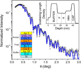
Crystalline structure was determined using X-ray diffraction. Diffraction profiles were measured in the Bragg-Brentano geometry and analysis of the diffraction profiles indicates that the Au buffers show a strong (111) texture since only the (111) and (222) peaks were visible. The width of diffraction lines are 0.7 deg, 1 deg, for the free Py/Co layer and IrMn, respectively. For the 10 and 40 nm thick Au buffer, the width is 1.1 deg and 0.4 deg, respectively. Using the Scherrer formula we estimate crystallite size as 9, 25 nm for the 10 and 40 nm Au buffer, respectively. On the basis of a fitting procedure with the use of SimulReflec SimulReflec (2007) software for x-ray reflectivity data the composition profiles of a few chosen multilayers were determined as it is shown in Fig. 1, as a typical example. Thickness of the individual layers (Fig. 1, the upper inset) is in agreement with that assumed from technological parameters. The roughness estimated from the fitting is of 0.5 - 0.7 nm.
The magnetization reversals of the multilayers were examined using a standard vibrating sample magnetometer at room temperature. The measurements confirmed that the multilayers comprise the perpendicular magnetized polarizer with the effective magnetization kG, the in-plane magnetized free layer with kG, and the analyzer with kG and the exchange-bias field of 200 Oe. The individual P, F, and A magnetic layers have approximately the same magnetic moments.
III CPW VNA-FMR measurement technique
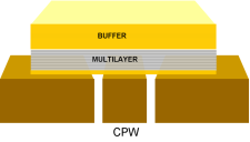
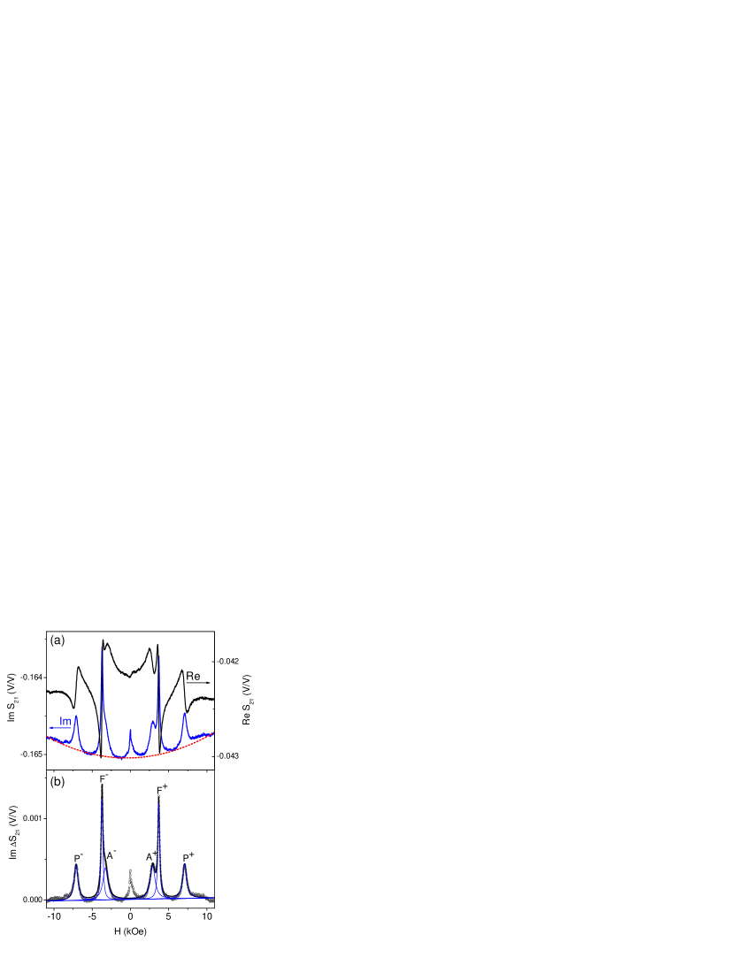
A broadband FMR spectrometer based on the VNA-FMR technique was used to measure the FMR spectra of multilayers in the in-plane geometry with an external magnetic field applied in the sample plane. An in-plane microwave field with a frequency of 20 - 30 GHz was applied to the sample using a grounded CPW with a 0.45 mm wide central strip. Our CPW design is similar to that of Southwest Microwave Inc. Rosas (2011) The samples ( mm) were placed face down on the CPW so that the buffer layer was always the furthest layer in the investigated multilayer structures as it is schematically shown in Fig. 2. The complex transmission parameter was measured with the VNA at a fixed frequency - typically 20 GHz - while the external magnetic field was swept between +10, 0, and -10 kOe. Since the FMR signals were measured in two quadrants, the number of FMR peaks is doubled as it is shown in Fig. 3. We find such a measurement procedure helpful in estimating errors in calculations of the area under absorption curve. Figure 3 (a) shows typical real part Re and imaginary part Im of a complex scattering factor S with a phase correction. Kalarickal et al. (2006) Two main features characterize Im vs. : a quasi-parabolic background Im which is related to a nonresonant background of the whole microwave track and six characteristic absorption peaks (three for positive and three for negative , respectively) plus one central peak. The three peaks P+, F+, and A+ (or, P-, F-, and A-, for the negative field direction) are related to the FMR absorption of the exchange decoupled polarizer, the free layer, and the analyzer, respectively. The central peak at Oe is related to a additional absorption due to magnetization reversal of the F+A structure. The central peak will not be discussed further in this paper.
Figure 3 (a) clearly shows that the experimental data of Im can be broken into magnetic and nonmagnetic contributions assuming that a reflection of microwave power is weak in our VNA-FMR set-up. Therefore, following a similar analysis discussed in Refs. Nembach et al., 2011; Ding, Klemmer, and Crawford, 2004, the complex scattering term may be expressed as
| (1) |
where is complex microwave susceptibility, is complex function of the experimental parameters , such as frequency and film thickness Ding, Klemmer, and Crawford (2004). Furthermore, time takes into account some drift of during measurements. Assuming that depends on in a nonresonant way and also depends on , we can reasonably approximate so that we arrive at a simple relation
| (2) |
where . Figure 3 (b) shows the measured Im ) after subtraction of the nonresonant background Im . It can be easily shown that the experimental spectrum can be deconvoluted using a set of Lorentzians. Slight differences in the height and linewidth (FWHM) for P+, P- and F+,F- peaks serve here as a rough estimate of uncertainties in determination of the absorptions in our VNA-FMR set-up. On the other hand, the substantial difference between A+ and A- is due to the unidirectional anisotropy of the analyzer. Keeping in mind that , we can further express the area under the FMR absorption peak as
| (3) |
In theory, the intensity of the FMR absorption measured in a microwave cavity is proportional the total magnetic moment.Gurevich and Melkov (1996) However, in this case the FMR intensity studies require a microwave system which can provide reproducible results with a special emphasis on a microwave cavity coupling and a cavity quality factor. Celinski, Urquhart, and Heinrich (1997) In contrast to the discussion in Ref. Harward et al., 2011, we have found the magnitude of the FMR absorption ( Im ) quite stable for the structures of the same size and the same composition. It suggests that we can compare the intensities of FMR absorption of various samples provided that the measurement conditions in the CPW set-up are the same.
IV VNA-FMR results
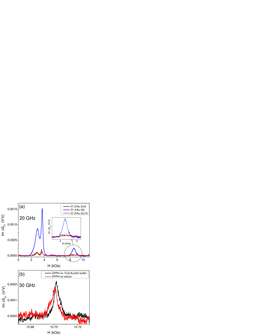
Using our CPW-VNA set-up, we have measured FMR of three SA, SA1, and SA2 structures that comprise identical P, F, and A but different buffer layers (see Tab. 1, for details). As it is shown in Fig. 4 (a), the same positions of the resonance field of the P, F, and A layers in the three structures prove that the magnetic layers have the same magnetic properties (e.a., the same values of effective magnetization and the same exchange bias of the analyzer) In contrast, the signal amplitude of Im for SA with the thickest Au buffer is nearly 6 - 7 times higher than those of SA1 and SA2. The effect of signal enhancement is even more pronounced for the polarizer P with the perpendicular anisotropy (see the inset in Fig. 4 (a)). While the FMR absorptions of the polarizer are barely seen from the noise for the samples SA1 and SA2, the FMR absorption of P in SA is substantial and comparable with those of A and F. As it was shown in our recent paper, Matczak et al. (2013) the enhancement in this case is presumably additionally influenced by a better texture and crystallite size of the polarizer, which was grown on the thick Au 40 nm buffer layer. Therefore, Fig. 4 (a) can be regarded as an experimental evidence of shielding of the electromagnetic field in the CPW by a conducting film with a low sheet resistance. It is shown that a highly conducting buffer layer that is the outer conducting layer from CPW can beneficiary affect the excitation of the fundamental mode(s) in our ultrathin film structure. We have checked with a four-point probe that the sheet resistance of SA, SA2, and SA1 buffer layers is of 0.5, 15 and 30 , respectively.
Such a change in the sheet resistance has recently been shown to strongly affect shielding of either and/or fields. Bailleul (2013) To check if the field is really enhanced due to a conducting buffer alone, we performed a similar experiment using DPPH - the common EPR standard compound - dissolved in a nonconducting glue and then deposited on a bare Si substrate and on a Si substrate covered with a Au 40 nm buffer layer, respectively. As it is shown in Fig. 4 (b), there is no substantial signal enhancement due to the thick Au buffer. Since the DPPH ”layers” are insulating and very thick (of 100 m), we attribute the FMR signal enhancement for the conducting SA, SA1, and SA2 structures to their close proximity of conducting nonmagnetic layers.
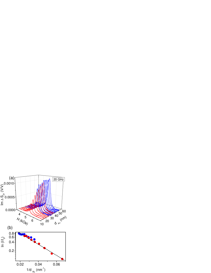
The VNA-FMR measurements of a single ultrathin Co film in contact with a wedged Au buffer give reference data for quantitative analysis. For this purpose, we measured Im for the 2.5 nm Co layer deposited on the 10 - 40 nm and Au 30 - 60 nm Au wedges (see Tab. 1). The results of the FMR measurements are shown in Fig. 5 (a) as a 3-D plot. It is clearly seen that the amplitude of the FMR absorption of the Co 2.5 nm layer increases with the thickness of Au buffer layer and saturates at its thickness of 40-60 nm. It appears that a dependence of the intensity vs. (see Fig. 5 (b)) can be approximated by the following expression:
| (4) |
where is of 38 nm and are the fitting parameters. If we define the sheet resistance of Au buffer layer as Eq. (4) can be alternatively expressed in terms of the sheet resistance. By assuming the resistivity of bulk gold as 3 cm, of the Au buffer varies from 2 to 0.33 for the Au thickness of 10 and 60 nm, respectively. Fitting to the experimental data using Eq. (4) gives .
| Sample | : | ||
|---|---|---|---|
| SA,SB,SD | 1 | 0.8 | 1.07 |
| SA - inverse structure | 1 | 0.84 | 0.97 |
| SB - simple structure | 1 | 0.86 | 0.58 |
| SD - simple structure | 1 | 0.64 | 0.40 |
Fig. 6 shows the effect of the FMR absorption enhancement observed in more complex structures SA, SB, SC, and SD that include the P, F, and A magnetic layers in various arrangements with respect to the buffer layers (Tab. 1). For some purposes, which are out of scope of the present paper, the sample SC has no polarizer. Comparing Figs. 6 (SA), (SB) with (SC), and (SD), one can see that the FMR amplitudes for the samples SA and SB deposited on the Au 40 nm buffers are about ten times higher than those of the samples SC and SD deposited onto the Au 10 nm buffers. Besides, a clear decrease in the signal-to-noise ratio is seen in Fig. 6 for SA and SB in comparison with the SC and SD structures.
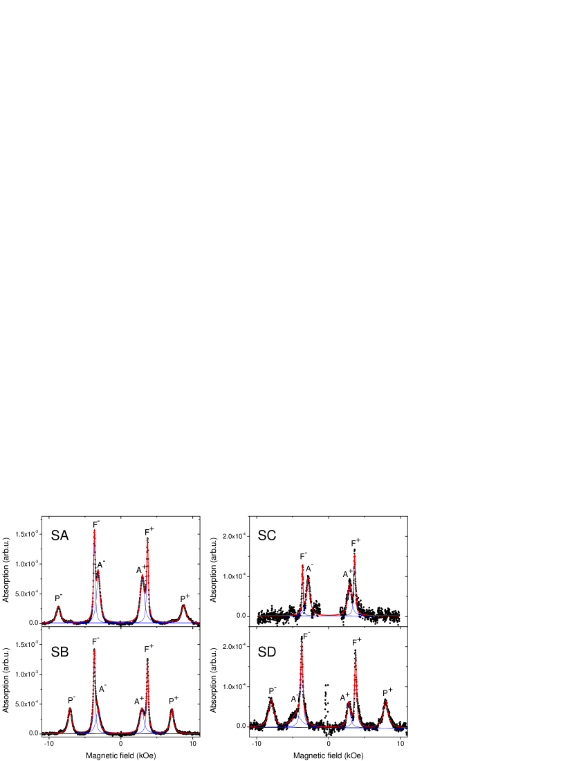
As can be seen in Tab. 1, the multilayer samples differ in sequences of the magnetic layers. The P-F-A and A-F-P structures are referred to as the simple and the inverse structures, respectively. Let us examine the impact of the arrangements of magnetic layers on their FMR intensity ratios. According to Eq. (3), the FMR intensity ratio of to to should be the same as the magnetic moments ratio (Tab. 2) provided the dynamic field is homogeneous. However, Tab. 2 shows that ratios depend on an arrangement of magnetic layers. For the simple structures SB and SD the intensity ratios are distinctly different from that of . Moreover, the intensity of FMR absorption is strongly diminished for the analyzer A with a IrMn layer in close contact with the Au buffer. On the other hand, for the inverse structure SA the FMR intensity ratio does not differ much from the ratio of the magnetic moments.
V Discussion
Discussion of our experimental data is based on the essential results of Ref. Kostylev, 2009. (i) In contrast to the common cavity FMR measurements, a conducting thin film sample in the CPW - FMR is illuminated by microwaves asymmetrically from the front surface of the film as it is shown in Fig. 7. (ii) In such a geometry, the thin film sample with a thickness less than the skin depth the microwave magnetic field decays more strongly than exponentially. (iii) In a highly conducting film the microwave magnetic field is strongly inhomogeneous.
We can write the scattering parameter in terms of the complex reflection coefficient and the complex propagation factor .Bilzer et al. (2007)
| (5) |
is the complex propagation factor of the unloaded CPW, where is the angular frequency of microwave field and is the phase velocity of microwaves in the the CPW. is the propagation index of the loaded CPW. is the film width and is the scattering parameter of the empty CPW. Keeping only linear term in the expansion of Eq. (5) and assuming that ,Kennewell et al. (2010) we obtain
| (6) |
The propagation index can be further approximated in terms of the characteristic impedance , (Eq. (13) in Ref. Kostylev, 2009), where is the characteristic impedance of the unloaded CPW and is the surface impedance of a thin film placed on the CPW. Hence,
| (7) |
According to Ref. Bailleul, 2013
| (8) |
where is the sheet resistance and is a width of the central line of CPW (see. Fig. 2 in Ref. Bailleul, 2013). Eventually, in agreement with Ref. Kostylev, 2009, we can express the measured scattering coefficient in terms of geometrical parameters of CPW and the film placed on it
| (9) |
which has the same form as the fitting formula Eq. (4) to the experimental data shown in Fig. 5. Let us estimate . For , cm-1, cm, cm/s, and GHz the estimated range of is between 8 and 15 nm if we assume the resistivity cm of the gold buffer the same as for bulk. In practice, the resistivity of several nanometers thick gold films is several times higher Sambles, Elsom, and Jarvis (1982) so that nm estimated from fitting of the experimental data (Fig. 5) according to Eq. (4) is in agreement with the above model.
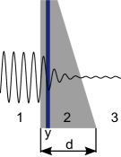
Let us consider an ultrathin Co 2.5 nm film deposited on a gold wedged buffer layer of thickness nm as it shown in Fig. 7. The Co film plays the role of a tag useful for monitoring of the dynamic magnetic field . Since the Co film is very thin in comparison to the Au buffer, we assume that the entire structure has the conductivity of gold wedge (region 2). A transverse wave with a wavenumber and with the amplitude equal to unity incidents perpendicular to the film surface from region 1 with the permittivity the same as for region 3. Kostylev (2009) The permittivity of region 2 is complex. Taking continuity boundary conditions at the boundaries of regions 1, 2, and 3 for and we have
| (10) | |||||
| (11) | |||||
| (12) |
with
| (13) | |||||
| (14) | |||||
| (15) | |||||
| (16) |
where and . Since and of gold is imaginary and very large,Kennewell et al. (2010) so that after expanding exponential functions and keeping only the linear terms of expansions we obtain that varies linearly with as
| (17) |
where 2 on the right-hand side denotes that the amplitude at the front of the structure is doubled due to the positive interference.
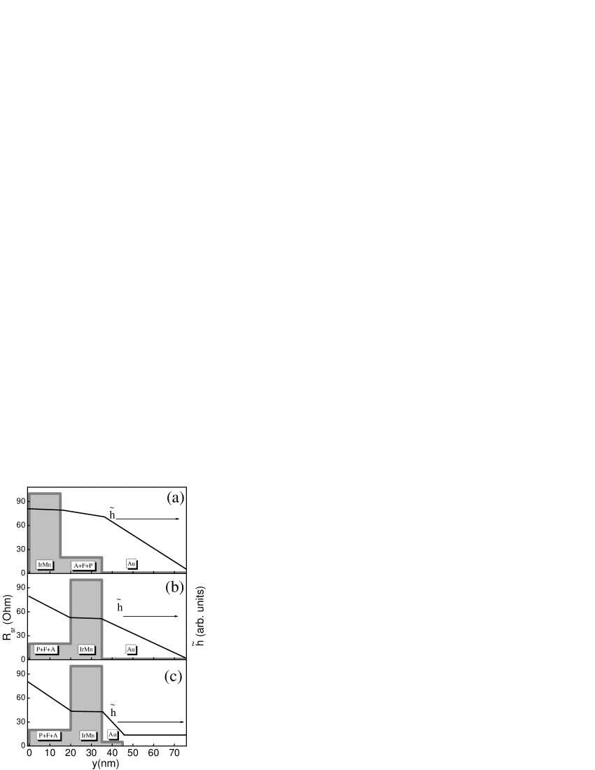
In order to extend the model of inhomogeneous dynamic magnetic field within more complicated structure that comprise P+F+A layers and the Au buffer layer, let us compare the FMR intensity of the CPW-FMR responses shown in Fig. 6. In contrast to the single ultrathin Co film on the Au buffer layer, the P+F+A ferromagnetic structure is more extended (of nm) and consists of the exchange decoupled (the Cu spacers are 3 - 4 nm thick) Co and Permalloy layers with diverse effective anisotropies. This makes possible observation of the well separated the FMR absorptions of each layer. Exact calculations of the electromagnetic field distribution in such structures would require a set of many boundary conditions Maksymov and Kostylev (2013) with several material parameters. However, we make use of Eq. (17) taking into account that in the multilayer is a linear combination of in individual layers and its slope scales with a sheet resistance () of the individual layers. Kennewell et al. (2010) Hence, the lower the higher is the slope of within a layer. values of the individual layers in the entire stack are quite diverse - is the highest for the IrMn layer Umetsu, Fukamichi, and Sakuma (2006) and the lowest for the Au buffers. Possible distributions of the dynamic field (black lines) are shown in Fig. 8 (a), (b), and (c) for SA, SB, and SD structures, respectively. In other words, we assume in accordance with Eq. (17) that and what is generally not true for very thin stacks (see Fig. 6 in Ref. Kostylev, 2009) so that the microwaves can be partially transmitted out of the stack as it is shown in Fig. 8 (c). Nonetheless, the distributions of just depict graphically that its slope in the P+F+A stacks is the highest for the SD sample and the lowest for the SA sample so that the magnetic field inside the SA sample is the most homogeneous. It is also seen that the position of antiferromagnetic IrMn pinning layer plays an important role in the distribution of because its resistivity Umetsu, Fukamichi, and Sakuma (2006) is about 100 times higher than that of Au. Sambles, Elsom, and Jarvis (1982) Hence, in accordance with the sketches shown in Fig. 8, the dynamic magnetic field is the most inhomogeneous for the SD sample with the simple P+F+A structure. In contrast, for the SA sample with the inverse A+F+P structure the FMR intensity ratio is in a fairly good agreement with the ratio of magnetic moments estimated from geometry of P, F, and A layers.
VI Conclusions
We have expanded former Counil et al. (2004); Neudecker et al. (2006); Bilzer et al. (2007); Harward et al. (2011); Kennewell et al. (2010); Nembach et al. (2011); Ding, Klemmer, and Crawford (2004); Kennewell, Kostylev, and Stamps (2007); Crew et al. (2005); Kostylev (2009) coplanar waveguide based VNA-FMR studies of thin magnetic films to ultrathin magnetic structures deposited on the buffer layers with diverse sheet resistance . We showed that the intensity of the FMR absorption of the single ultrathin Co layer depends on the thickness of the conducting Au buffer or, equivalently, on the buffer sheet resistance . We showed that the measured FMR absorption intensities of structures composed of several exchange decoupled ultrathin magnetic layers do not scale in proportion to their magnetic moments as would be expected. On the contrary, the ratios of FMR absorption intensity of the individual P, F, and A layers depend on their arrangement with respect of the buffer layer. The above mentioned findings are interpreted in terms of the microwave shielding effect by the conducting nonmagnetic buffers and the inhomogeneous dynamic field . The coplanar waveguides (micro-antennas) are widely used in numbers of spintronic devices Kruglyak, Demokritov, and Grundler (2014) and the enhancement of FMR response has potential to be applied in spintronic devices.
Acknowledgment
This research has been conducted in framework of Project NANOSPIN PSPB-045/2010 supported by a grant from Switzerland through Swiss contribution to the enlarged European Union. The authors thanks Dr B. Szymański for assistance with x-ray measurements, A. Krysztofik for assistance with FMR measurements, and Dr P. Balaẑ for his help with some calculations.
References
- Counil et al. (2004) G. Counil, J.-V. Kim, T. Devolder, C. Chappert, K. Shigeto, and Y. Otani, J. Appl. Phys. 95 (2004).
- Neudecker et al. (2006) I. Neudecker, G. Woltersdorf, B. Heinrich, T. Okuno, G. Gubbiotti, and C. Back, J. Magn. Magn. Mater. 307, 148 (2006).
- Bilzer et al. (2007) C. Bilzer, T. Devolder, P. Crozat, C. Chappert, S. Cardoso, and P. Freitas, J. Appl. Phys. 101, 074505 (2007).
- Harward et al. (2011) I. Harward, T. O’Keevan, A. Hutchison, V. Zagorodnii, and Z. Celinski, Rev. Sci. Instr. 82, 095115 (2011).
- Kennewell et al. (2010) K. J. Kennewell, M. Kostylev, N. Ross, R. Magaraggia, R. L. Stamps, M. Ali, A. A. Stashkevich, D. Greig, and B. J. Hickey, J. Appl. Phys. 108, 073917 (2010).
- Nembach et al. (2011) H. T. Nembach, T. J. Silva, J. M. Shaw, M. L. Schneider, M. J. Carey, S. Maat, and J. R. Childress, Phys. Rev. B 84, 054424 (2011).
- Ding, Klemmer, and Crawford (2004) Y. Ding, T. Klemmer, and T. Crawford, J. Appl. Phys. 96, 2969 (2004).
- Heinrich and Bland (2005) B. Heinrich and J. C. Bland, Ultrathin Magnetic Structures II (Springer Berlin Heidelberg, 2005) pp. 195–296.
- Celinski, Urquhart, and Heinrich (1997) Z. Celinski, K. Urquhart, and B. Heinrich, J. Magn. Magn. Mater. 166, 6 (1997).
- Kennewell, Kostylev, and Stamps (2007) K. J. Kennewell, M. Kostylev, and R. L. Stamps, J. Appl. Phys. 101, 09D107 (2007).
- Bailleul (2013) M. Bailleul, Appl. Phys. Lett. 103, 192405 (2013).
- Nibarger, Lopusnik, and Silva (2003) J. P. Nibarger, R. Lopusnik, and T. J. Silva, Appl. Phys. Lett. 82, 2112 (2003).
- Crew et al. (2005) D. C. Crew, K. J. Kennewell, M. J. Lwin, R. C. Woodward, S. Prasad, and R. L. Stamps, J. Appl. Phys. 97, 10A707 (2005).
- Kostylev (2009) M. Kostylev, J. Appl. Phys. 106, 043903 (2009).
- Maksymov and Kostylev (2013) I. S. Maksymov and M. Kostylev, J. Appl. Phys. 113, 043927 (2013).
- Houssameddine et al. (2007) D. Houssameddine, U. Ebels, B. Delaët, B. Rodmacq, I. Firastrau, F. Ponthenier, M. Brunet, C. Thirion, J.-P. Michel, L. Prejbeanu-Buda, et al., Nature materials 6, 447 (2007).
- SimulReflec (2007) SimulReflec, “Lab. Leon Brillouin CEA/CNRS UMR12,” (2007), http://www-llb.cea.fr/prism/programs/simulreflec/simulreflec.
- Rosas (2011) B. Rosas, “The Design and Test of Broadband Launches up to 50 GHz on Thin and Thick Substrates,” (2011), http://mpd.southwestmicrowave.com/resources/.
- Kalarickal et al. (2006) S. S. Kalarickal, P. Krivosik, M. Wu, C. E. Patton, M. L. Schneider, P. Kabos, T. J. Silva, and J. P. Nibarger, J. Appl. Phys. 99, 093909 (2006).
- Gurevich and Melkov (1996) A. Gurevich and G. Melkov, Magnetization Oscillations and Waves (CRC Press, 1996).
- Matczak et al. (2013) M. Matczak, B. Szymański, M. Urbaniak, M. Nowicki, H. Głowiński, P. Kuświk, M. Schmidt, J. Aleksiejew, J. Dubowik, and F. Stobiecki, J. Appl. Phys. 114, 093911 (2013).
- Sambles, Elsom, and Jarvis (1982) J. R. Sambles, K. C. Elsom, and D. J. Jarvis, Phil. Trans. of the Royal Soc. of London A 304, 365 (1982).
- Umetsu, Fukamichi, and Sakuma (2006) R. Y. Umetsu, K. Fukamichi, and A. Sakuma, Mater. Trans. 47, 2 (2006).
- Kruglyak, Demokritov, and Grundler (2014) V. V. Kruglyak, S. O. Demokritov, and D. Grundler, J. Appl. Phys. 115, 043917 (2014).