CO Tip Functionalization Inverts Atomic Force Microscopy Contrast via Short-Range Electrostatic Forces
Abstract
We investigated insulating Cu2N islands grown on Cu(100) by means of combined scanning tunneling microscopy and atomic force microscopy with two vastly different tips: a bare metal tip and a CO-terminated tip. We use scanning tunneling microscopy data as proposed by Choi et al. Choi et al. (2008) to unambiguously identify atomic positions. Atomic force microscopy images taken with the two different tips show an inverted contrast over Cu2N. The observed force contrast can be explained with an electrostatic model, where the two tips have dipole moments of opposite directions. This highlights the importance of short-range electrostatic forces in the formation of atomic contrast on polar surfaces in non-contact atomic force microscopy.
The combination of scanning tunneling microscopy (STM) with non-contact atomic force microscopy (NC-AFM) in a single probe enables a wide range of atomic scale studies on surfaces. Whereas contrast mechanisms in STM for different tip-sample systems are widely understood, interpretation of NC-AFM data remains challenging. In NC-AFM the sum over all tip-sample interactions is measured, and the source of atomic resolution is often hard to identify. On semiconductors Pérez et al. (1997), as well as on metals Dieška et al. (2003), imaged with reactive tips (e.g. Si) atomic contrast is dominated by the formation of covalent bonds that often reach magnitudes of nanonewtons. For non-reactive CO functionalized tips, Pauli repulsion was attributed to the observed intermolecular resolution Gross et al. (2009a); Moll et al. (2010). Lantz et al. Lantz et al. (2003) showed that the dangling bonds of Si(111) 77 can induce a dipole moment in (non-reactive) oxidized Si tips resulting in a short-range electrostatic interaction, which contributes to atomic resolution. Electrostatic interaction and an induced tip dipole moment was also used to explain atomic contrast on ionic crystals Giessibl (1992). A similar model describes the interaction with charged adatoms on thin insulating layers Gross et al. (2009b); Bocquet et al. (2011). Moreover, it was found that clean metallic tips carry an intrinsic dipole moment Teobaldi et al. (2011); Trevethan et al. (2012), which is caused by the Smoluchowski-effect Smoluchowski (1941). All of these examples underline the importance of atomic scale electrostatic interactions in NC-AFM.
Electrostatic forces become even more meaningful as polar thin insulating layers (e.g. NaCl, MgO, Cu2N) are used to decouple adsorbates in STM and AFM experiments Repp et al. (2004, 2005); Gross et al. (2009a, b); Sterrer et al. (2007); Hirjibehedin et al. (2006); Loth et al. (2010). In this study we explore the influence of electrostatic forces in NC-AFM on Cu2N islands on Cu(100). N and Cu atoms on Cu2N form a periodic charge arrangement, as calculated by DFT Hirjibehedin et al. (2007) (Figs. 1c-e). Compared to alkali halides, the Cu2N’s c(22) unit cell structure has a lower symmetry, thus its atomic positions are easier to designate. STM experiments led to two criteria to locate N atoms within the islands Choi et al. (2008): First, N adsorbs on the hollow sites of Cu(100) Leibsle et al. (1994); Yoshimoto and Tsuneyuki (2002); Soon et al. (2008) and should therefore appear fourfold symmetric. Second, island boundaries and sharp edges are determined by N atoms Hirjibehedin et al. (2006). With this, N-, Cu- and hollow sites can be identified in the Cu2N unit cell (Fig. 1c).
In this Letter, we report on high-resolution simultaneously recorded current and force data of the Cu2N surface. We compare interaction forces probed with a CO terminated tip to data acquired with a metal tip. The force contrast, though, is inverted. We propose an electrostatic model where the two tips have opposite dipole moments. The calculated force contrast within a Cu2N unit cell provides good agreement to the data.
All experiments were carried out with a home-built low-temperature system at 6 K using a qPlus sensor ( Hz, Nm-1) Giessibl (2000) equipped with a W tip, operated with small amplitudes (50 pm) in frequency modulation mode. Metallic (Cu) tips were prepared by strongly poking them into a clean Cu sample while applying 200 V. Tips were functionalized with CO molecules following the standard procedure Bartels et al. (1997). Cu2N islands were prepared by sputtering a clean Cu(100) crystal with N gas for 120 s and heating it to 600 K for 300 s. Forces were calculated by applying the Sader-Jarvis-deconvolution method Sader and Jarvis (2004) to our recorded 3D frequency shift maps.
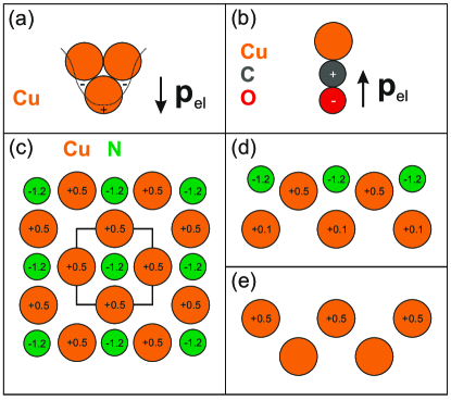
Figure 2a shows a STM topograph of an island using a Cu terminated tip recorded with a set point of 500 pA at a tip voltage of 10 mV. The image was Laplace filtered and inverted (Laplace filtering inverts brightness) to enhance contrast Hirjibehedin et al. (2006) and a structural model is partially overlaid.
When the Cu tip is terminated by a CO molecule, the STM contrast is different. The constant-current topograph in Fig. 2d was recorded using a set point of 100 pA at a tip voltage of 10 mV. Three distinct features appear within the island: elongated protrusions, wide depressions and, most remarkable, very narrow depressions. It is known that the strong p-wave character of CO terminated tips influences the imaging contrast in STM Gross et al. (2011). In Ref. Gross et al. (2011), the authors investigated the organic molecule pentacene, whose orbitals locally exhibit , and character. They use Chen’s derivative rule Chen (1993) to explain that due to the CO’s orbital the tunneling matrix element turns to zero over the pentacene’s local and orbitals, whereas not for the local orbital. We propose a similar tunneling contrast formation for copper nitride, motivated by the DFT calculations of Soon et al. Soon et al. (2008). For the eigenstate closest to our bias voltage, of 10 mV, N and Cu atoms show a local character, in which the N wave function has twice the spatial extension of Cu. Due to the 3d state of Cu and the 2p state of N, the space in between N and Cu shows a local character. Taking into account the N-Cu binding length of 183 pm, which is comparable to atomic distances within pentacene, we argue as follows: N exhibits a local character and therefore the matrix element concerning the CO’s orbital is zero, resulting in a very confined depression over N. Between N and Cu the CO tip probes a local orbital enabling a tunneling current. Cu also has local character, whereby its wave function only extends half compared to N. Furthermore, Cu is located 21 pm lower than N Yoshimoto and Tsuneyuki (2002); Soon et al. (2008). From this we conclude that our microscope setup is not able to laterally resolve a depression over Cu as well, resulting in elongated protrusions centered over Cu. For hollow sites, the lateral orbital overlap between tip and sample states is insufficient to yield a non-zero tunneling matrix element, leading to a wide depression. This lattice assignment fulfills the two required assignment criteria (Figs. 2d-e).
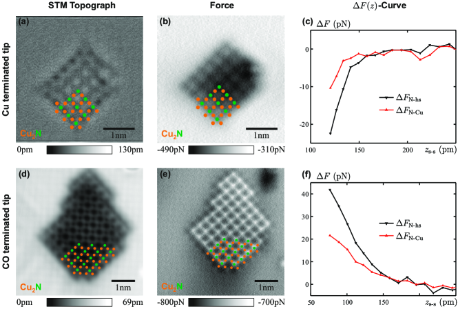
Figure 2b shows the total force for a Cu terminated tip at closest approach, corresponding to a STM set point of 28 nA at a tip voltage of 10 mV over bare Cu(100). Because the measured tunneling current is proportional to the conductance , the STM set point can be given in units of the quantum conductance ( is the elementary charge and is the Planck constant). As depends exponentially on the tip-sample distance with decay constant , can be used to calculate the distance between the front most metallic tip and sample atom, with Ternes et al. (2008). This calculation yields a lower boundary for the tip-sample distance, as typically more than two atoms contribute to the measured tunneling current SM . Here, tip-sample distance is defined as the distance between the outermost atomic shells of the involved atoms, in the following called . Using this definition of distance, Fig. 2b was measured at pm over bare Cu(100).
According to the lattice assignment for metal tips, N sites appear most attractive, followed by Cu sites and hollow sites. The measured overall force is attractive, because of the long-range van-der-Waals interaction, which normally does not depend on lateral position and thus does not allow for atomic resolution. Subtracting the forces between distinct unit cell positions cancels out constant long-range interactions and the resulting force contrast contains site dependent short-range components only. We define and as the force difference/contrast between N and Cu sites and between N sites and hollow sites (hs). Table 1 shows the averaged force contrast for five different islands probed with different Cu terminated tips at similar tip-sample-distances. The short-range character of the atomic contrast causing interaction is reflected in the -curves displayed in Fig. 2c. The atomic contrast is maintained over a vertical range of about 100 pm.
| experiment | simulation | experiment | simulation | |
| Cu tip | (-102) pN | -12 pN | (-173) pN | -17 pN |
| CO tip | (221) pN | 26 pN | (392) pN | 34 pN |
Figure 2e shows the total force at closest approach for a CO terminated tip, which was at a STM set point of 3 nA at 10 mV over clean Cu(100). To determine the tip-sample distance the above described model has to be adapted by using the point conductance of a CO molecule on the Cu surface. Experimentally we find SM and obtain pm for the closest approach. Figure 2e reveals an inverted force contrast compared to Fig. 2b, with N atoms interacting most repulsive and hollow site most attractive. The averaged force contrast for three CO functionalized tips over three different islands at similar tip-sample-distances is depicted in Table 1. Figure 2f displays the above defined -curves, showing repulsive atomic contrast for approximately 100 pm.
The AFM images in the center column of Fig. 2 show a contrast inversion for Cu vs. CO tips. We attribute this contrast inversion to opposite dipole moments of Cu vs. CO terminated tips for two reason. First, Cu2N is a periodic arrangement of charged atoms. The electrostatic potential of such a periodic charge distribution with lattice constant decays exponentially Lennard-Jones and Dent (1928), with a decay length given by (Cu2N: pm Choi et al. (2008) and thus pm). This small decay length explains the short-range character of this electrostatic interaction (Figs. 2c,f). Second, in the following we will present an electrostatic model using a point-charge representation of sample and tip. Using the force contrast and calculated tip-sample distances from the experiment, we fitted the tip’s dipole moment to model the experimental force dependence.
From experimental Choi et al. (2008) as well as theoretical work Yoshimoto and Tsuneyuki (2002); Hirjibehedin et al. (2007); Soon et al. (2008), the structural parameters and net charges of the Cu2N’s unit cell atoms are known. The distance between N and Cu is 183 pm, N atoms are vertically displaced by 21 pm with respect to the Cu surface layer and the charged subsurface Cu layer has 197 pm distance to the Cu surface layer, as indicated in Figs. 1c-e. Charges were calculated by DFT in Ref. Hirjibehedin et al. (2007) and are given by -1.2 e for N, +0.5 e for surface Cu atoms and +0.1 e for the subsurface Cu (Figs. 1c-e). Using these numbers, we constructed a 3D point-charge representation of the sample with a size of unit cells, including the subsurface Cu atoms, where all charges are located at the atomic core positions. The resulting electric field was then used to calculate the interaction force with the tip SM . The Smoluchowski effect Smoluchowski (1941) causes a charge redistribution on corrugated metal surfaces, which leads to the formation of electric dipoles. For metallic tips, an electric dipole moment is formed pointing towards the sample Teobaldi et al. (2011), as depicted in Fig. 1a. For a CO molecule adsorbed on a metal tip, the electric dipole moment compared to gas phase changes in magnitude and sign due to charge transfer to the metal. We recently found experimental Welker and Giessibl (2012); Hofmann et al. (2014) evidence that the CO’s dipole moment is pointing into the metal, as depicted in Fig. 1b, which is also supported by some ab initio molecular orbital calculations Pavão et al. (1991). The tip was modeled as a simple dipole having two charges separated by the dipole distance .
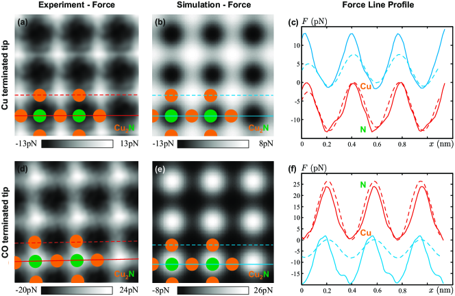
For Cu terminated tip, we got the best agreement with a charge of 0.13 e and pm (close to the atomic radius of Cu) resulting in a dipole moment of D. The dipole points towards the sample, as described before, where the positive charge is located at the core of the front most Cu tip atom. For the calculation, the positive tip charge (Cu core) was placed at a distance of 395 pm over the charges (cores) of the Cu surface layer. This distance was obtained by adding twice the atomic radius of Cu to the experimental pm SM . Figure 3b shows the calculated force between this metal tip dipole and all surface atoms. The force above the Cu site was set to zero to emphasize the force contrast. Line profiles along the N-Cu-N and Cu-hollow site-Cu direction from Fig. 3b are plotted in Fig. 3c (blue). The relative interaction contrast is given in Table 1 and fits well to the experimental results. To compare the simulation to the experiment, Fig. 3a shows a zoom-in of the island in Fig. 2b (unit cell average over the inner part plus Gauss filter) with the respective line profiles in Fig. 3c (red).
We modeled the CO tip as a dipole pointing away from the sample, where the negative charge sits at the O core and positive charge at the C core. With the CO binding length of 115 pm as dipole distance and a charge of 0.03 e the dipole moment is D. The distance of the O core to the charges of the Cu surface layer was 275 pm ( pm plus atomic radii of O, 60 pm, and Cu, 135 pm) SM . In Fig. 3e, the calculated force is shown, with the force at the Cu site set to zero. Corresponding line profiles along the two prominent direction are given in Fig. 3f (blue lines). Also, this simulation gives quantitative agreement to our experimental force contrast (Table 1). For comparison Fig. 3d shows a zoom-in of Fig. 2e (unit cell average over the inner part plus Gauss filter), with the corresponding line profiles shown in Fig. 3f.
This straight-forward electrostatic model reproduces the relative force contrast of both tip terminations very well. The experimentally determined dipole moment of the Cu terminated tip of 0.874 D is close to the range of previous work for Cr and W tips Teobaldi et al. (2011); Trevethan et al. (2012). Simulation and experiment for the CO terminated tip agree with the theory that the dipole moment points away from the sample. In general the CO’s dipole magnitude depends on the chemical nature and geometric structure of the adsorbent Pavão et al. (1991). Hence, it is not surprising that the fitted value of 0.166 D varies from CO molecules adsorbed on surfaces Feng et al. (2011); Welker and Giessibl (2012); Hofmann et al. (2014).
The simulation does not account for (attractive) covalent bonds (Cu tips) and Pauli repulsion (CO tips). Both interactions are probably included in the measured overall force and would influence the force contrast and therefore the modeled dipole moment. However, the experimental core-core distances are just a lower boundary (Cu tip: 395 pm and CO tip: 275 pm) and are so large that we don’t expect a strong contribution neither from covalent bonds nor from Pauli repulsion.
In conclusion, we have shown that atomic resolution on relatively inert surfaces such as Cu2N can also be obtained by electrostatic multipole forces, not just by covalent bonding forces or Pauli repulsion forces. Richard Feynman already pointed out in his 1939 paper Feynman (1939) that intermolecular forces ultimately have an electrostatic origin. The difference we observed here to the covalent case in atomic imaging of semiconductors is that covalent bonds usually result in massive rearrangements of electronic charge density and subsequently forces in the nanonewton regime, while the forces here are only tens of piconewtons with much less redistribution of electronic charge.
Acknowledgements.
The authors thank the Deutsche Forschungsgemeinschaft for funding within the SFB 689.References
- Choi et al. (2008) T. Choi, C. D. Ruggiero, and J. A. Gupta, Physical Review B 78, 035430 (2008).
- Pérez et al. (1997) R. Pérez, M. C. Payne, I. Štich, and K. Terakura, Physical Review Letters 78, 678 (1997).
- Dieška et al. (2003) P. Dieška, I. Štich, and R. Pérez, Physical Review Letters 91, 216401 (2003).
- Gross et al. (2009a) L. Gross, F. Mohn, N. Moll, P. Liljeroth, and G. Meyer, Science 325, 1110 (2009a).
- Moll et al. (2010) N. Moll, L. Gross, F. Mohn, A. Curioni, and G. Meyer, New Journal of Physics 12, 125020 (2010).
- Lantz et al. (2003) M. A. Lantz, H. J. Hug, R. Hoffmann, S. Martin, A. Baratoff, and H.-J. Güntherodt, Physical Review B 68, 035324 (2003).
- Giessibl (1992) F. J. Giessibl, Physical Review B 45, 13815 (1992).
- Gross et al. (2009b) L. Gross, F. Mohn, P. Liljeroth, J. Repp, F. J. Giessibl, and G. Meyer, Science 324, 1428 (2009b).
- Bocquet et al. (2011) F. Bocquet, L. Nony, and C. Loppacher, Physical Review B 83, 035411 (2011).
- Teobaldi et al. (2011) G. Teobaldi, K. Lämmle, T. Trevethan, M. Watkins, A. Schwarz, R. Wiesendanger, and A. L. Shluger, Physical Review Letters 106, 216102 (2011).
- Trevethan et al. (2012) T. Trevethan, M. Watkins, and A. L. Shluger, Beilstein Journal of Nanotechnology 3, 329 (2012).
- Smoluchowski (1941) R. Smoluchowski, Physical Review 60, 661 (1941).
- Repp et al. (2004) J. Repp, G. Meyer, F. E. Olsson, and M. Persson, Science 305, 493 (2004).
- Repp et al. (2005) J. Repp, G. Meyer, S. M. Stojković, A. Gourdon, and C. Joachim, Physical Review Letters 94, 026803 (2005).
- Sterrer et al. (2007) M. Sterrer, T. Risse, U. Martinez Pozzoni, L. Giordano, M. Heyde, H.-P. Rust, G. Pacchioni, and H.-J. Freund, Physical Review Letters 98, 096107 (2007).
- Hirjibehedin et al. (2006) C. F. Hirjibehedin, C. P. Lutz, and A. J. Heinrich, Science 312, 1021 (2006).
- Loth et al. (2010) S. Loth, K. von Bergmann, M. Ternes, A. F. Otte, C. P. Lutz, and A. J. Heinrich, Nature Physics 6, 340 (2010).
- Hirjibehedin et al. (2007) C. F. Hirjibehedin, C.-Y. Lin, A. F. Otte, M. Ternes, C. P. Lutz, B. A. Jones, and A. J. Heinrich, Science 317, 1199 (2007).
- Leibsle et al. (1994) F. M. Leibsle, S. S. Dhesi, S. D. Barrett, and A. W. Robinson, Surface Science 317, 309 (1994).
- Yoshimoto and Tsuneyuki (2002) Y. Yoshimoto and S. Tsuneyuki, Surface Science 514, 200 (2002).
- Soon et al. (2008) A. Soon, L. Wong, B. Delley, and C. Stampfl, Physical Review B 77, 125423 (2008).
- Giessibl (2000) F. J. Giessibl, Applied Physics Letters 76, 1470 (2000).
- Bartels et al. (1997) L. Bartels, G. Meyer, and K.-H. Rieder, Applied Physics Letters 71, 213 (1997).
- Sader and Jarvis (2004) J. E. Sader and S. P. Jarvis, Applied Physics Letters 84, 1801 (2004).
- Gross et al. (2011) L. Gross, N. Moll, F. Mohn, A. Curioni, G. Meyer, F. Hanke, and M. Persson, Physical Review Letters 107, 086101 (2011).
- Chen (1993) C. J. Chen, Introduction to Scanning Tunneling Microscopy (Oxford University Press, New York, 1993).
- Ternes et al. (2008) M. Ternes, C. P. Lutz, C. F. Hirjibehedin, F. J. Giessibl, and A. J. Heinrich, Science 319, 1066 (2008).
- (28) See Supplemental Material for the estimation of the error in the calculated tip-sample distance for metal tips, determination of the tip-sample distance for CO terminated tips and details for the electrostatic simulation.
- Lennard-Jones and Dent (1928) J. E. Lennard-Jones and B. M. Dent, Transactions of the Faraday Society 24, 92 (1928).
- Welker and Giessibl (2012) J. Welker and F. J. Giessibl, Science 336, 444 (2012).
- Hofmann et al. (2014) T. Hofmann, F. Pielmeier, and F. J. Giessibl, Physical Review Letters 112, 066101 (2014).
- Pavão et al. (1991) A. C. Pavão, M. Braga, C. A. Taft, B. L. Hammond, and W. A. Lester, Jr., Physical Review B 43, 6962 (1991).
- Feng et al. (2011) M. Feng, P. Cabrera-Sanfelix, C. Lin, A. Arnau, D. Sánchez-Portal, J. Zhao, P. M. Echenique, and H. Petek, ACS Nano 5, 8877 (2011).
- Feynman (1939) R. P. Feynman, Physical Review 56, 340 (1939).
![[Uncaptioned image]](/html/1402.5246/assets/x4.png)
![[Uncaptioned image]](/html/1402.5246/assets/x5.png)
![[Uncaptioned image]](/html/1402.5246/assets/x6.png)
![[Uncaptioned image]](/html/1402.5246/assets/x7.png)