Thermoelectric performance in electron and hole doped PtSb2
Abstract
We employ density functional theory to investigate the thermoelectric properties of electron and hole doped PtSb2. Our results show that for doping of 0.04 holes per unit cell (1.5 cm-3) PtSb2 shows a high Seebeck coefficient at room temperature, which can also be achieved at other temperatures by controlling the carrier concentration (both electron and hole). The electrical conductivity becomes temperature independent when the doping exceeds about 0.20 electrons/holes per unit cell. The figure of merit at 800 K in electron and hole doped PtSb2 is 0.13 and 0.21, respectively. The thermoelectric efficiency with same host material are predicted for certain doping levels.
I Introduction
Efficient room-temperature thermoelectric materials are currently a striking challenge for researchers. In general, the efficiency is determined by the figure of merit , where is the electrical conductivity, is the Seebeck coefficient, is the temperature, and is the thermal conductivity. To achieve a high , and should be large while at the same time should be small. However, increasing by increasing the carrier concentration usually decreases and increases . Therefore, it is a prime task to control the numerator (the power factor) and the denominator independently.
Kuroki have shown that a metal with pudding mold type bands (a dispersive portion and a flat portion) can exhibit good thermoelectric properties Kuroki . Recently, such bands have been reported in the cubic pyrite material PtSb2, which has a high VK-1 Nishikubo . Bulk PtSb2 can be both metallic and semiconducting for deviations from the ideal stoichiometry and it can be n- and p-type doped with charge carrier concentrations spanning several orders of magnitude (1016 cm-3 to 1020 cm-3), as observed for different synthesis methods and parameters Damon ; Elliott ; Abdullaev ; Dargys ; Laudise ; Nikolic . While -type PtSb2 (by Ir doping on the Pt site) gives a high metallic conductivity and large Seebeck coefficient Nishikubo , -type PtSb2 (by Sb deficiency) gives a large Seebeck coefficient and thermal conductivity between 0 and 300 K Sondergaard . PtSb2 has a high mobility due to the small difference in the electronegativities of Pt and Sb (2.28 and 2.05, respectively) Slack .
Thermoelectric device performance relies directly on the temperature difference and the intrinsic material parameter . For a thermoelectric generator, the thermoelectric efficiency is defined by the Carnot efficiency and the figure of merit as
| (1) |
where and are the temperatures of the hot and cold ends of the device and . The figure of merit of a thermoelectric device is
| (2) |
where and represent hole and electron doping, respectively.
The term varies with the average temperature, indicating that an increasing efficiency requires both a high and a large . Thermoelectric devices currently available reach and operate at an efficiency of 5 to 6 Sootsman . By increasing the figure of merit by a factor of 4 (depending on T) the predicted efficiency increases to 30, a highly attractive prospect. Different host materials have different work functions, , they have different potential barriers and resistances at the metal contact in the thermocouple, which affects the mobility of the carriers. Therefore, it is advantageous to use the same material for the electron and hole doped regions. In this respect, doped PtSb2 is a promising thermoelectric material with bipolar conduction. In the present work, we address the effect of electron and hole doping in PtSb which has a melting temperature of 1500 K Damon2 on and from 300 K to 800 K. We study the power factor and the figure of merit for both types of doping. We also calculate the thermoelectric generator efficiency by Eqs. (1) and (2). Our calculations demonstrate excellent materials properties for doped PtSb2.
II computational method
We calculate the band structure of PtSb2 using density function theory as implemented in the WIEN2k package wien2k . The popular generalized gradient approximation GGA is employed to optimize the volume and the internal atomic coordinates. To simulate doping, we use the virtual crystal approximation VCA and rigid band approach RBA1 ; RBA2 . This approximation is widely employed in calculations of transport properties of doped semiconductors and is accurate when the doping is not too large. After having reached self-consistency in the calculations, we employ the post-processing BoltzTraP code BoltzTraP to calculate the thermopower. This tool has demonstrated quantitative accuracy in calculating the thermopower of metals and doped semiconductors Madson ; Scheidemantel ; Singh ; Zhang . We use 3000 k-points in the full Brillouin zone for calculating the electronic structure and a dense mesh of 3564 k-points in the irreducible Brillouin zone for the thermoelectric calculations. PtSb2 crystallizes in a cubic pyrite structure with space group and therefore exhibite isotropic transport properties. Our optimized lattice constant is 6.47 Å which is close to the experiment value of 6.44 Å Brese .
III Results and discussion
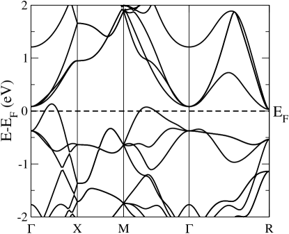
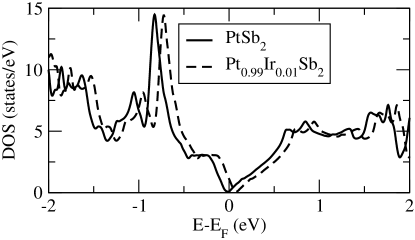
The metallic states are reproduced by our band structure calculations for Pt0.99Ir0.01Sb2 Fig. 1, while the undoped PtSb2 is an insulator with experimental gap of 110 meV at T10 K Reynolds , already a small doping of 0.04 holes per unit cell resulting in a metallic state Nishikubo . similarly, for a small -doping also results in a metallic state Sondergaard . The bands near the Fermi energy () mainly are due to the Sb 5 orbitals, with some admixtures of the Pt 5 orbitals. The band crosses the originates completely from the Sb 5 orbitals across the symmetry lines -X-M-. Mori Mori have shown that bands at are corrugated bands and not the pudding mold type bands which establish the high Seebeck coefficients in NaxCoO2 pudding and KxRhO2 krho . Calculated densities of state (DOS) of PtSb2 and Pt0.99Ir0.01Sb2 are shown in Fig. 2. It is clearly visible that doping does not change the shape of the DOS but only the position of .
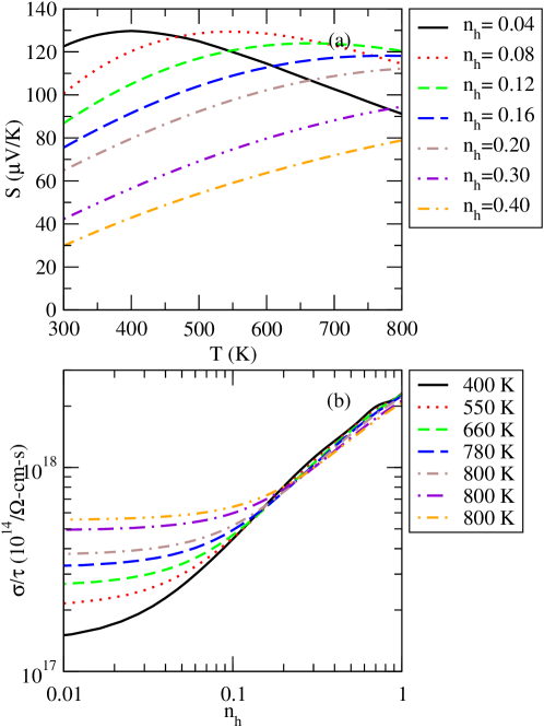
The calculated Seebeck coefficient of PtSb2 in a doping range from 0.04 to 0.40 electrons/holes per unit cell for the temperature range from 300 to 800 K is plotted in Fig. 3(a)/4(a). Note that a doping of 0.04 electrons/holes per unit cell is equivalent to a carrier concentration of 1.51020 cm-3 (as obtained experimentally for Pt0.99Ir0.01Sb2 Nishikubo ). We find that shows a maximum of above 100 V/K for each level of doping except for doping 0.3 and 0.4 electrons/holes per unit cell, but at different temperature. This maximum is due to the fact that the conduction band close to gives a negative contribution to the Seebeck coefficient at different temperatures and doping levels.
For holes per unit cell our calculation gives at room temperature a value of V/K, which is in agreement with the experiment (100 V/K) Nishikubo . Our maximum value is 129.7 V/K, while the experimental value is 112 V/K at 400 K. At doping, remains high upto 450 K, decrease thereafter. Overall Fig. 3(a) shows that with increasing hole doping the Seebeck coefficient decreases at room temperature, which is also consistent with the experiment. Importantly, the maximum value can be obtained at different temperatures by controlling the carrier concentration, which helps to achieve an optimal performance of the thermoelectric device under different conditions. In Fig. 3(b) we examine the effect of hole doping on the electrical conductivity at room temperature and of the temperatures for which we have obtained the highest for each doping. We find variations with the temperature in the case of low doping, with the highest value at 800 K. For the value of increases rapidly and becomes virtually identical for the considered temperatures. Due to a sharp increase in , is reduced for high doping.
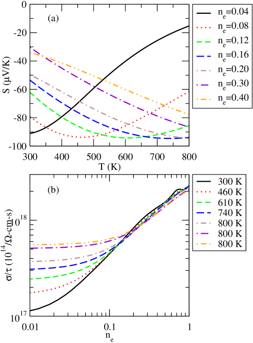
As it is experimentally known that both types of doping are possible in PtSb2, we also consider electron doping, which has not been addressed experimentally. Nishikubo Nishikubo have shown that the substitution of Sn at the Sb site results in a small power factor. This suggests that substitution at the Pt site is more favorable for the transport properties. Hence, we study substitution of Au at the Pt site, see Fig. 4(a,b). At the room temperature for 0.04, 0.12, and 0.40, is 91 V/K, 62 V/K, and 34 V/K, respectively. This decreasing trend of with increasing doping at room temperature is similar to hole doping. The maximum is always found around 94 V/K except for 0.3 and 0.4 under the consider temperature range and shifts more and more to higher temperatures with increasing doping. The variation of with the electron concentration with the temperature is similar to the case of hole doping.
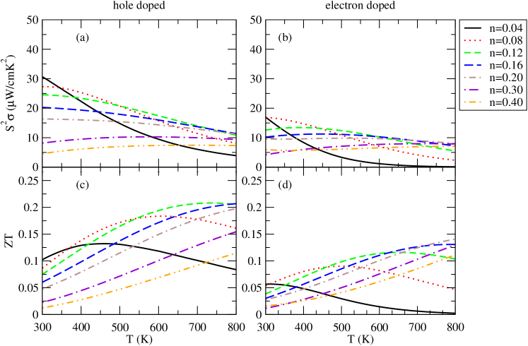
It is fruitful to compare electron and hole doping in PtSb2 for possible applications in thermoelectric generators with same host material as electron and hole conduction. In Fig. 5(a,b,c,d) we present the and of doped PtSb2, with doping range from 0.04-0.40 electrons/holes per unit cell and temperature between 300 K and 800 K. For more realistic contribution of conductivity, we vary mobility with respect to carrier concentration and temperature. Whereas the electronic contribution deduce from Wiedemann-Franz relation and phonon contribution take from experiment and vary as . Details of methodology can be found in Ref.pbse . In Fig. 5(a), the calculated room temperature for is 31 W/cmK2 in excellent agreement with the experimental value of 35 W/cmK2. For all other doping, values follow the trend of experiment at room temperature, decreases with temperature. In case of electron doped PtSb2, is reaches upto 17 W/cmK2 for lower doping which half of the hole doped PtSb2, while at higher doping electron and hole doped PtSb2 have the same magnitude of at room temperature. Importantly, behavior changes inversely with temperature for doping level 0.04 electron/hole per unit cell with respect to other doping levels. While the experiment report the power factor only for x = 0.01 above 300 K. Room temperature for doping of 0.04 holes per unit cell is above 0.1 which is in good agreement with the experimental value of 0.12. Hence, we believe our calculated results at higher temperature will also be correct. Doping between 0.120.20 electron/hole per unit cell in PtSb2, a large at 800 K results in a high ZT of around 0.10 and 0.20, respectively, which is more than double than the room temperature values of . In order to further increase by reducing thermal conductivity, a nano structure PtSb2 could be a better choice for thermoelectric devices.
Having the same host material with different types of doping joint in a device a high efficiency can be expected because of low losses at the thermal contact. This implies that PtSb2 is a good candidate for thermoelectrics. We estimate the thermoelectric device efficiency of doped PtSb2 at K, K ( K) for 0.08, 0.12 and 0.16, which shows high at . For K we obtain thermoelectric generator efficiency of 1.07, 0.82 and 0.62 for doping 0.08, 0.12 and 0.16, respectively. This efficiency could be increased by As alloying at Sb site, by reducing the thermal conductivity and by increasing Seebeck (by increasing the band gap).
IV Conclusion
To conclude, we have studied the transport properties of electron and hole doped PtSb2 over a wide doping range, using first principles calculations. A doping of 0.04 electrons/holes per unit cell gives a high power factor at room temperature, which decreases further with increasing temperature. Our results show that doping between 0.120.20 electrons/holes per unit cell, the are more than double achieved at 800 K due to a high electrical conductivity. Experiments should be performed at this doping level and temperature range for confirmation. We have demonstrated that the highest Seebeck coefficient is obtained at different temperatures for different doping levels. This allows to optimize thermoelectric devices operated at different temperatures by tuning the carrier concentration. We also calculate thermoelectric generator efficiency for certain doping levels. Moreover, it will be desirable to study in more detail about nano structure doped PtSb2 to further reduce thermal conductivity.
References
- (1) K. Kuroki and R. Arita, J. Phys. Soc. Jpn. 76, 083707 (2007).
- (2) Y. Nishikubo, S. Nakano, K. Kudo, and M. Nohara, Appl. Phys. Lett. 100, 252104 (2012).
- (3) D. H. Damon, R. C. Miller, and P. R. Emtage, Phys. Rev. B 5, 2175 (1972).
- (4) C. T. Elliott and S. E. R. Hiscocks, J. Mater. Sci. 3, 174 (1968).
- (5) A. A. Abdullaev, L. A. Angelova, V. K. Kuznetsov, A. B. Ormont, and Y. I. Pashintsev, Phys. Stat. Sol. A 21, 339 (1974).
- (6) A. Dargys and J. Kundrotas, J. Phys. Chem. Solids 44, 261 (1983).
- (7) R. A. Laudise, W. A. Sunder, R. L. Barns, G. W. Kammlott, A. F. Witt, and D. J. Carlson, J. Cryst. Growth 102, 21 (1990).
- (8) P. M. Nikolic, S. S. Vujatovic, D. M. Todorovic, M. B. Miletic, A. Golubovic, A. I. Bojicic, F. Kermendi, S. Duric, K. T. Radulovic, and J. Elazar, Jpn. J. Appl. Phys. 36, 1006 (1997).
- (9) M. Sndergaard, M. Christensen, L. Bjerg, K. A. Borup, P. Sun, F. Steglich, and B. B. Iversen, Dalton Trans. 41, 1278 (2012).
- (10) G. A. Slack, in CRC Handbook of Thermoelectrics, ed. D. M. Rowe, CRC Press, Boca Raton, page 407 (1995).
- (11) J. R. Sootsman, D. Y. Chung, and M. G. Kanatzidis, Angew. Chem. Int. Ed. 48, 8616 (2009).
- (12) D. H. Damon, R. C. Miller, and A. Sagar, Phys. Rev. 138, A636 (1965).
- (13) P. Blaha, K. Schwarz, G. Madsen, D. Kvasicka, and J. Luitz, WIEN2k, An Augmented Plane Wave + Local Orbitals Program for Calculating Crystal Properties (TU Vienna, Vienna, 2001).
- (14) J.P. Perdew, K. Burke, M. Ernzerhof, Phys. Rev. Lett. 77, 3865 (1996).
- (15) N. J. Ramer and A. M. Rappe, Phys. Rev. B 62, R743 (2000) and references therein.
- (16) L. Chaput, P. Pécheur, J. Tobola, and H. Scherrer, Phys. Rev. B 72,085126 (2005).
- (17) L. Jodin, J. Tobola, P. Pécheur, H. Scherrer, and S. Kaprzyk, Phys. Rev. B 70, 184207 (2004).
- (18) G. K. H. Madsen and D. J. Singh, Comput. Phys. Commun. 175, 67 (2006).
- (19) G. K. H. Madsen, K. Schwarz, P. Blaha, and D. J. Singh, Phys. Rev. B 68, 125212 (2003).
- (20) T. J. Scheidemantel, C. Ambrosch-Draxl, T. Thonhauser, J. V. Badding, and J. O. Sofo, Phys. Rev. B 68, 125210 (2003).
- (21) D. J. Singh, Phys. Rev. B 76, 085110 (2007).
- (22) L. Zhang, M.-H. Du, and D. J. Singh, Phys. Rev. B 81, 075117 (2010).
- (23) N. E. Brese and H. G. von Schnering, Z. Anorg. Allg. Chem. 620, 393 (1994).
- (24) R. A. Reynolds, M. J. Brau and R. A. Chapman, J. Phys. Chem. Solids 29, 755 (1968).
- (25) K. Mori, H. Usui, H. Sakakibara, and K. Kuroki, arXiv:1207.6181
- (26) K. Kuroki and R. Arita, J. Phys. Soc. Jpn. 76, 083707 (2007).
- (27) Y. Saeed, N. Singh, and U. Schwingenschlögl, Adv. Funct. Mater. 22, 2792 (2012).
- (28) D. Parker and D. J. Singh, Phys. Rev. B 82, 035204 (2010).