Size Effect on the Short Range Order in Amorphous Materials
Abstract
Drawing inspiration from nature, where some organisms can control the short range order of amorphous minerals, we successfully manipulated the short range order of amorphous alumina by surface and size effects. By utilizing the Atomic Layer Deposition (ALD) method to grow amorphous nanometrically thin films, combined with state-of-the-art electron energy loss spectroscopy (EELS) and X-ray photoelectron spectroscopy (XPS), we showed experimentally that the short range order in such films is strongly influenced by size. This phenomenon is equivalent to the well-known size effect on lattice parameters and on the relative stability of different polymorphs in crystalline materials. We also show that the short range order changes while still in the amorphous phase, before the amorphous to crystalline transformation takes place.
Many organisms use crystallization through an amorphous phase as the route for biologically controlled mineralization[1, 2]. This approach has several advantages, such as lowering the activation energy for crystal formation[3], control over the final shape of the crystal, controlled incorporation of impurities, and control over the resulting polymorph[4]. The latter is achieved by manipulation of the short range order in the amorphous phase, to resemble that of the succeeding crystalline phase[5]. This control is achieved through different additives, such as organic molecules, water, magnesium, or phosphorus[6].
This strategy used by organisms, if emulated synthetically, would have a tremendous impact, as many aspects of science and technology rely on amorphous materials[7, 8] and require specific crystalline structures in crystalline materials[9]. The crystalline structure can be controlled mainly through temperature and pressure manipulation (thermodynamics) and by epitaxial growth[10]. However, to the best of our knowledge there is no study or technology in which a polymorph has been stabilized via control of the short range order of its amorphous precursor in a non-biological system.
In our quest to emulate this biological strategy, we note the well-known feature of nanometric scale structures, namely that the influence of surface properties on the bulk is very significant[11, 12]. It was shown, for example, that size influences the lattice parameters of crystalline nanoparticles[13, 14] and changes the comparative stability of different phases[15, 16]. This occurs due to the increasing influence of surface stress and surface energy as the particle size decreases. This influence does not require the particle to be crystalline, but should be present in any solid material[17].
In the present study we investigated whether the short range order of an amorphous material can indeed be manipulated solely via size. We chose atomic layer deposition (ALD) as our material deposition method, since it is a technique that can provide extremely precise, sub-nanometric, thickness control and can deposit conformal and pinhole-free amorphous films of various materials[18]. One of the most common processes for which the ALD is used is the growth of thin, amorphous, \ceAl2O3 films, mainly for the micro- and nano-electronics industry[18]. Therefore, our material of choice in this study was amorphous alumina. An additional advantage of using \ceAl2O3 is that it has many metastable polymorphs at room temperature[19], which may also suggest an ease of switching between different short range order states.
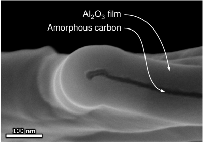
Investigating the short range order of amorphous materials is more complex than studying the crystalline structure of crystalline materials. In this study we chose to use transmission electron microscopy (TEM) and in particular the electron energy loss spectroscopy EELS method, as well as X-ray photoelectron spectroscopy (XPS), to probe the short range order. We deposited various nanometric thicknesses of amorphous alumina directly onto ‘holey’ amorphous carbon and amorphous \ceSi3N4 membrane TEM grids. After deposition the samples were transferred directly into the TEM, and EELS was performed without any further sample manipulation or preparation. An example of such a film deposited on a holey amorphous carbon membrane can be seen in Fig. 1. It is apparent that the film, as expected, is very conformal and void-free.
The deposited films were amorphous, which could be verified by electron diffractions (fig. S1). EELS reference measurements were performed on sub- powders of crystalline -\ceAl2O3 and -\ceAl2O3, at the aluminum L2,3-edge (Fig. 2A). The resulting spectra conformed well with literature reports[20, 21]. It should be noticed that a pre-edge shoulder feature at the aluminum L2,3-edge can be observed only in the case of -\ceAl2O3. This is because of the presence of 4-coordinated (tetrahedral) Al sites[20, 22], which are present only in the -\ceAl2O3 structure, and not in that of -\ceAl2O3, in which all the Al sites are rather 6-coordinated (octahedral).
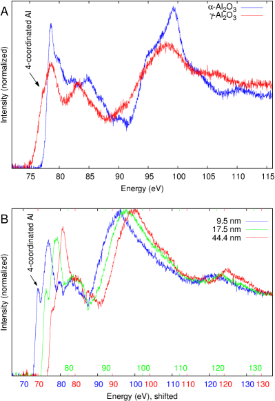
Similar measurements were performed on the ALD-deposited amorphous films of different thicknesses (Fig. 2B). A clear trend could be observed in these measurements, namely that the prominent 4-coordinated Al feature (shoulder appearance at the Al L2,3-edge) is more pronounced in the case of thinner films, whereas for the thicker ones (above approximately 20 nm) the shoulder that appears in the spectrum is much weaker. This means that thicker amorphous films demonstrate, on average, a short range order in which fewer tetrahedral Al sites are present, while thinner amorphous films demonstrate a structure richer in these sites. This finding is striking, as the only difference between these films is their thickness (deposition parameters were kept constant for all samples).
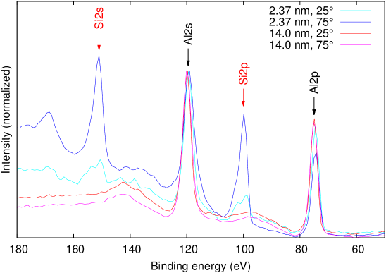
To further verify the EELS measurements, we used the XPS technique. A reference measurement was performed on the same powders of crystalline and alumina as those on which the EELS calibration measurements were performed. Fig. 3A shows the Al2p peaks acquired by this measurement. Peak broadening can be seen, as well as a slight shift towards lower energies in the case of -\ceAl2O3, relatively to the peak of -\ceAl2O3, in good agreement with the EELS results (see Fig. 2A). This is attributable to the presence in alumina of tetrahedral Al sites, which have lower binding energy than the octahedral Al sites[23, 24].
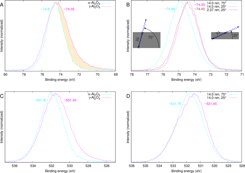
To investigate the size effect on amorphous thin films we had to take into consideration that in contrast to the EELS method, in which the signal originates from the entire sample thickness, in XPS the signal originates only from the top several nanometers below the surface. We therefore performed angle-resolved XPS (ARXPS), which enabled us to analyze the sample with depth resolution, by sampling photoelectrons from different takeoff angles. The sampling depth from which 95% of the signal intensity in ARXPS comes can be roughly estimated as , where is the attenuation length for photoelectrons in the sample, and is the takeoff angle of the photoelectrons[25]. Thus, the sampling depth increases when probing at higher takeoff angles (see inserts in Fig. 3B).
For this procedure we used thin amorphous alumina films with the same deposition parameters as those used for the EELS samples, but these films were deposited on silicon wafers, rather than on the TEM grids. We used two film thicknesses, 2.37 nm and 14 nm. Two takeoff angles were chosen, 25° and 75°, which, for alumina, correspond to sampling depths of roughly 3.6 nm and 8.1 nm[26], respectively.
We first investigated the Al2p peak of the 14 nm film at both takeoff angles. In Fig. 3B, a shift to lower binding energies from the shallower takeoff angle (25°, 3.6 nm) is seen, suggesting that the less energetic, 4-coordinated Al sites are more abundant closer to the film surface. We then investigated the Al2p peak of the 2.37 nm film, at the 25° takeoff angle only, as at this angle the signal already originates from the entire film thickness. In both of the 25° measurements, on the thicker film as well as on the thinner one, the majority of the signal is derived from roughly the same sample thickness, and it appears that there is practically no shift in the binding energies between them. These observations, like the EELS measurements, indicate that the fraction of tetrahedral Al sites is greater near the surface of amorphous films and hence also in thinner amorphous films.
We performed similar experiments, on the same samples, to investigate the oxygen binding energy, by probing the O1s peak. In Fig. 3, C and D, a similar trend can be observed for this peak. The signal from shallower depth is shifted slightly to lower binding energies, similarly to the shift of the O1s signal from -\ceAl2O3, relatively to -\ceAl2O3. This provides further evidence that the short range order near the surface is more “-like” than “-like”. The 2.37 nm thin film sample could not be examined for binding energy of oxygen sites, as the oxygen from the silica substrate would interfere. On the other hand, we made sure that no such interference was present in the 14 nm sample, by verifying that no Si peaks were visible in the spectra from either of the takeoff angles (fig. S2).
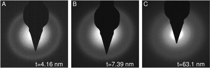
Once it became clear that the short range order does indeed depend on the thickness of the amorphous film, and having noticed that some of these amorphous films crystallized after being exposed for some time (about 15 minutes) to the electron beam in the TEM, we wanted to further investigate how the short range order evolves, while still in the amorphous state, during exposure to the electron beam and just before the amorphous to crystalline transformation. To this end, time-dependent EELS measurements were performed on amorphous alumina films of varying thicknesses (Fig. 4). A constant area of each sample was exposed to a focused electron beam (with the same parameters between different samples) and EELS measurements on Al L2,3-edge were performed with one minute intervals between them. The calibration was the same for all samples.
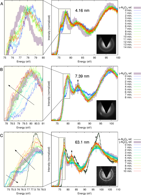
For the thinnest sample (4.16 nm), Fig. 4A clearly shows that fast rising and some smoothing of the initially extremely prominent shoulder feature occurred, but afterwards, this feature continued oscillating around the same point, and overall, there were hardly any changes in other features of the spectrum. Even after 20 minutes of exposure and measurements, the short range order did not stabilize on a specific state, but kept fluctuating back and forth. After the time-resolved measurement we switched to diffraction mode, and found that the sample remained in its amorphous state, and did not crystallize (see insert in Fig. 4A).
In another film, which was just 3 nm thicker (7.39 nm; Fig. 4B), the behavior was different: smoothing of the shoulder feature was continuous, and simultaneously, another peak started appearing and increasing in intensity at approximately 84.7 eV. Interestingly, it can be seen that the spectrum continuously moves towards resembling that of the -\ceAl2O3, until at some point it overlaps it perfectly. Here we want to stress the remarkable finding that the short range order evolved continuously towards that of the -\ceAl2O3, even before crystallization took place. At the end of this measurement, we again switched to diffraction mode, which took several minutes while the beam was still focused on the same area, and noticed a very strange pattern (see insert in Fig. 4B). No diffraction rings could be seen, however at one azimuthal angle a clustered scatter of points appeared. This is very surprising, as it implies that the sample crystallized under the beam at a highly preferred orientation. Even more surprising is the fact that this pattern has a wide range of d-spacings. At this point we cannot fully explain this phenomenon, but we can state that at some point we probably did, locally, crystallize the film.
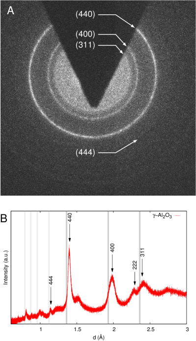
Finally, we similarly investigated a considerably thicker sample (63.1 nm). In this case we again noticed a time-resolved change in the short range order: the shoulder feature decreased considerably, and the spectrum exhibited some -\ceAl2O3–like features with time (Fig. 4C). It should be pointed out, however, that in this case we did not get a perfect overlap between the final spectrum and any of the reference spectra. The final spectrum was close to that of -\ceAl2O3, despite the appearance of few -\ceAl2O3–like features. In this case, switching to diffraction mode clearly revealed polycrystalline diffraction rings attributable to -\ceAl2O3 (fig. S3), but there was no sign of crystalline -\ceAl2O3.
These results clearly show that the short range order in an amorphous material does change as a function of thickness (size). This is of great importance, among other reasons because the short range order in an amorphous material influences the crystalline structure succeeding after it’s crystallization. The EELS analysis coincides with the XPS data, which show that the surface of amorphous alumina possesses a different short range order than the average in it’s bulk, and the thinner, or smaller, the amorphous solid is, the more it’s short range order resembles that near the surface. This phenomenon is due to the stronger effect that the surface exerts on the bulk as the size decreases. The surface structure we observed in our study agrees with what was predicted by molecular dynamics simulations[27].
This study demonstrates that the short range order in amorphous materials can indeed be altered via size effects, just as the lattice parameters of crystalline materials can be altered by them. We believe that these findings will open up new areas of research, as well as drive towards the ability to control the short range order of amorphous materials, where this is a cardinal issue that could not be previously addressed, due to the lack of possibility of such control.
Acknowledgments
The research that yielded these results received funding from the European Research Council under the European Union’s Seventh Framework Program (FP/2007–2013)/ERC Grant Agreement no [336077]. We thank Dr. L. Burstein from the Wolfson Applied Materials Research Center, Tel Aviv University, for the XPS measurements, and Dr. I. Levin, Prof. W. Kaplan, Dr. O. Kreinin, and Dr. K. Jorissen for helpful discussions.
References
- [1] S. Weiner and L. Addadi, “Crystallization pathways in biomineralization,” Annual Review of Materials Research, vol. 41, no. 1, pp. 21–40, 2011.
- [2] S. Weiner, I. Sagi, and L. Addadi, “Choosing the crystallization path less traveled,” Science, vol. 309, no. 5737, pp. 1027–1028, 2005.
- [3] P. Fratzl, F. D. Fischer, J. Svoboda, and J. Aizenberg, “A kinetic model of the transformation of a micropatterned amorphous precursor into a porous single crystal,” Acta Biomaterialia, vol. 6, no. 3, pp. 1001–1005, 2010.
- [4] J. Aizenberg, L. Addadi, S. Weiner, and G. Lambert, “Stabilization of amorphous calcium carbonate by specialized macromolecules in biological and synthetic precipitates,” Advanced Materials, vol. 8, no. 3, pp. 222–226, 1996.
- [5] L. Addadi, S. Raz, and S. Weiner, “Taking advantage of disorder: Amorphous calcium carbonate and its roles in biomineralization,” Advanced Materials, vol. 15, no. 12, pp. 959–970, 2003.
- [6] L. B. Gower, “Biomimetic model systems for investigating the amorphous precursor pathway and its role in biomineralization,” Chemical reviews, vol. 108, no. 11, pp. 4551–4627, 2008.
- [7] D. A. Drabold, “Topics in the theory of amorphous materials,” The European Physical Journal B, vol. 68, no. 1, pp. 1–21, 2009.
- [8] S. R. Elliott, Physics of Amorphous Materials. Essex, UK: Longman, 2 ed., 6 1990.
- [9] E. Zolotoyabko, Basic Concepts of Crystallography. Weinheim, Germany: Wiley-VCH, 5 2011.
- [10] D. Braga, F. Grepioni, and A. G. Orpen, eds., Crystal Engineering: From Molecules and Crystals to Materials. Springer, 9 1999.
- [11] R. Berry, “Thermodynamics – size is everything,” Nature, vol. 393, pp. 212–213, MAY 21 1998.
- [12] A. Navrotsky, “Nanoscale effects on thermodynamics and phase equilibria in oxide systems,” ChemPhysChem, vol. 12, no. 12, pp. 2207–2215, 2011.
- [13] C. Mays, J. Vermaak, and D. Kuhlmann-Wilsdorf, “On surface stress and surface tension: Ii. determination of the surface stress of gold,” Surface Science, vol. 12, no. 2, pp. 134–140, 1968.
- [14] C. Solliard and M. Flueli, “Surface stress and size effect on the lattice parameter in small particles of gold and platinum,” Surface Science, vol. 156, Part 1, no. 0, pp. 487–494, 1985.
- [15] J. M. McHale, A. Auroux, A. J. Perrotta, and A. Navrotsky, “Surface energies and thermodynamic phase stability in nanocrystalline aluminas,” Science, vol. 277, no. 5327, pp. 788–791, 1997.
- [16] R. C. Garvie, “Stabilization of the tetragonal structure in zirconia microcrystals,” The Journal of Physical Chemistry, vol. 82, no. 2, pp. 218–224, 1978.
- [17] F. Fischer, T. Waitz, D. Vollath, and N. Simha, “On the role of surface energy and surface stress in phase-transforming nanoparticles,” Progress in Materials Science, vol. 53, no. 3, pp. 481–527, 2008.
- [18] S. M. George, “Atomic layer deposition: An overview,” Chemical Reviews, vol. 110, no. 1, pp. 111–131, 2010. PMID: 19947596.
- [19] I. Levin and D. Brandon, “Metastable alumina polymorphs: Crystal structures and transition sequences,” Journal of the American Ceramic Society, vol. 81, no. 8, pp. 1995–2012, 1998.
- [20] I. Levin, A. Berner, C. Scheu, H. Muellejans, and D. Brandon, “Electron energy-loss near-edge structure of alumina polymorphs,” in Modern Developments and Applications in Microbeam Analysis (G. Love, W. Nicholson, and A. Armigliato, eds.), vol. 15 of Mikrochimica Acta Supplement, pp. 93–96, Springer Vienna, 1998.
- [21] V. Edlmayr, T. P. Harzer, R. Hoffmann, D. Kiener, C. Scheu, and C. Mitterer, “Effects of thermal annealing on the microstructure of sputtered al2o3 coatings,” Journal of Vacuum Science & Technology A: Vacuum, Surfaces, and Films, vol. 29, no. 4, pp. 041506–041506–8, 2011.
- [22] R. Brydson, “Multiple scattering theory applied to elnes of interfaces,” Journal of Physics D: Applied Physics, vol. 29, no. 7, p. 1699, 1996.
- [23] A. R. González-Elipe, J. P. Espinós, G. Munuera, J. Sanz, and J. M. Serratosa, “Bonding-state characterization of constituent elements in phyllosilicate minerals by xps and nmr,” The Journal of Physical Chemistry, vol. 92, no. 12, pp. 3471–3476, 1988.
- [24] T. Ebina, T. Iwasaki, A. Chatterjee, M. Katagiri, and G. D. Stucky, “Comparative study of xps and dft with reference to the distributions of al in tetrahedral and octahedral sheets of phyllosilicates,” The Journal of Physical Chemistry B, vol. 101, no. 7, pp. 1125–1129, 1997.
- [25] C. S. Fadley, “Angle-resolved x-ray photoelectron spectroscopy,” Progress in Surface Science, vol. 16, no. 3, pp. 275–388, 1984.
- [26] C. J. Powell and A. Jablonski, NIST Electron Effective-Attenuation-Length Database. Gaithersburg, MD: National Institute of Standards and Technology, 2011. Version 1.3.
- [27] S. P. Adiga, P. Zapol, and L. A. Curtiss, “Atomistic simulations of amorphous alumina surfaces,” Phys. Rev. B, vol. 74, p. 064204, Aug 2006.
Supplementary Materials
S1. Materials and Methods
Atomic Layer Deposition (ALD):
The ALD device used for these experiments was R-200 (Picosun, Finland). The growth process of \ceAl2O3 films utilized trimethylaluminum (TMA) and \ceH2O as precursors for deposition on Si wafers and TEM grids. The thickness of the films was determined by ellipsometry, directly on the Si wafer sample or, for other substrates, on a piece of Si wafer that was placed close to the sample during the growth process for this purpose.
Scanning Electron Microscopy (SEM):
The image in Fig. 1 was obtained with the Zeiss Ultra Plus High Resolution FEG-SEM (Zeiss, Germany), operated at 4.0 kV, using an in-lens secondary electrons (SE) detector.
Electron Energy Loss Spectroscopy (EELS):
An FEI Titan 80–300 S/TEM (FEI, Eindhoven, The Netherlands) was operated at 300 KeV and was equipped with an image Cs corrector. A post-column energy filter (Tridiem 866 ERS, Gatan, USA) was used to obtain the EELS measurements. The measured energy spread of the beam was 0.6 eV, and a dispersion of 0.03 eV/channel was used.
In order to avoid the influence of sample exchange on the spectra, several coated grids were cut and placed on a single sample holder for the comparative measurements.
X-ray Photoelectron Spectroscopy (XPS):
XPS measurements were performed in UHV ( Torr base pressure) using the 5600 Multi-Technique System (PHI, USA). Samples were irradiated with an Al Kα monochromated source (1486.6 eV) and the outcome electrons were analyzed by a spherical capacitor analyzer using a slit aperture of 0.8 mm. Sample charging during measurements was compensated by means of a neutralizer, with additional mathematical shift used when necessary (C1s at 285 eV was taken as an energy reference for all the measured peaks). The high resolution measurements presented in figure 3 were taken in a low energy range window with pass energy (PE) of 11.75 eV and 0.05 eV/step.
S2. Figures