Second harmonic generation in GaAs photonic crystal cavities in (111)B and (001) crystal orientations
Abstract
We demonstrate second harmonic generation in photonic crystal cavities in (001) and (111)B oriented GaAs. The fundamental resonance is at 1800 nm, leading to second harmonic below the GaAs bandgap. Below-bandgap operation minimizes absorption of the second harmonic and two photon absorption of the pump. Photonic crystal cavities were fabricated in both orientations at various in-plane rotations of the GaAs substrate. The rotation dependence and farfield patterns of the second harmonic match simulation. We observe similar maximum efficiencies of 1.2 %/W in (001) and (111)B oriented GaAs.
keywords:
nanophotonics, semiconductor microcavities, photonic crystals, nonlinear optics+16507230115 \alsoaffiliationDepartment of Materials Science and Engineering, Stanford University, Stanford CA 94305 \alsoaffiliationDepartment of Materials Science and Engineering, Stanford University, Stanford CA 94305 \alsoaffiliationPaul-Drude-Institut für Festkörperelektronik, Hausvogteiplatz 5-7 D-10117, Berlin, Germany
Photonic crystal cavities are excellent candidates for nonlinear optical devices, due to their low mode-volume and high quality (Q) factor. As discussed previously 1, 2, in such optical cavities, the optical mode volume is small compared to the material nonlinear coherence length, and the phase matching condition is replaced by the requirement of large mode overlap between the relevant optical modes. This offers an additional advantage for III-V semiconductor materials, which possess high nonlinearity but no birefringence. Many different approaches have been taken in order to overcome this limitation and take advantage of III-V materials, including growth of multiple quantum wells to induce birefringence 3, orientation patterning for quasiphasematching 4, inversion phase-matching in microdisks 5, form birefringence in waveguides 6, surface emitting cavities 7 and integration with optical microcavities 8. Integration of III-V materials with photonic crystal cavities requires only standard semiconductor processing 9, while the geometry of these cavities also allows easy integration of active gain media such as quantum dots or quantum wells 10, 11, 12, as well as potential on-chip integration with detectors, switches and modulators.
Experimentally, there have been many recent demonstrations of high efficiency, low power nonlinear processes in resonant microcavities, in particular second harmonic generation in microdisks 5, 13 and microrings 14, 15 in materials such as GaAs, GaN and AlN, as well as second harmonic generation and sum frequency generation in photonic crystal cavities in materials such as InP 16, GaP 17, GaAs 10, 12, 8 and LiNbO3 18. Millimeter sized lithium niobate microdisks have also been used for high efficiency second harmonic generation and ultra-low threshold optical parametric oscillators (OPOs) 19, 20, 21.
In order to achieve efficient nonlinear frequency conversion, it is necessary to choose a material with a nonlinear susceptibility tensor symmetry that matches the symmetry of the cavity modes well 7, 8 (e.g. by choosing crystal orientation). For photonic crystal cavities, modes can be described as having either TE-like or TM-like polarization 22. In the (001) orientation, the only allowed polarization conversion is from TE-like to TM-like modes (or from TM-like to TE-like). Moving to a different crystal orientation, such as the (111) orientation, is equivalent to rotating the electronic crystal axes relative to the photonic crystal axes, and therefore conversion from TE-like to TE-like and TM-like to TM-like modes are also allowed. Additionally, it is important to choose a transparency window that overlaps well with the experimental frequencies. GaAs has a transparency window from around 900 nm to 16 m, and so is particularly useful for nonlinear frequency conversion if all three wavelengths are within this range. Within this frequency range, GaAs is preferable to wider bandgap semiconductors such as GaP, as it has a stronger nonlinearity 23, is easier to grow in the (111) crystal orientation, and is compatible with bright gain media such as InGaAs quantum wells, and efficient quantum emitters, such as InAs quantum dots 10, 12, 24.
Here, we fabricate perturbed three hole defect (L3) photonic crystal cavities in (001) and (111)B oriented GaAs. The fundamental mode is at around 1800 nm, and thus the generated second harmonic is below the bandgap of the GaAs, leading to minimal absorption 25 and two photon absorption, which was present in the previous studies in this material 8, 12 due to their operation above the bandgap. The lack of absorption and other non-linear absorption effects allows us to more easily simulate the second harmonic mode, and to compare the simulations quantitatively with the experimentally measured far-field momentum space (k-space) of the second harmonic emission. While k-space measurements were performed in previous studies 16, 17 in other materials, here we expand upon the measurement and simulations of the generated modes, matching the simulated and experimental results, and demonstrate that the modes vary significantly with the photonic crystal cavity parameters and effective nonlinear susceptibility tensor symmetry (i.e. GaAs crystal orientation). Therefore, the semiconductor crystal orientation can be employed in addition to optical cavity design to improve the efficiency of frequency conversion 8.
Linear and nonlinear characterization of structures
Perturbed L3 photonic crystal cavities, as described in refs. 26 and 27, were fabricated in 165 nm thick (001) and (111)B = () oriented GaAs membranes grown on an AlGaAs sacrificial layer (0.878 m thick in the (001) sample, 0.8 m thick in the (111)B sample) on n-type doped substrates. The cavities were fabricated using e-beam lithography and dry etching to define the pattern, followed by HF wet etching to remove the sacrificial layer as described previously 9. The fabricated structures had lattice constant = 560-620 nm (resonant wavelengths between 1730 nm and 1900 nm) and designed hole radius = 0.3, with perturbed hole radius = 0.33. We choose these parameters in order to obtain structures with the second harmonic below the bandgap of GaAs, but detectable on a Si CCD. Fabricated photonic crystal cavities were all characterized experimentally at the fundamental (1st harmonic) wavelength with a broadband LED light source using a cross polarized reflectivity method 28, with Q factors of 3000 to 4000 measured, with a simulated mode volume of V = 0.76 .
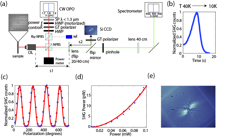
The setup for characterizing generated second harmonic is shown in Fig. 1 (a), with the flip mirror down and the 40 cm lens in place for a confocal measurement. Light from a continuous wave optical parametric oscillator (OPO) was tuned to the resonant wavelength (measured previously via cross-polarized reflectivity) of a particular cavity, and was reflected from a beam splitter and coupled to the cavity at normal incidence through a high numerical aperture (NA) objective lens. The laser power was monitored in real-time via the transmission port of the beam splitter, and the system was calibrated to calculate the power transmitted through the objective. The laser power incident on the structure was controlled with a half wave plate (HWP) on a motorized rotation stage, followed by a Glan-Thompson polarizer. The input polarization on the cavity was then controlled by a second HWP after the polarizer. The second harmonic was collected through the same objective lens, and transmitted through the beam splitter, where it was collected on a CCD spectrometer. The losses through the objective lens, beam splitter and other optics were measured and the spectrometer calibrated at the wavelength of the second harmonic to obtain the second harmonic power emitted into the numerical aperture of the objective lens. To verify the SHG is a cavity effect, rather than a bulk GaAs effect, we scanned the resonant wavelength of the cavity across the laser wavelength by scanning the temperature of the sample. While the OPO could be set to the wavelength of our choice, the tuning was not smooth and therefore to obtain a scan over the resonance it was more convenient to vary the resonant wavelength with temperature then to scan the laser. For this measurement, the sample was mounted in a liquid helium cryostat and a Zeiss objective with NA of 0.75 was used to couple light to the structure. The set temperature of the cryostat was reduced from 40 K to 10 K (this range was found to be sufficient to scan across the resonance while the cryostat remained most stable in this range). As the temperature dropped slowly, the second harmonic power was measured at equal time intervals. A resulting peak is shown in Fig. 1 (b). We only measured the actual temperature at the start and end points, while the rate of change of temperature versus time as well as the change in resonant wavelength versus temperature would be necessary in order to perform an accurate fit; our previous experiments 17 show that the Q factor follows a Lorentzian squared with the same Q factor measured in the reflectivity measurement, which in this case was 4000. However, the measurement indicates that the second harmonic process is sensitive to the resonant wavelength of the cavity.
For subsequent measurements no cryostat was present and an Olympus objective lens with NA 0.95 was used. The OPO was set to the measured wavelength of the cavity. The polarization incident on the cavity was also scanned by varying the HWP angle, as shown in Fig. 1 (c). The SHG intensity follows a dependence on HWP angle as shown by the red line fit, as expected from the L3 cavity, which is strongly polarized in the y-direction (perpendicular to the line defined by the three hole defect of the cavity). There is a phase offset as the x axis of the cavity was not aligned to 0∘ for the polarizer. The second harmonic power dependence on input power can be recorded by varying the laser power at a particular wavelength with the HWP/polarizer combination; the resulting curve for a typical cavity is shown in part (d), with a quadratic fit in red.
Farfield measurements
To obtain information about the second harmonic modes, we imaged the k-space of the second harmonic signal in (001) and (111)B oriented wafers for in-plane cavity rotations of 0∘, 30∘, 45∘, 60∘, 75∘ and 90∘ relative to the [110] or [] direction (information about which was which was not available) of the (001) oriented wafer and the [] direction of the (111) oriented wafer. The setup was in 2-2 configuration as shown in Fig. 1 (a) with the flip mirror up and the 20 cm lens in place such that = = 2 = 40 cm. The position of the camera was optimized such that a sharp image of the back aperture of the objective lens was generated. By flipping up the 40 cm lens, we could also image the real space signal on the camera as shown in Fig. 1 (e).
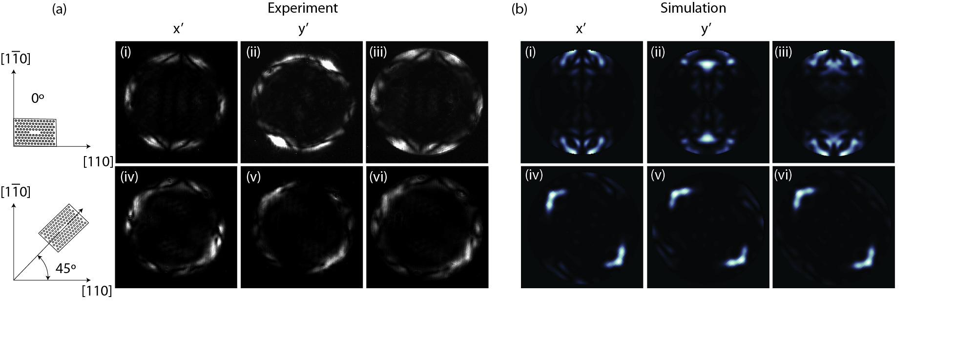
The measured farfields for lattice constant 560 nm (mean pump wavelength nm, standard deviation 6.5 nm) and 580 nm (mean nm, standard deviation 6.2 nm) in (001) oriented GaAs are shown in Fig. 2 parts (a) and (b), with rotations from 0∘ to 90∘ shown. Differences in intensity are unrelated to the actual efficiency of the device; input power was adjusted to keep the images below saturation of the camera, in order to help with identification of the modes (see Supporting Information). The k-space images for 0∘ and 45∘ in-plane rotations have very different spatial patterns, which we expect since the overlap of the fundamental and second harmonic mode changes with the rotation of the photonic crystal axes relative to the crystal axes. However, this effect is complicated by slight changes in other parameters. These additional changes for different rotations are due to differences in fabrication at different angles relative to the crystal axes and relative to the e-beam stage, which may cause variations in hole shape with in-plane rotation angle. We observe that the resonant wavelength within a particular rotation in the (001) orientation varies by 3 nm, while the mean resonant wavelength decreases by 17 nm between 0 and 75∘ rotations (with a slight increase again for 90∘). Simulations indicate that the membrane thickness and wavelength have a large effect on the mode observed (see simulations section). This is consistent with what we observe, as even the 3.5 % change in lattice constant from 560 nm to 580 nm with corresponding shift in resonant wavelength from 1760 nm to 1800 nm has a noticeable effect on the farfield, as can be seen in the difference between Fig. 2 (a) and (b). Additionally, at these wavelengths there is rapidly increasing absorption as the second harmonic approaches the bandgap 25, which could also affect the mode, in particular for the 560 nm lattice constant.
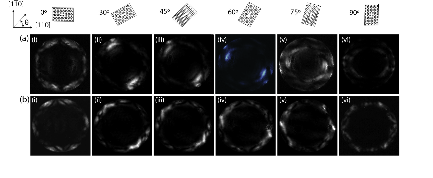
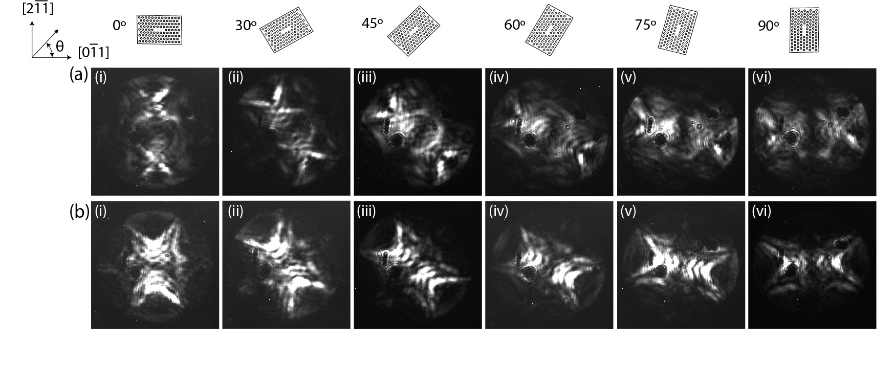
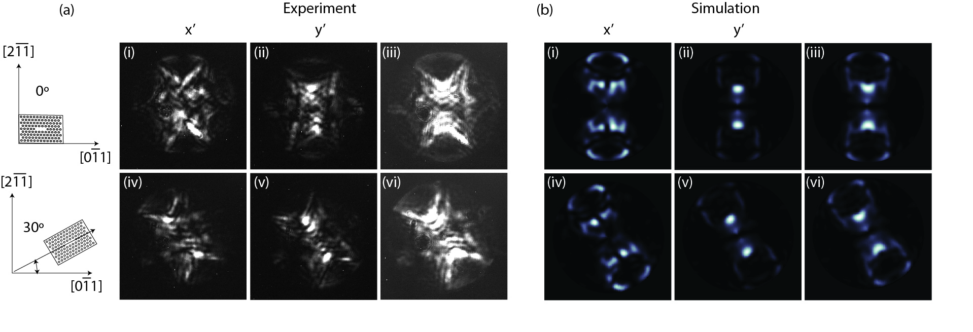
Fig. 3 shows the same measurement for the (111)B orientation, with (a) = 600 nm (mean nm, standard deviation = 3 nm) and (b) = 620 nm (mean nm, standard deviation = 3.8 nm). Despite the fact that the membranes were nominally the same thickness, in order to maintain the same resonant wavelength as in the (001) orientation it was necessary to increase the lattice constant by 40 nm, which indicates either a thinner membrane, larger etched hole radius or larger refractive index; the exact cause was difficult to determine via SEM images of the structures. In this case, there is again a decrease in average resonant wavelengths across rotations from 0 to 75∘, but in this case of only 7.5 nm, while the maximum variation within a rotation is larger (6 nm, although on average it is lower than this). The larger intra-rotation variation in the (111)B orientation is likely due to a higher number of surface defects in this wafer.
The mode k-space distribution observed is very different for the two orientations, and also changes less with rotation of the L3 in the plane of the wafer in the (111)B-orientation, which matches our simulations (see simulations section).
Second harmonic conversion efficiency
As second harmonic generation is a quadratic process at low powers, the conversion efficiency per Watt () remains constant (see Supporting Information). By measuring the second harmonic power versus input power for a particular structure, we obtain a plot as shown in Fig. 1 (d). Fitting this plot, we obtain a constant value for . We measured 12 cavities (including different in-plane rotations) in each wafer orientation, = 580 nm in the (001) oriented wafer, = 620 nm in the (111)B oriented wafer, as discussed in the farfields section. The maximum measured conversion efficiency per Watt for both (001) and (111)B oriented GaAs was 1.2 %/W, although there was again a large structure to structure variation even at a particular in-plane rotation, perhaps due to the strong sensitivity to in- and out-coupling (see Supporting Information), which will vary due to small variations in structures as well as alignment. By comparison, previous studies in similar structures in GaP 17 reported a similar total conversion efficiency per Watt of around 0.9 %/W at telecommunications wavelengths, and a much reduced efficiency per Watt of 0.002%/W in GaAs at telecommunications wavelengths 8. We discuss how this compares to simulations in the simulations section.
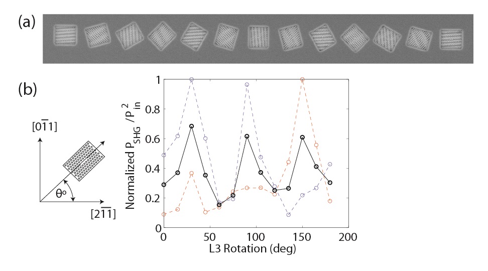
Due to the symmetry of the nonlinear susceptibility tensor, the efficiency of the second harmonic process will vary with in-plane rotation of the photonic crystal cavity (see Supporting Information). To verify the rotation dependence for structures in the (111)B orientation, we fabricated a second chip with more cavities with in-plane rotations relative to the direction. Rotations were every 15∘ from 0∘ to 180∘, as shown in the SEM in Fig. 4 (a) and lattice constant was 620 nm. The cavities had mean fundamental resonant wavelength 1803.3 nm, with a standard deviation of 1.7 nm. The stripes visible in the SEM are an artifact of the SEM. We plot normalized efficiency per unit power versus rotation for two rows of structures with the same parameters, shown in red and blue in Fig. 4 (b). The plots were normalized to the maximum value for each row, and the mean of the two is plotted in black, where we see a periodicity as a function of in-plane rotation. This is expected due to to the fact that a rotation in the (111) orientation is equivalent to an inversion of the crystal axes, combined with the symmetry of the photonic crystal cavity (see Supporting Information). Refs. 16 and 17 have previously reported variation in second harmonic signal in (001) oriented III-V semiconductors depending on the in-plane rotation of the structure.
Simulations
We next perform simulations in order to try to reproduce the farfield k-space observed in experiment and the efficiency of the second harmonic process. This is done by first simulating the fundamental mode, and then using this to generate a spatial polarization with which we can simulate the second harmonic mode. From these simulations we can estimate the in and out-coupling efficiencies we should obtain using an objective lens with numerical aperture of 0.95. Once we have the spatial profiles, coupling efficiencies and Q factors of both modes, we can estimate the low power efficiency of the device. We additionally explore the parameter space around our device in order to determine the sensitivity of the device to design parameters, and to explore the possibility to engineer higher efficiency devices.
The fundamental mode was simulated by finite difference time domain simulations (FDTD). As discussed in the farfields section, despite the fact that we use nominally the same membrane thickness, to maintain the same resonant wavelength we need to increase the lattice constant by 40 nm in (111)B GaAs compared to (001) GaAs. In order to precisely match the fundamental mode wavelengths to the simulation, the radius of the hole radii and thickness of the membrane were adjusted around the designed values. Simulations of the fundamental mode indicate that for a membrane thickness of 165 nm, a radius of 0.28 is consistent with the measured resonant frequencies for (001) oriented GaAs structures, while a radius of 0.3 is consistent with the (111)B oriented GaAs resonant frequencies. The relative size of perturbed holes was maintained constant. However, we found better agreement with second harmonic simulations by varying the membrane thickness.
The radiative () and total () Q factors of the photonic crystal cavities were calculated from simulations, in order to obtain an estimate for the cavity coupling efficiency. We take the coupling efficiency , where is the fraction of the radiated light (coupled to the cavity from vertically above it) through the NA of the objective lens. This fraction is calculated from the fraction of the radiation vectors within the light cone that also have k-vectors within the NA of the lens. We simulate the farfield by performing the fourier transform the complex fields a distance above the surface of the slab as described in references29 and 30.
In order to simulate the second harmonic mode, we generate a polarization from the fundamental mode, which is the initial excitation for our simulation:
| (1) |
where is 1 wherever there is semiconductor, and 0 in air. This generated polarization will be different in the case of the (001) and (111) orientations and will also depend on the rotation of the L3 cavity with respect to the crystal axes in the plane of the wafer (see Supporting Information). We calculate the farfield for the simulated modes to compare these to experiment. These modes were particularly sensitive to the membrane thickness of the structure. Therefore we varied the membrane thickness of the cavity around the experimental values while maintaining the correct fundamental wavelength. For each simulation, we calculated the overlap of simulated and experimental k-space in order to find the best match (see Supporting Information).
Implicit so far has been the assumption that the nonlinearity is due to bulk effects, while the nanocavity employed has is a significant surface to volume ratio. The symmetry of the surface is different than the bulk effect 31, although in the case of (001)-GaAs the (001) surface (which is the main surface seen by the mode) nonlinearity still prevents TE-TE mode coupling. Our simulations of surface versus bulk overlap indicate that while the surface may contribute slightly to the second harmonic signal, the main contribution is from the bulk nonlinearity. This is in agreement to the conclusions found in previous studies of photonic crystal cavities 32. Experimentally, by performing measurements on a number of structures rotated in-plane , it should be possible to distinguish the surface from bulk contributions 31. However, this effect is complicated due to the fact that the second harmonic mode is very sensitive and will change depending on the excitation, and any measurement would need to be statistical over many structures, as the polarization is set by the in-plane rotation of the cavity. As there is significant structure to structure variation due to fabrication imperfections, such an effect may be impossible to measure. Even the rotation dependence of the surface will depend significantly on the presence of any native oxides or surface contamination 33.
Figs. 5 and 6 show (a) experimental and (b) simulated k-space images for (001) and (111) orientations, with simulations plotting up to NA = 0.95. For the (001) orientation, we compare the experimentally measured and simulated k-space images for both 0 and 45 degree rotations for the cavity mode with resonant frequency at 1800 nm, while for (111) orientation we compare 0 and 30 degree rotations with simulations. The (001) oriented cavity simulation was consistent with a membrane thickness of 165 nm. The (111) orientation simulation indicated a membrane thickness of 150 nm.
For triply resonant cavity processes at low input powers, the second harmonic power is proportional to the input power as
| (2) |
(see Supporting Information) where and are the quality factors of the fundamental and second harmonic modes, and are the input/output coupling efficiencies of the fundamental and second harmonic modes and is a non-linear overlap integral given by 2, 34,
| (3) |
whose value for a particular set of modes depends on the magnitude and symmetry of . From equation 2 we can see that the conversion efficiency is very sensitive to the Q factors of both modes, as well as to the coupling efficiency.
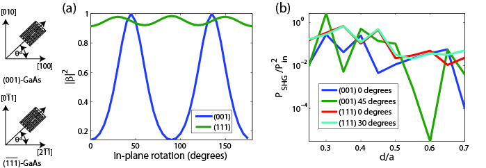
Using these simulations, we can make estimates of this nonlinear overlap integral, as well as of the total Q and coupling Q factors of the second harmonic mode. We verify that the simulations give us the expected in-plane rotation dependence in Fig. 7 (a), where we plot the nonlinear overlap (each normalized to its maximum value) versus the in-plane rotation for (001) and (111) orientations, and obtained the expected 60 degree and 90 degree symmetries. From equation 3, we can calculate the simulated efficiency per Watt input power.
The fundamental and second harmonic modes were simulated for increasing (in experiment corresponding to an increase in membrane thickness, with resonant wavelength maintained constant). The plot of , shown in Fig. 7 (b), shows that the geometry of the second harmonic mode is very important in calculating the overall efficiencies. From this plot, we estimate efficiencies of the order of 10 %/W for both (001) and (111) orientations, compared to the experimentally measured values of the order of 1%/W. The internal conversion efficiency can also be estimated using the simulated coupling efficiency values (around 30) to give a simulated internal efficiency of 370/W. These calculated coupling efficiencies are likely higher than the experimentally achieved coupling efficiency, and could explain the discrepancy between simulated and measured values.
From this plot, we see that the particular second harmonic mode excited is very important in determining the efficiency of the device. For example, depending on the particular second harmonic mode, either the 0 or 45∘ in-plane rotation in the (001) orientation can have higher efficiency. The (111) and (001) orientations also vary in relative efficiencies depending on parameters, and therefore with knowledge of the second harmonic mode we can use the wafer orientation in order to engineer higher efficiency devices. Having good control over these modes would also allow us to use microcavities in order to measure nonlinear properties of new materials, without needing to develop phase-matching and quasi-phasematching techniques. However, this is challenging in these geometries as the particular mode is very sensitive to the parameters of the device.
Engineering higher efficiency devices
The experimentally achieved efficiency of second harmonic generation in photonic crystal cavities has been limited by the difficulty of engineering multiple high quality factor modes with a high degree of overlap 16, 17, 18. This difficulty arises because the bandgap of photonic crystals does not span a sufficiently large frequency range for processes, and there are no significant higher order bandgaps. This means that only one of the modes of the photonic crystal cavity in the process is well defined and has high Q. As discussed in this work and others 16, 17, 11, 18, the second harmonic couples to leaky air band modes perturbed by the presence of the cavity which have low Q factors, low overlap with the fundamental mode, and are difficult to couple to for processes such as difference frequency conversion and optical parameteric oscillation. The SHG process goes as the square of the fundamental, so as shown in Eq. 2 it is important that the fundamental mode have a large Q. However, since we are coupling at normal incidence, increasing the Q factor will in general lead to a decrease in the coupling efficiency, and therefore increasing the Q significantly beyond a few thousand does not lead to further improvement. Creating a well defined coupling channel, such as a waveguide coupled to the photonic crystal cavity, would allow us to obtain increased benefit from higher Q. For the current structure, a better understanding of these modes outside the bandgap in photonic crystals may help to engineer higher efficiency frequency conversion. The additional degree of freedom of choosing the symmetry of the effective is also beneficial in the design of resonators. Where individual resonators with high overlap and Q factors may not be sufficient, the ability to engineer doubly resonant microcavities opens up the possibility for generating highly nonlinear materials that phasematch via engineered dispersion 35 or quasi-phasematch 36 using coupled resonator arrays. There have been several proposals for designing photonic crystal cavities with multiple high Q resonances and large frequency separations 37, 34, 38, 39, 40, 41; such a cavity could improve the efficiency of the process by several orders of magnitude.
Integration of nonlinear microcavities with quantum dots for quantum optics and quantum information processing is also of current interest. Cavities such as those used in this work could be useful for high signal to noise resonant excitation of InAs QDs 10. Additionally, frequency conversion of flying qubits to telecommunications wavelength or to optimal detection wavelengths is desirable 42, and has been demonstrated using off-chip periodically poled lithium niobate waveguides. Self-frequency conversion of high density quantum dots in a photonic crystal cavity has been recently demonstrated, 12, 24, but demonstrations of frequency conversion of single quantum dots coupled to on-chip microcavities has yet to be demonstrated. In particular, frequency conversion between InAs QD wavelengths and telecommunications wavelength requires intra-cavity difference frequency generation, which is again challenging, due to the long wavelength of the pump, and difficulties in engineering photonic crystal cavities with well defined and overlapping modes at sufficiently large wavelength separations. This work demonstrates the characterization and operation of these cavities in GaAs at longer wavelengths than previously demonstrated.
Conclusion
We demonstrate second harmonic generation below the bandgap in photonic crystal cavities in (001) and (111)B oriented GaAs. We fabricate photonic crystal structures in both (111)B and (001) oriented GaAs at different orientations with respect to the crystal axes of the GaAs substrate, and match the rotation dependence and farfield patterns to simulation. We discuss how these results are relevant to engineering higher efficiency on-chip nonlinear frequency conversion in photonic crystal cavities.
Acknowledgements
Financial support was provided by the Air Force Office of Scientific Research, MURI Center for multi-functional light–matter interfaces based on atoms and solids, National Science Graduate Fellowships, and Stanford Graduate Fellowships. This work was performed in part at the Stanford Nanofabrication Facility of NNIN supported by the National Science Foundation under Grant No. ECS-9731293, and at the Stanford Nano Center. J.V. also thanks the Alexander von Humboldt Foundation for support. K.G.L. acknowledges support from the Swiss National Science Foundation.
Appendix
Appendix A Photonic crystal polarization and semiconductor orientation
The vertical symmetry of the photonic crystal cavity forces all modes to be either primarily transverse electric (TE)-like or transverse magnetic (TM)-like 22. For a TE-like mode, , , and obey even symmetry in the vertical direction about the center of the slab while at the central plane and are anti-symmetric about this plane (where we define as the direction normal to the wafer, and and to be in the plane of the wafer). For TM-like modes, , , and obey even symmetry in the vertical direction about the center of the slab while at the central plane and are anti-symmetric about this plane.
For (100) oriented III-V semiconductors, the second order nonlinear susceptibility tensor is given by
| (4) |
where the generated polarization at a sum frequency can be calculated by
| (5) |
For GaAs the matrix found in the literature is defined such that are the (100), (010) and (001) axes of the crystal structure (while the cleave axes in GaAs are the (110) and equivalent planes). This means that for the case of (001) GaAs the and coordinates are in the same plane as two of the major crystal axes, and can be chosen to be aligned with the crystal axes. Examining the mode overlap integral reveals that for the process of second harmonic generation, a TE-like mode may only couple to a TM-like mode if the wafer is normal to the [100], [010], or [001] (equivalent) directions, as in standard (001) oriented wafers.
In the case of (111) GaAs, the plane of the wafer is no longer the same as the plane of crystal axes. The values of E-field can be either transformed to this coordinate system or a new matrix can be derived with , in the plane of the wafer. Rotating from the (001) to the (111) plane can be done by applying the following steps: (1) rotation about the z-axis of 45 degrees (2) rotation through an angle of about the y-axis.
This gives the matrix
| (6) |
The calculated is given by
| (7) |
We can see that this new matrix leads to coupling between TE-like polarizations, e.g. . The tensor leads to the expected 120 degree symmetry, with the effective and axes along the [11] and [10] directions.
Appendix B Calculation of low power efficiency
Following refs. 2 and 46, the coupled mode equations for a nonlinearity with two modes, one at fundamental frequency and the second at the second harmonic frequency , are
| (8) |
| (9) |
where is the time independent complex amplitude of the the mode, with normalized to electromagnetic energy stored in the mode. is the nonlinear coupling between the two modes, and is given by the nonlinear overlap integral in Eq. 3 in the text 2, 46. is the amplitude of the incoming () or outgoing () wave, and in this case .
| (10) |
In steady state, the second harmonic output power in terms of
| (11) |
and the input power in terms of
| (12) |
Therefore, at low input powers, when we have that
| (13) |
and therefore vs. is quadratic at low powers, with efficiency per unit input power a constant given by
| (14) |
Appendix C Simulation inputs
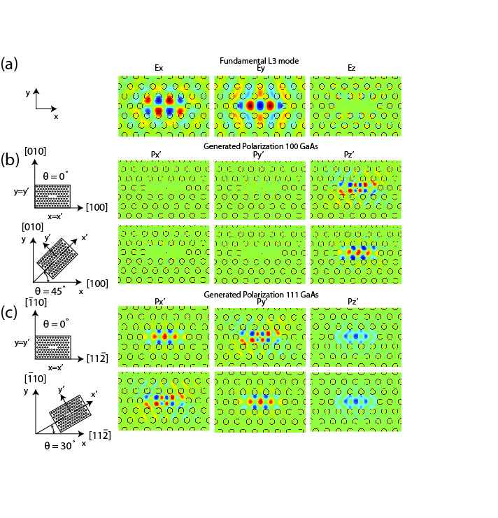
Fig. 8 shows the generated polarizations at the center of the photonic crystal membrane for the (001) orientation for 0∘ and 45∘ in plane rotations and in the (111) orientation for 0∘ and 30∘ in-plane rotations. We generate this field profile for the full 3D space of the simulation using a current sources, and allow the field to evolve in time. The refractive index is changed in this simulation to match the refractive index at the second harmonic wavelength 25.
Appendix D Far field simulation and experimental image comparison
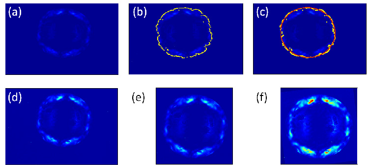
To obtain theoretical understanding of the SHG process in the cavities, we analyze far field image of the second harmonic mode, by comparing experimental and simulation data.
Due to alignment imperfections of beam to the camera, and the photonic crystal relative to the x-y axes, and deflection of the beam by the polarizer, the experimental images are skewed and rotated (Fig. 9 (a)) compared to the coordinate system used in the simulation. To facilitate a successful image comparison, we first develop a data-specific algorithm to resize and rotate the experimental image. The data-specific content in this case is the k-space of the second harmonic emission, the outer edge of which is defined by the edge of the image of the back aperture of the objective lens. Outside of this aperture there is negligible intensity. Due to imperfect alignment, the image of this aperture is an ellipse instead of a circle, which varies from image to image due to alignment adjustments that were made over the course of the experiment. We identify this shape by finding the edge contour of the signal region, where the signal value jumps (Fig. 9 (b)). Then, we fit that contour to an ellipse (Fig. 9 (c)), and use the fit parameters (ratio between long and short ellipse axes) to rescale the image and obtain a circular signal (Fig. 9 (d)). We use the coordinates of the center and radius of the new circle to crop the image around the relevant signal (Fig. 9 (e)). Finally, we rotate the image to match the coordinates of the simulation (Fig. 9 (f)).
Comparison between the processed experimental and simulation images was done by the following correlation algorithm
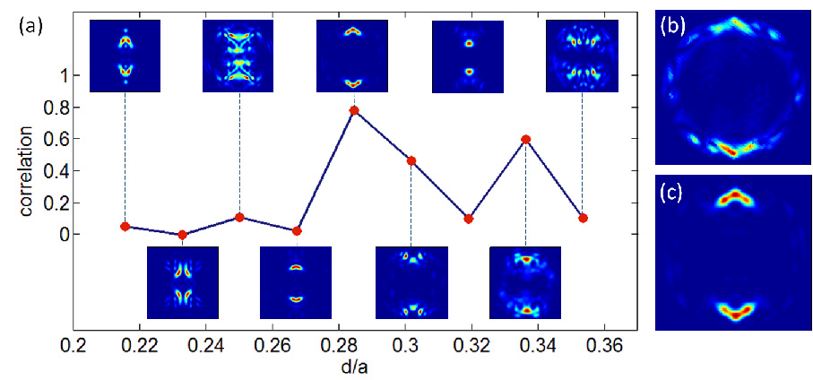
To find the best correlation between the two images, we vary zoom, rotation, and x and y translation of the experimental image, recording the maximal correlation value as a figure of merit. Fig. 10 (a) shows the dependence of the correlation value between a processed experimental image (Fig. 10) ((001) orientation, = 580 nm, in-plane rotation 45 degrees) and simulated patterns for increasing slab thicknesses with resonant wavelength maintained constant (insets in the plot), and are consistent with a simple visual inspection. Fig. 10 (c)) shows the simulation pattern with highest correlation value to the processed experimental image in Fig. 10 (b).
References
- Liscidini and Andreani 2004 Liscidini, M.; Andreani, L. C. Applied Physics Letters 2004, 85, 1883–1885
- Rodriguez et al. 2007 Rodriguez, A.; Soljačić, M.; Joannopoulos, J. D.; Johnson, S. G. Optics Express 2007, 15, 7303–7318
- Fiore et al. 1998 Fiore, A.; Berger, V.; Rosencher, E.; Bravetti, P.; Nagle, J. Nature 1998, 391, 463–466
- Eyres et al. 2001 Eyres, L. A.; Tourreau, P. J.; Pinguet, T. J.; Ebert, C. B.; Harris, J. S.; Fejer, M. M.; Becouarn, L.; Gerard, B.; Lallier, E. Applied Physics Letters 2001, 79, 904–906
- Kuo et al. 2014 Kuo, P. S.; Bravo-Abad, J.; Solomon, G. S. Nature Communications 2014, 5
- Stievater et al. 2014 Stievater, T. H.; Mahon, R.; Park, D.; Rabinovich, W. S.; Pruessner, M. W.; Khurgin, J. B.; Richardson, C. J. K. Optics Letters 2014, 39, 945–948
- Vakhshoori et al. 1991 Vakhshoori, D.; Fischer, R.; Hong, M.; Sivco, D.; Zydzik, G.; Chu, G.; Cho, A. Applied Physics Letters 1991, 59, 896
- Buckley et al. 2013 Buckley, S.; Radulaski, M.; Biermann, K.; Vučković, J. Applied Physics Letters 2013, 103, 211117
- Khankhoje et al. 2010 Khankhoje, U. K.; Kim, S.-H.; Richards, B. C.; Hendrickson, J.; Sweet, J.; Olitzky, J. D.; Khitrova, G.; Gibbs, H. M.; Scherer, A. Nanotechnology 2010, 21, 065202
- Rivoire et al. 2011 Rivoire, K.; Buckley, S.; Majumdar, A.; Kim, H.; Petroff, P.; Vučković, J. Applied Physics Letters 2011, 98, 083105–083105–3
- Buckley et al. 2012 Buckley, S.; Rivoire, K.; Hatami, F.; Vučković, J. Applied Physics Letters 2012, 101, 161116–161116–4
- Ota et al. 2013 Ota, Y.; Watanabe, K.; Iwamoto, S.; Arakawa, Y. Optics Express 2013, 21, 19778–19789
- Xiong et al. 2011 Xiong, C.; Pernice, W.; Ryu, K. K.; Schuck, C.; Fong, K. Y.; Palacios, T.; Tang, H. X. Optics Express 2011, 19, 10462–10470
- Levy et al. 2011 Levy, J. S.; Foster, M. A.; Gaeta, A. L.; Lipson, M. Optics Express 2011, 19, 11415–11421
- Pernice et al. 2012 Pernice, W. H. P.; Xiong, C.; Schuck, C.; Tang, H. X. Applied Physics Letters 2012, 100, 223501–223501–4
- McCutcheon et al. 2007 McCutcheon, M. W.; Young, J. F.; Rieger, G. W.; Dalacu, D.; Frédérick, S.; Poole, P. J.; Williams, R. L. Physical Review B 2007, 76, 245104
- Rivoire et al. 2009 Rivoire, K.; Lin, Z.; Hatami, F.; Masselink, W. T.; Vučković, J. Optics Express 2009, 17, 22609–22615
- Diziain et al. 2013 Diziain, S.; Geiss, R.; Zilk, M.; Schrempel, F.; Kley, E.-B.; Tünnermann, A.; Pertsch, T. Applied Physics Letters 2013, 103, 051117–051117–4
- Ilchenko et al. 2003 Ilchenko, V. S.; Matsko, A. B.; Savchenkov, A. A.; Maleki, L. Journal of the Optical Society of America B 2003, 20, 1304–1308
- Fürst et al. 2010 Fürst, J. U.; Strekalov, D. V.; Elser, D.; Lassen, M.; Andersen, U. L.; Marquardt, C.; Leuchs, G. Physical Review Letters 2010, 104, 153901
- Förtsch et al. 2013 Förtsch, M.; Fürst, J. U.; Wittmann, C.; Strekalov, D.; Aiello, A.; Chekhova, M. V.; Silberhorn, C.; Leuchs, G.; Marquardt, C. Nature Communications 2013, 4, 1818
- Joannopoulos et al. 2011 Joannopoulos, J. D.; Johnson, S. G.; Winn, J. N.; Meade, R. D. Photonic Crystals: Molding the Flow of Light (Second Edition); Princeton University Press, 2011
- Shoji et al. 1997 Shoji, I.; Kondo, T.; Kitamoto, A.; Shirane, M.; Ito, R. Journal of the Optical Society of America B 1997, 14, 2268–2294
- Ota et al. 2013 Ota, Y.; Watanabe, K.; Iwamoto, S.; Arakawa, Y. Applied Physics Letters 2013, 103, 243115
- Palik 1985 Palik, E. D. Handbook of Optical Constants of Solids, Volumes I, II, and III: Subject Index and Contributor Index; Elsevier Science & Tech, 1985
- Toishi et al. 2009 Toishi, M.; Englund, D.; Faraon, A.; Vučković, J. Optics Express 2009, 17, 14618–14626
- Portalupi et al. 2010 Portalupi, S. L.; Galli, M.; Reardon, C.; Krauss, T.; O’Faolain, L.; Andreani, L. C.; Gerace, D. Optics Express 2010, 18, 16064–16073
- Altug and Vuckovic 2005 Altug, H.; Vuckovic, J. Optics Express 2005, 13, 8819
- Vuckovic et al. 2002 Vuckovic, J.; Loncar, M.; Mabuchi, H.; Scherer, A. Quantum Electronics, IEEE Journal of 2002, 38, 850 –856
- Taflove and Hagness 2005 Taflove, A.; Hagness, S. C. Computational electrodynamics: the finite-difference time-domain method; Artech House: Boston, 2005
- Stehlin et al. 1988 Stehlin, T.; Feller, M.; Guyot-Sionnest, P.; Shen, Y. R. Optics Letters 1988, 13, 389–391
- McCutcheon et al. 2005 McCutcheon, M. W.; Rieger, G. W.; Cheung, I. W.; Young, J. F.; Dalacu, D.; Frédérick, S.; Poole, P. J.; Aers, G. C.; Williams, R. L. Applied Physics Letters 2005, 87, 221110
- Armstrong et al. 1992 Armstrong, S. R.; Hoare, R. D.; Pemble, M. E.; Povey, I. M.; Stafford, A.; Taylor, A. G. Journal of Crystal Growth 1992, 120, 94–97
- Burgess et al. 2009 Burgess, I. B.; Zhang, Y.; McCutcheon, M. W.; Rodriguez, A. W.; Bravo-Abad, J.; Johnson, S. G.; Loncar, M. Optics Express 2009, 17, 20099–20108
- Xu et al. 2000 Xu, Y.; Lee, R. K.; Yariv, A. Journal of the Optical Society of America B 2000, 17, 387–400
- Dumeige 2011 Dumeige, Y. Physical Review A 2011, 83, 045802
- Zhang et al. 2009 Zhang, Y.; McCutcheon, M. W.; Burgess, I. B.; Lončar, M. Optics Letters 2009, 34, 2694–2696
- Thon et al. 2010 Thon, S. M.; Irvine, W. T. M.; Kleckner, D.; Bouwmeester, D. Physical Review Letters 2010, 104, 243901
- McCutcheon et al. 2009 McCutcheon, M. W.; Chang, D. E.; Zhang, Y.; Lukin, M. D.; Lončar, M. Optics Express 2009, 17, 22689–22703
- Rivoire et al. 2011 Rivoire, K.; Buckley, S.; Vučković, J. Optics Express 2011, 19, 22198–22207
- Rivoire et al. 2011 Rivoire, K.; Buckley, S.; Vučković, J. Applied Physics Letters 2011, 99, 013114–013114–3
- Buckley et al. 2012 Buckley, S.; Rivoire, K.; Vučković, J. Reports on Progress in Physics 2012, 75, 126503
- Mabuchi 2012 Mabuchi, H. Physical Review A 2012, 85, 015806
- Majumdar and Gerace 2013 Majumdar, A.; Gerace, D. Physical Review B 2013, 87, 235319
- Irvine et al. 2006 Irvine, W. T. M.; Hennessy, K.; Bouwmeester, D. Physical Review Letters 2006, 96, 057405
- Burgess et al. 2009 Burgess, I. B.; Rodriguez, A. W.; McCutcheon, M. W.; Bravo-Abad, J.; Zhang, Y.; Johnson, S. G.; Loncar, M. Optics Express 2009, 17, 9241–9251