A \vol92 \no12 \SpecialIssue \SpecialSectionVLSI Design and CAD Algorithms \authorlist\breakauthorline2 \authorentry[disyulei@gmail.com] Bei YunlabelA \authorentry[dongsq@mail.tsinghua.edu.cn] Sheqin DongmlabelA \authorentrySong ChenmlabelB \authorentrySatoshi GOTOflabelB \affiliate[labelA]The authors are with the EDA lab, Department of Computer Science and Technology, Tsinghua University, Beijing 100084, China \affiliate[labelB]The authors are with the Graduate School of Information, Production and Systems, Waseda University, Kitakyushu-shi, 808-0135 Japan 318 622
Voltage and Level-Shifter Assignment Driven Floorplanning
keywords:
Voltage-Island, Voltage Assignment, Convex Network Flow, Level Shifter Assignment, White Space RedistributionLow Power Design has become a significant requirement when the CMOS technology entered the nanometer era. Multiple-Supply Voltage (MSV) is a popular and effective method for both dynamic and static power reduction while maintaining performance. Level shifters may cause area and Interconnect Length Overhead(ILO), and should be considered at both floorplanning and post-floorplanning stages. In this paper, we propose a two phases algorithm framework, called VLSAF, to solve voltage and level shifter assignment problem. At floorplanning phase, we use a convex cost network flow algorithm to assign voltage and a minimum cost flow algorithm to handle level-shifter assignment. At post-floorplanning phase, a heuristic method is adopted to redistribute white spaces and calculate the positions and shapes of level shifters. The experimental results show VLSAF is effective.
1 Introduction
Low Power Design has become a significant requirement when the CMOS technology entered the nanometer era. On the one hand, hundreds of millions of transistors can be integrate on the same chip by using system-on-chip(SoC) design methodologies. On the other hand, the shrinking feature sizes and increasing circuit speed cause higher power consumption, which not only shorten the battery life for handheld devices but also lead to thermal and reliability problems.
Many techniques were introduced to deal with power optimization. Among the existing techniques, MSV is a popular and effective method for both dynamic and static power reduction while maintaining performance. In the MSV design, one of the most important problem is voltage assignment: timing critical modules are assigned to higher voltage while noncritical modules are assigned to lower voltage, so the power can be saved without degrading the overall circuit performance.
Level-shifter [1] has to be inserted to an interconnect when a low voltage module drives a high voltage module or a circuit may suffer from excessive short-circuit current and leakage energy. From [5] we can observe that the number of level shifters increase rapidly as modules increase and the area level-shifters consume can not be ignored. As a result, level-shifters may cause area and performance overhead, and should be considered during floorplanning and post-floorplanning stages.
There are a number of works addressing island generation and voltage assignment in floorplanning and placement. Among these works, voltage assignment is considered at various stages, including pre-floorplanning[4, 5]; during floorplanning[6, 7, 8]; and post-floorplaning / post-placement [9, 10, 11, 12].
Lee et al.[5] handle voltage assignment by dynamic programming, and level shifters are inserted as soft block according to the voltage assignment result at pre-floorplanning stage. Then power network resource are considered during floorplanning. However, there are some deficiencies in the work: first, voltage assignment is handled before floorplanning, so physical information such as the distances among modules are not able to be taken into account; secondly, the search space is large if level-shifters are considered as a module.
An approach based on ILP is used in [10] for voltage assignment at the post-floorplanning stage. Level-shifter planning and power-network resources are considered. However, their approach does not consider level-shifter’s area consumption and relies on the floorplanning result.
To make use of physical information such as the length of interconnects among modules, voltage assignment problem should be addressed during floorplanning. Ma et al.[8] transform voltage assignment problem into a convex cost network flow problem, and integrate it into floorplanning stage. However, their approach consider neither level-shifters’ area overhead nor level-shifters’ positions.
The remainder of this paper is organized as follows. Section 2 defines the voltage-island driven floorplanning problem. Section 3 presents our algorithm flow. Section 4 reports our experimental results. At last, Section 5 concludes this paper.
2 PROBLEM FORMULATION
In this paper, we use CBL[3] to represent every floorplan generated. CBL is a topological representation dissecting the chip into rectangular rooms, and each room is assigned at most one module. Besides, all the nets are two-pin nets, and multi-pin nets can be decomposed into a set of source-sink two-pin nets. The wire length of every net is calculated by half-perimeter model.
Definition 1 (Interconnect Length Overhead)
Each
level-shifter belongs to a net, we assume that a level
shifter can always be inserted in the net’s bounding box. However,
if level-shifter is outside net’s bounding box, its net’s
interconnect length would increase. The increased length is denoted
as Interconnect Length Overhead (ILO).
Definition 2 (Power Network Resource)
The power network resource of a voltage island is evaluated by the half perimeter wirelength of the minimal bounding box enclosing the island.
For every candidate floorplan, to meet the performance constraint, timing-critical modules are assigned a high voltage, and the other non-timing-critical modules are assigned a lower voltage to maximize power saving. Besides, each level-shifter is assigned to a rough position to minimize interconnect length overhead. We refer to the problem as the Voltage and Level-Shifter Assignment driven Floorplanning (VLSAF).
Problem 1
(VLSAF) We are given
| 1) | A set of m modules: . Each |
|---|---|
| module is hard block(fixed size and aspect ratio), | |
| and is given legal working voltages, and power | |
| -delay tradeoff is represented as a delay-power curve | |
| (DP–curve, as shown in Fig.3). | |
| 2) | A netlist, which can be denoted as a directed acyclic |
| graph(DAG), , where | |
| , and denotes an interconnect from | |
| to . | |
| 3) | A timing constraint |
| 4) | Level-shifter’s area, power and delay. |
After VLSAF, a chip floorplanning is generated to meet several objectives: First, minimize the area and power cost. Secondly, satisfying timing constraint. Third, insert all the level-shifters in need and minimize the wire length and the interconnect length overhead.
3 VLSAF Algorithm
3.1 Overview of VLSAF
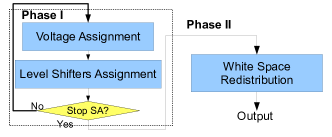
As shown in Fig.1, algorithm VLSAF consists of two phases: (I)voltage and level-shifters assignment during floorplanning, (II) White Space Redistribution(WSR) at post-floorplanning.
In Phase I, we modify the model in [8] to handle voltage assignment and present a Min-Cost Max-Flow based method to solve the level-shifters assignment problem. When generate a new packing, we carry out voltage and level-shifter assignment. After voltage assignment(VA), each module is assigned a voltage to reduce power consumption as much as possible yet satisfies the performance constraint. After level-shifter assignment(LSA), as many level-shifters as possible are assigned a room. Level shifters which can not assigned are belong to set (detail in 3.4) and will cause some Interconnect Length Overhead(ILO).
In Phase II, a heuristic method is adopted to calculate every module’s relative position in room. Besides, every room’s white space is divided into grids, and each level-shifter is decided its aspect ratio and inserted to a grid. Finally, if a level-shifter can not assign a room in LSA, it can be inserted into a room in order to reduce interconnect length overhead(ILO).
3.2 Voltage Assignment of Two Voltages
During floorplanning, when a new floorplan is generated, we can estimate the interconnect length between module i and module j, denoted as . Similar to [8], can be scaled to delay according to , where is a constant scaling factor. We check every , if , then time constraint can not be satisfied, so another new floorplan is generated. Otherwise we carry out voltage assignment.
Given netlist , voltage assignment problem can be formulated as (1):
| (1) |
where is the arrival time of vertex in DAG, and is the delay of vertex .
3.2.1 Two Legal Working Voltages Assignment
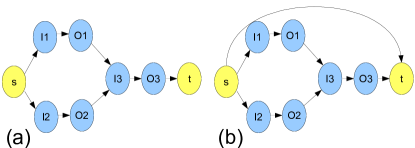
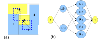
When there are only two legal working voltages, we transform into . First, a start node and an end node are added to , interconnect the nodes whose in-degree are zero, and nodes with zero out-degree interconnect . We set . Besides, are divided into two nodes: and , so . And is connected to by a directed edge. We denote these new created edges as , denote edges as , and other edges as , and . The DAG is shown in Fig. 2 (a).
Compare with [8], which has more constraints as follows:
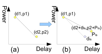
we introduce some modifications. First, timing constraint used to be estimated as , where is the longest path in DAG. To reduce tolerance of timing constraint, in module’s DP-curve, we add to lower voltage’s delay and add to lower voltage’s power(as shown in Fig. 3), and time constraint can be set as . Since there are only two possible supply voltages, power function still be convex function. Secondly, we add start node and end node to remove constraint . Third, since DP-curve is a linear function, in other word, for , has only two choices: and . We can prove later that we can solve the program optimally even if we remove the constraint .
We can incorporate constraints and by transforming into , and define , s.t. . Accordingly, , and the transformed DAG is shown in Fig.2(b). Besides, we dualize the constraints using a nonnegative Lagrangian multiplier vector , obtaining the following Lagrangian subproblem:
| (3) |
We set , remove , and add an edge for each node . The newly edges are denoted as , and , . Now , and the transformed DAG is denoted as .
For every , we set ,, where is a huge coefficient.
We define function for each as follows: .
For the , because is linear function
| (4) |
where and denotes slope of the function, .
| (7) | |||||
| (10) |
For the , .
For the ,, where if ; and if , equals .
To transform the problem into a minimum cost flow problem, we construct an expanded network . There are three kinds of edges to consider:
-
•
in E1:we introduce 2 edges in , and the costs of these edges are: ; upper capacities: ; lower capacities are both 0.
-
•
in E2: cost, lower and upper capacity is , 0, M.
-
•
Edge in E3: two edges are introduced in , one with cost, lower and upper capacity as (), another is ().
Using the cost-scaling algorithm, we can solve the minimum cost flow problem in . For the given optimal flow , we construct residual network and solve a shortest path problem to determine shortest path distance from node to every other node. By implying that and for each , we can finally solve voltage assignment problem.
3.2.2 Multi-Voltage Assignment
When number of legal working voltages is more than two, we can solve voltage assignment in a similar method.
Definition 3 (LS-DP-Curve)
The power-delay tradeoff of level shifter is represented by a LS-DP-Curve , where each pair is the corresponding delay and power consumption when level shifter is driving from module at voltage .
When a module is at voltage ( the most high voltage ), it does not need level shifter to drive other modules, . Lower voltage module needs bigger level shifter to drive other modules. Since dynamic energy consumption is proportional to the square of the supply voltage, it is trival that power increases rapidly than delay. We assume the LS-DP-Curve is convex.
For each module, we modify its DP-Curve: replace each pair by , where is level shifter’s delay and power consumption.
LEMMA 1
is convex , .
LEMMA 2
If and are convex, then is also convex.
Using lemma 1 and lemma 2, we can prove that modified DP-Curve is piecewise linear convex function with integer breakpoints, and we can apply similar method like 3.2.1 to solve voltage assignment problem.
3.3 Level Shifters Assignment
| # of modules | |
|---|---|
| # of level-shifters in need | |
| Set of rooms, | |
| Room containing module | |
| White space in | |
| Set of LSs with same source and same sink | |
| # of level shifters in | |
| Potential white space in room | |
| Width(Height) of room | |
| Width(Height) of module | |
| Width(Height) of 1st Feasible Region |
After voltage assignment, every module is assigned a voltage. Since each net driving from a low voltage module to a high voltage module should insert a level shifter, the number of level-shifters is determined. To locate the modules, chip is dissected into set of rooms . Due to the restriction that level shifter cannot be placed on a module, the location must be within a white space. Besides, level shifter has non-zero area, it cannot be placed arbitrarily close to each other.
Here we carry out minimum cost flow based level-shifters assignment to try to assign every level-shifters one room. We define sets of level shifters , every set contain level shifters with same source module and the same sink module , and .
To check whether a room has extra space to insert level-shifter, we denote the White Space in room as , whose area can be calculated as follow:
| (11) |
where denotes the width(height) of room , denotes the width(height) of module .
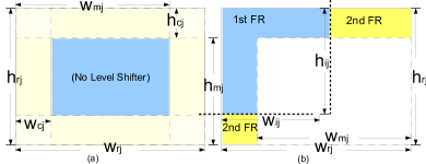
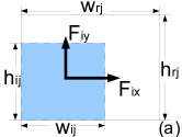
Each level-shifter belongs to a net, and is inserted into white space. If white space is outside the net’s bounding box, inserting level shifter may cause Interconnect Length Overhead(ILO), so each white space has its own cost for given level shifter. Since we assume all modules are hard blocks, some space of room must belong to a module(as shown in Fig.4(a), center dashed area can not insert level shifter no matter how to put the module).
Definition 4 (Potential White Space (PWS))
The space of room can be white space through module moving is denoted as Potential White Space().
can be considered as two horizontal channels and two vertical channels, as shown in Fig. 4 (a), we denote the width of vertical channel as , and the width of horizontal channel as .
Definition 5 (Feasible Region (FR))
For a net requiring level shifter , its bounding box is denoted as , we define level-shifter ’s feasible region as and .
For room , if its white space belongs to level-shifter ’s Feasible Region , we call as ’s candidate room. The part of in is denoted as 1st Feasible Region(), while the other part of is denoted as 2nd Feasible Region(). If is inserted into its candidate room, then will not cause Interconnect Length Overhead (ILO) to its net.
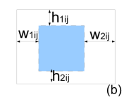
We set and , then the area of can be calculated as follows:
| (12) |
We construct a network graph , and then use a min-cost max-flow algorithm to determine which room each level shifter belong to. If all level shifters are assigned to their candidate rooms, no ILO will occur. A simple example is shown in Fig.5.
-
•
.
-
•
.
-
•
Capacities: .
-
•
Cost: , which will discussed below.
We define area percent of as , .
| (13) |
Define cost of edge , is a function of :
| (14) | |||||
where is a small coefficient, is a undetermined coefficient and is penalty terms, and , .
Equation (14) has some special characters. First, it is a monotonically decreasing function of , which means we are inclined to put level-shifter in the room which has higher percentage of 1st . Besides, it can not be too large even is very small, so we add coefficient and . Third, we observe that even two room have the same and , if level shifter is inserted in , the room has longer may cause longer length. Consequently, in equation (14), we add the penalty term and .
It can be shown that any flow in the network assigns level shifters to white spaces (given by the saturated edges between the level shifters ’s and the white space nodes ’s). Although level shifter assignment is similar to buffer assignment, each net has at most one level shifter to insert and it can be solved effectively by minimum cost flow algorithm(run in polynomial time[13]).
3.4 White Space Redistribution (WSR)
During floorplanning, voltage assignment and level shifter assignment are carried out for each candidate solution. Best solution that satisfies constraints and inserts most level shifters would be stored. After floorplanning, most level-shifters can be assigned to rooms in stored best solution. We define a set which contains level-shifters that can not be assigned to any room. In room , we define the module to pack as , and a group of level shifters to insert as . Follow condition must be satisfied:
Traditional room-based floorplanner will pack the modules at the lower-left corner or the center of the rooms. Different from the traditional block planning method, to favor the level-shifters insertion, a heuristic method( called WSR) is adopted to calculate modules’ and level-shifters’ relative positions in rooms. The framework of algorithm WSR is shown in Algorithm 1.
3.4.1 Relative Position Calculation
If a level-shifter is assigned into room , a prefer region is provided. If is inserted in the prefer region, then interconnect would not lengthen. For each level-shifter to insert in room , a force is produced to push the module apart from the level-shifter. We consider the force produced by in x- and y-direction separately, denoted as and . For example, as shown in Fig. 6(a), if prefers to locate in the lower-left corner of , then pushes to right and pushes to upper. To calculate and , prefer area is defined as a quaternion , where is the distance from prefer area to left(right) boundary of , is the distance from prefer area to upper(lower) boundary of , as shown in Fig. 6(b).
and can be calculated as equation (15).
| (15) |
To calculate the position of module , we define four variables as follows:
| (16) |
Relative position of in room is denoted as , then and .
3.4.2 Grids Generation and LS Insertion
Definition 6 (-bounding box)
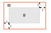
Given a level shifter , we define the bounding box of ’s net as , whose width is and height is . The -bounding box of is , which has the same centric position. Besides, width of is and height is (as shown in Fig.7).
In room , after calculating module ’s relative position, at most four rectangular white spaces are generated. We divide each white spaces into rectangular grids, whose area are all . So room records a set of grids , and each grid has its position. Level-shifters in set are sorted by area of prefer region. Smaller prefer region, higher priority. Then each level-shifter picks one grid in order.
After every level-shifter assigned choosing a grid, each level shifter in ELS chooses one free grid to insert(as shown in Algorithm 2).
| Benchmark | Max Power | Power Cost | PNR | LS Number | W.S(%) | Time(s) | |||||
| [5] | VLSAF | [5] | VLSAF | [5] | VLSAF | [5] | VLSAF | [5] | VLSAF | ||
| n10 | 216841 | 216840 | 189142 | 965 | 1007 | 0 | 9 | 4.87 | 9.44 | 6.001 | 3.24 |
| n30 | 205650 | 190717 | 146483 | 1369 | 1436 | 57 | 25 | 9.03 | 11.32 | 115.07 | 35.11 |
| n50 | 195140 | 172884 | 135316 | 1514 | 1460 | 119 | 114 | 21.10 | 16.66 | 569.36 | 116.97 |
| n100 | 180022 | 179876 | 123526 | 1671 | 1354 | 92 | 153 | 34.07 | 26.71 | 1768 | 688.13 |
| n200 | 177633 | 174818 | 130050 | 2040 | 1763 | 399 | 203 | 46.52 | 29.66 | 4212 | 1969.12 |
| n300 | 273499 | 219492 | 234389 | 2147 | 1997 | 452 | 337 | 44.10 | 37.74 | 4800 | 2392.8 |
| Avg | - | 192438 | 159818 | 1617.7 | 1502.8 | 186 | 140.2 | 26.61 | 21.92 | 1911.74 | 857.56 |
| Diff | - | - | -17% | - | -7.2% | - | -24.7% | - | -17.6% | - | -55.2% |
| Wire Length w. LS | ILO(%) | W.S(%) | Time(s) | |||||
| VLSAF | VAF+LSI | VLSAF | VAF+LSI | VLSAF | VAF+LSI | VLSAF | VAF+LSI | |
| n10 | 13552 | 17937 | 0.89 | 2.29 | 9.44 | 10.46 | 3.24 | 2.09 |
| n30 | 44225 | 43282 | 0.31 | 0.85 | 11.32 | 10.75 | 35.11 | 23.13 |
| n50 | 92678 | 95666 | 1.20 | 2.27 | 16.66 | 18.12 | 116.97 | 39.81 |
| n100 | 185622 | 191522 | 1.03 | 2.40 | 26.71 | 26.40 | 688.13 | 327.01 |
| n200 | 366003 | 365792 | 1.64 | 4.28 | 29.66 | 30.06 | 1969.12 | 1304.3 |
| n300 | 560042 | 600348 | 0.67 | 1.37 | 37.74 | 35.36 | 2392.8 | 1772.03 |
| Avg | 210404 | 219091 | 0.96 | 2.24 | 21.92 | 21.86 | 857.56 | 578.06 |
| Diff | - | +4% | - | +133% | - | -0.3% | - | -32.5% |
|
|
|
|
|
|
|
|
|
|
|
|
||||||||||||||||||||||||||||
|---|---|---|---|---|---|---|---|---|---|---|---|---|---|---|---|---|---|---|---|---|---|---|---|---|---|---|---|---|---|---|---|---|---|---|---|---|---|---|---|
| n10 | 3 | 163352 | 16386 | 10 | 0.13 | 11.58 | 3.03 | n100 | 3 | 131394 | 180023 | 150 | 0.50 | 26.8 | 438.05 | ||||||||||||||||||||||||
| 4 | 162794 | 16474 | 11 | 0.12 | 11.54 | 3.96 | 4 | 120885 | 181280 | 167 | 0.34 | 26.07 | 414.7 | ||||||||||||||||||||||||||
| n30 | 3 | 139466 | 45103 | 42 | 0.32 | 15.85 | 20.82 | n200 | 3 | 112801 | 331627 | 242 | 0.55 | 35.44 | 1949.4 | ||||||||||||||||||||||||
| 4 | 138463 | 45388 | 42 | 0.21 | 17.63 | 19.83 | 4 | 117538 | 344111 | 248 | 0.46 | 34.84 | 2036.4 | ||||||||||||||||||||||||||
| n50 | 3 | 132199 | 94105 | 130 | 0.37 | 22.72 | 51.10 | n300 | 3 | 218636 | 556718 | 389 | 0.44 | 37.14 | 2390.2 | ||||||||||||||||||||||||
| 4 | 133564 | 93296 | 151 | 0.50 | 22.95 | 49.35 | 4 | 206354 | 568364 | 417 | 0.53 | 38.54 | 2377.2 |
Given , for each level shifter in , we construct a -bounding box, called (step 6). Then we find all free grids in (step 7). In step 9, we construct bipartite graphs, then we use Hungarian algorithm to find maximum bipartite matching, which takes O(mn) time111 is the number of edges, and is the number of nodes(step 10). In step 11, we update , and remove level shifters that have been inserted. If there still are level shifters in , we update and go back to step 6.
After InsertELS(), in room , if not all the grids are inserted by level shifter, module may remove. If is in lowest voltage, it removes toward left and down to reduce total area. Otherwise, it removes toward the center of power network to minimize power network resource.
4 EXPERIMENTAL RESULTS
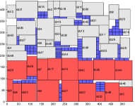
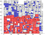
We implemented algorithm VLSAF in the C++ programming language and executed on a Linux machine with a 3.0GHz CPU and 1GB Memory. Fig. 8 shows the experimental results of the benchmarks n50 and n200. Blocks in the same voltage are nearly clustered together to reduce the power-network resource, and level shifters (small dark blocks) are inserted in white spaces. Cost function in simulated annealing is:
where and represent the floorplan area and wire length; represents the total power consumption; represents the power network resource; and records the number of level shifters that can not be assigned.
The previous work [5] is the recent one in handling floorplanning problem considering voltage assignment and level-shifter insertion. To compare with [5], we performed our experiments on the same test cases, which are based on the GSRC benchmarks adding power and delay specifications. Table shows comparisons between our experimental result and [5]. The column Power Cost means the actual power consumption, column PNR means power network resource consumption and the column W.S means white space. VLSAF can save 17% power and 7.2% PNR. The White Space and Run Time results show our framework is about 2X faster while white space can be saved by 17.6%.
We further demonstrated the effectiveness of our approach by performing another contrastive approach VAF+LSI, which solves level-shifter assignment and insertion only at post-floorplan stage. Table compares VLSAF and VAF+LSI. We can see that in VAF+LSI, although runtime is shorter(no iterative level shifter assignments during floorplanning), wire length and interconnect length overhead(ILO) are increased by 4% and 133%. High ILO may cause delay estimation among modules inaccurate, or even lead to timing constraint violation. Accordingly, VLSAF is effective and significant with a reasonable more runtime.
Besides, we have done two sets of experiments in which the number of legal working voltages for each module is set three and four. The detailed results are listed in Table 4.
5 CONCLUSIONS
We have proposed a two phases framework to solve voltage assignment and level shifter insertion: phase one is voltage and level-shifter assignment driven floorplanning; phase two is white space redistribution at post- floorplanning stage. Experimental results have shown that our framework is effective in reducing power cost while considering level shifters’ positions and areas.
References
- [1] David Lackey, Paul Zuchowski and J. Cohn. Managing power and performance for system-on- chip designs using voltage islands. ICCAD, pages 195–202, 2002.
- [2] M.Hamada and T.Kuroda. Utilizing surplus timing for power reduction. CICC, pages 89–92, 2001.
- [3] Xianlong Hong, Sheqin Dong. Non-slicing floorplan and placement using corner block list topological representation. IEEE Transaction on CAS, 51:228–233, 2004.
- [4] W.L.Hung, G.M.Link and J.Conner. Temperature-aware voltage islands architecting in system-on-chip design. ICCD, 2005.
- [5] W.P.Lee and Y.W.Chang. Voltage island aware floorplanning for power and timing optimization. ICCAD, pages 389–394, 2006.
- [6] J.Hu, Y.Shin and R.Marculescu. Architecting voltage islands in core-based system-on-a-chip designs. ISLPED, pages 180–185, 2004.
- [7] D.Sengupta and R.Saleh. Application-driven Floorplan-Aware Voltage Island Design. DAC, pages 155–160, 2008.
- [8] Q.Ma and F.Y.Young. Network flow-based power optimization under timing constraints in msv-driven floorplanning. ICCAD, 2008.
- [9] W.K.Mak and J.W.Chen. Voltage island generation under performance requirement for soc designs. ASP_DAC, 2007.
- [10] W.P.Lee and Y.W.Chang. An ILP algorithm for post-floorplanning voltage-island generation considering power-network planning. ICCAD, pages 650–655, 2007.
- [11] H.Wu, I.M.Liu and Y.Wang. Post-placement voltage island generation under performance requirement. ICCAD, 2005.
- [12] R.Ching and F.Y.Young. Post-placement voltage island generation. ICCAD, 2006.
- [13] R.K.Ahuja, T.L.Magnanti, and J.B.Orlin. Network Flows: Theory, Algorithms, and Applications. Prentice Hall/Pearson, 2005.
Bei Yu received the B.E degree in the Department of Mathematic from UESTC, China in 2007. He is currently a M.E. candidate in EDA lab, Department of Computer Science and Technology, Tsinghua University, China. His research interests include CAD for VLSI, floorplanning algorithms and low power design.
Sheqin Dong received the B.E. degree in Computer Science in 1985, M.S. degree in semiconductor physics and device in 1988, and Ph.D. degree in mechantronic control and automation in 1996. He is currently an associate professor of the EDA lab at the department of computer science and technology in Tsinghua University. His current research interests include CAD for VLSI, floorplanning and placement algorithms, multimedia ASIC and hardware design.
Song Chen received the B.S. degree in computer science from Xi an Jiao-tong University, China, in 2000, the M.S. and Ph.D. degrees in computer science from Tsinghua University, China, in 2003 and 2005, respectively. From August 2005 to April 2009, he had been a visiting associate at the Graduate School of IPS, Waseda University, Japan, where he is now an assistant professor. His research interests include several aspects of electronic design automation, e.g., floorplanning, placement, high-level synthesis.
Satoshi GOTO received the B.E. and M.E. degree in Electronics and Communication Engineering from Waseda University in 1968 and 1970, respectively. He also received the Dr. of Engineering from Waseda University in 1981. He is IEEE fellow, Member of Academy Engineering Society of Japan and professor of Waseda University. His research interests include LSI System and Multimedia System.