Colloidal pattern replication through contact photolithography operated in a “Talbot-Fabry-Perot” regime
Abstract
We detail on a continuous colloidal pattern replication by using contact photolithography. Chrome on quartz masks are fabricated using colloidal nanosphere lithography and subsequently used as photolithography stamps. Hexagonal pattern arrangements with different dimensions (, and nm, using colloidal particles with respective diameters) have been studied. When the mask and the imaged resist layer were in intimate contact, a high fidelity pattern replica was obtained after photolithography exposure and processing. In turn, the presence of an air-gap in between has been found to affect the projected image onto the photoresist layer, strongly dependent on the mask feature size and air-gap height. Pattern replication, inversion and hybridization was achieved for nm-period mask; no hybridization for the nm; and only pattern replication for the nm. These results are interpreted in the framework of a “Talbot-Fabry-Perot” effect. Numerical simulations corroborate with the experimental findings providing insight into the involved processes highlighting the important parameters affecting the exposure pattern. The approach allows complex subwavelength patterning and is relevant for a 3D layer-by-layer printing.
1 Introduction
Colloidal particle assisted nanostructuring has become a powerful tool in nanotechnology [1, 2, 3, 4, 5, 6, 7]. The common approach involves sacrificial use of a colloidal monolayer and subsequent pattern transfer via surface or bulk structuring. While this approach has provided valuable results and access to structuring techniques and configuration otherwise difficult to attain, the original colloidal mask is destroyed and has to be fabricated repeatedly [8, 9, 10, 11]. Many approaches have been developed for large-scale and easy assembly of colloidal particles yet the one-time use methodology renders the approach less attractive. For example, nanoimprint lithography and photolithography are of interest for industrial applications because they allow repeated utilization of the mask and continuous processing. Merging colloidal lithography with one of these techniques is interesting because the cost for the mask (master) fabrication could be diminished by using self-assembly techniques whereas the mask could be repeatedly used replicating the original colloidal pattern.
In this article, we explore this route and find that hexagonal arrangements of circular patterns can be easily produced by using colloidal-templated Cr-on-quartz photolithography mask. As such, the colloidal self-assembly is performed only once, whereas it allows the pattern photo-replication for virtually an infinite number of times. The mask feature size and arrangement are defined by the colloidal lithography mask (diameter of the pristine particles defines the spacing between apertures whereas the size reduction step sets the opening diameter). The photolithography in hard-contact mode resulted in a series of patterns, dependent on the mask feature dimensions and especially on the air-gap distance between the mask and the imaging plane (photoresist layer).
A Talbot-like effect is at the origin of those patterns. The Talbot effect, also known as the self-imaging effect, consists in periodic repetition of an image projected through a diffraction grating [12, 13, 14, 15]. When a plane wave is transmitted through a periodic diffraction grating, repetitive images of the grating itself are obtained. The Talbot distance is then defined as the distance from the source where the first regular image is projected, also called Talbot image. The Talbot imaging has a fractal nature with intermediate images appearing at smaller distances than the Talbot distance. These sub-images are characterized by smaller feature size and pattern hybridization. Moreover, some works consider the Talbot distance in photolithography. For instance, the Talbot effect can be used to produce complex 3D periodic patterns [13, 15]. Nevertheless, in the present work, while the typical Talbot distance should be in the micrometer range, we show that complex patterns occur for small air-gap distance. This is due to the fact that Cr-on-quartz mask and silicon substrate of the photoresist layer act as a Fabry-Perot cavity which squeezes the Talbot effect. In the following section II, the experimental setup is described. Results are introduced and discussed thanks to numerical simulations in section III.
2 Experimental section
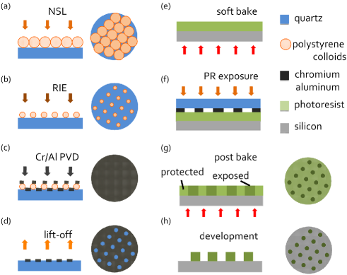
The experimental part of this work is schematized in Fig.1. Polystyrene colloidal particles with different nominal diameters have been used in this study as received (Microparticles GmbH; nm, nm and nm). Nanosphere lithography (NSL, Fig.1a) has been performed using previously documented techniques on quartz wafers [11, 16, 17]. Reactive ion etching (RIE, Fig.1b) was used to reduce the size of the spherical particles. Next, nm of metallic Cr was deposited by physical vapor deposition (PVD) followed by lift-off by adhesive tape (Figs.1c and 1d). To remove any residual organic layer, samples were sonicated in dichloromethane and exposed to a short O2 plasma ashing. At this stage, the Cr-on-quartz mask was ready for use.
For the photolithography experiments, nm of KMPR-series negative resist was coated on Si chips. In order to attain such thin photoresist films, the KMPR1025 commercially available formulation (MicroChem Corp.) was diluted (1/9 volumetric ratio) with cyclohexanone (Sigma Aldrich, b.p. 156∘C). No anti-reflective coating layer was used. Prior to the irradiation, the resist was soft-baked at ∘C for s (Fig.1e). The exposure was done using a KW Karl Süss mask aligner operated in hard-contact mode (Hg-lamp, i-line, cold mirror filtered; exposure wavelength centered at nm, W power) (Fig.1f). The exposure time was varied between and s depending on mask type. The resist was then post-baked at ∘C for s and the imaged pattern was revealed in a standard developing formulation (AZ 726 MIF) for s at ambient temperature (Figs.1g and 1h). The rather short soft-baking time ( s at ∘C) was found insufficient to completely remove the solvent and the coated films were occasionally found to be adherent and easy to indent (see further discussions). Nonetheless, the detailed protocol was found to be optimal for attaining high photolithography contrast and resolution.
Morphology characterization was performed using scanning electron microscopy (SEM, XL 30 FEG) and optical microscopy. Maps of the square modulus of the electric field are obtained from a homemade numerical code which uses a Rigorous Coupled Wave Analysis (RCWA) approach jointly with a scattering matrix method [18, 19, 20].
3 Results and discussions
3.1 Description of the procedure
A schematized view of the experimental approach used in this work is shown in Fig.1. As can be noticed, the NSL is done only once, during the mask fabrication step and the fabricated Cr-on-quartz mask is used repeatedly to replicate the NSL pattern. We have used the fabricated mask for more than 20 times without any sign of degradation. The only required precaution was the solvent rinsing of the mask after each utilization to remove the photoresist residues found to affect the quality of the photolithography process. We choose to work with NSL for mask fabrication as it allowed us to rapidly fabricate and scan the influence of the feature size of the mask (just by simply using colloids with different size) on the photolithography outcome. Furthermore, photolithography masks are usually fabricated using electron-beam lithography (especially when sub-micrometer features are targeted), which is a serial writing technique and time consuming. In contrast, colloidal lithography as a bottom-up approach can be performed over large areas, in relatively short time and at low costs. Whilst the drawback is the constrained pattern design, some applications require just periodic nano-structuring without any special pattern designs like antireflective and super-hydrophobic surfaces or mass production of nanostructures for various applications [21, 22, 23].
3.2 Mask fabrication
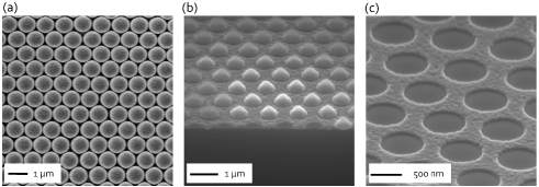
Colloidal particles monolayer with hexagonal symmetry is obtained after NSL. Top-view of an assembled monolayer composed of colloidal particles with a diameter of nm is shown in Fig.2a. After the O2 RIE step, the close-packing of the spheres is altered while the hexagonal arrangement is preserved (Figs.2b and 2c). After Cr-metal deposition and lift-off, a holey metal film is obtained. The elevation of the quartz plane with respect to the photoresist plane is expected to be of the order of nm (corresponding to the thickness of the Cr layer). It is worth mentioning here that often, photoresist residues were found on the quartz areas on mask as well as pale iridescence was observed on the photoresist layer after exposure without being developed (data not shown here). This presumably implies Cr features percolating partially into the photoresist layer or, in other words, photoresist and the quartz plane are brought in intimate contact. Hard contact mode used for the lithography step, soft nature of the photoresist layer as well as partial bake-out may be at the origin of these experimental observations. However, the thickness of the Cr layer is only nm and, as it will be shown further, the critical separation is much higher than the above mentioned value. Depending on the type of resist (positive or negative), direct or inverted replica respectively, can be obtained after exposure and revealing. Here, we have used negative tone photoresist (KMPR series). Consequently, holes of the Cr-on-quartz mask will normally yield photoresist posts after processing. To avoid thin-film interference, the thickness of the photoresist film was set to nm. As such, the pattern obtained after processing can be approximated to the plane projected image of the light passing through the holey-metal Cr-on-quartz mask.
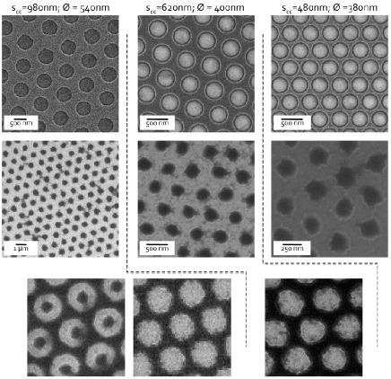
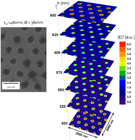
Examples of fabricated masks with different feature parameters are shown in Fig.3. Three mask types have been used, fabricated using different colloid diameters: mask M1, lattice constant nm and hole diameter nm; mask M2, nm and nm; mask M3, nm and nm. Careful inspection over the entire area of the mask showed that there are no inverted patterns (i.e. metallic dots) as well as the absence of any impurities at the center of the holes. These observations are important because the inspection of the photolithography results revealed the presence of unexpected patterns, especially for M1, not due to the presence of defects on the mask. Those surprising patterns are related to the Talbot effect, as discussed hereafter.
3.3 Lithography results
The photolithography results are shown in Fig.3 (bottom row). Arrays of resist dots have been primarily obtained, consistent with the processing conditions (openings in a Cr-on-quartz mask and negative tone photoresist). The dots have circular symmetry and preserve the hexagonal arrangement for all three types of masks. While the dot lattice spacing is fixed as defined by the imaging mask, their diameter can be modified by adjusting the exposure dose and post processing parameters (developer concentration and time). Using M3 mask (Fig.3, bottom row), the diameter of the dots is close to the resolution limit of nm. Indeed, as shown hereafter, the photoresist layer is still located in the radiative near-field zone - i.e. the Fresnel zone - and not in the non-radiative near-field region. As such, simple mask fabrication procedure combined with standard photolithography enabled fast and large-area replication of nm features.
Another interesting finding was the observation of inverted and multiplied (along with normal) patterns after photolithography processing. Examples are shown in the bottom row of Fig.3. Such feature was not observed for the mask M3 for which only photoresist posts were obtained. Using mask M2, pattern inversion was observed: instead of obtaining photoresist posts, holes in the photoresist films were obtained. Furthermore, three types of patterns were obtained using the M1 mask: normal - photoresist posts, inverted - holey photoresist film and a combination of both - i.e., holey films with posts at the interior of hole (donut-like structures). It should be noted here that even though hard contact mode photolithography was used, due to the processing defects and non-planarity of both mask and carrier sample, conformal contact between both elements was not possible to achieve over the entire area of the sample. The presence of an air-gap in between was visually identified by the appearance of the interference patterns (however, limited to less than of the entire sample area). The above-mentioned pattern shape anomalies were mainly observed in the respective areas and seemingly attributed to the air-gap. We did not performed any extended experiment to precisely control the gap-spacing between the imaging (Cr-on-quartz mask) and the imaged (photoresist layer) planes. While this could be implemented easily by deposition of a transparent dielectric layer [13] of desired thickness either on mask or on top of the photoresist, we centered our interest in numerically interpreting the obtained results and finding the critical parameters that affect the photolithography processing outcome [15].
3.4 Modeling
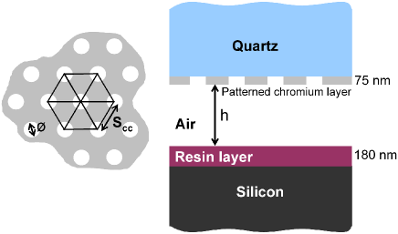
Simulations provide the square modulus of the electric field (i.e. the field intensity) and are obtained from a homemade numerical code which uses a RCWA approach jointly with a scattering matrix method [18, 19, 20]. The simulation configuration is depicted in Fig. 4. The Cr-on-quartz mask is numerically represented as an opaque film bearing hexagonally arranged holes. The thickness of the Cr layer is set to nm while the quartz is being considered of infinite thickness. Similarly, the silicon supporting substrate is simulated of infinite thickness while the photoresist is -nm-thick. The air-gap () is defined as the distance between the upper surface and lower boundary of the photoresist and Cr layer, respectively. Assuming that nm, the optical constant of the materials are as follows: , , , for chromium, quartz, silicon, [24] and resin (KMPR) respectively. In each figure, is the separation between the chromium/air and the resin/air interfaces in the modelized system (see Fig.4). In each figure, the electromagnetic field intensity scales are given for an incident electric field (in quartz substrate) equal to Vm-1.
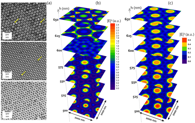
Fig.5 shows the simulation and experimental results for process using mask M1. For an air-gap of nm or below, direct imaging is observed, i.e. arrays of photoresist posts (bottom SEM image). It should be mentioned that no other patterns were observed in the respective areas. Simulation shows that the reversed pattern (middle SEM image) is obtained for around nm whereas the hybridized pattern (top SEM image) is recovered for about nm. All other values were found to recover the bottom SEM image. Interestingly, a small variation in ( nm) is found to dramatically affect the projected image requiring precise mask and air-gap engineering/design if the respective patterns are targeted. Close inspection of the inverted and hybridized pattern area revealed intermixing of the respective patterns within. For example, in the inverted pattern (holey polymer film), occasionally, polymer posts were found in the middle of the hole and inversely, the absence of the polymer post was observed in the hybridized pattern (marked with arrows in Fig.5). The very small separation required to differentiate the two patterns and possible non-uniformities of the mask features (for example, small variation in the colloid size leading to different hole size) are the reason for the pattern mixing.
Fig.5c shows the simulation results for conditions similar to those presented in Fig.5b, except that the silicon substrate and the resin layer were numerically removed in order to propagate the electromagnetic field in true Talbot conditions [15]. We clearly see that the electromagnetic field patterns strongly differ from those obtained in Fig.5b. This shows that the present experimental results depend on the interferences between the electromagnetic wave arising from the chromium mask and the reflected wave on the silicon-resin interface, which acts as a mirror. It should be noted that, in the experiments, no anti-reflective layer was used on silicon substrate. Eventually, using such a layer would eliminate the mirror-cavity interferences and lead to direct pattern replication without any special care with respect to the air-gap height [13].
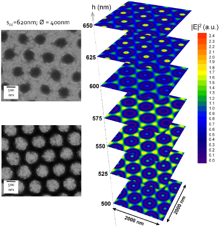
Having confirmed the applicability of the simulation protocol to the observed experimental results, we have analyzed the results obtained using masks M2 and M3. Fig.6 shows the experimental results obtained using mask M2 and the corresponding simulated electromagnetic field intensity at the surface of the photoresist layer. The inverted pattern, i.e. holey photoresist film (bottom SEM image), is roughly recovered for between and nm. The top SEM image (the normal pattern) is obtained for the other values (higher than nm and lower than nm). The pattern mixing was not observed here, neither experimentally nor in the simulations. The results for mask M3 are shown in Fig.7. In this configuration, only direct patterning was observed. Polymer posts were obtained independently of the value.
| 751 | 730 | 750 | |
| 536 | 548 | 550 | |
| 417 | - | - | |
| 341 | 365 | 350 | |
| 289 | - | - | |
| 250 | - | - | |
| 221 | - | - | |
| 198 | - | - | |
| 179 | 183 | 200 | |
| 456 | 548 | Undefined | |
| 274 | 365 | 350 | |
| 196 | 183 | 200 | |
| 700 | 730 | Undefined | |
| 233 | 183 | Undefined |
3.5 Discussions
As previously mentioned, the Talbot effect consists in periodic repetition of an image of a diffraction grating [12, 13, 14]. The Talbot distance is the distance between the source and the first regular image. The Talbot imaging presents intermediate images appearing at smaller distances than the Talbot distance. These sub-images are characterized by smaller feature size and pattern hybridization. The Talbot distance () can be approximated using the following equation provided that light propagates in air [14]:
| (1) |
where is the incident wavelength, is the grating lateral period (, with the lattice period of the mask). For the experimental set-up and the three different masks used in this study, values are as follows: for mask M1, m; for mask M2, m; and for M3, m. These large values lead to almost constant patterns when the distance between mask and photoresist slowly varies, as shown in Fig.6. Nevertheless, in the present case, the silicon substrate dramatically modifies the lateral pattern behavior. Indeed, the Cr-on-quartz mask and the silicon-photoresist support act as a Fabry-Perot cavity allowing for fast lateral pattern variation when varies. Since the silicon acts as a mirror, we can fairly suppose that the new Talbot distance (squeezed Talbot distance) will be given by where is an integer. Indeed, with , which means that the Talbot distance is retrieved with , i.e. when light has made trips between the source (the mask) and the mirror (the silicon substrate). An odd number of trips is required to get the final image of the source on the mirror. For each mask, the values of are shown in Table 1. In addition, the Fabry-Perot implies that the distance for which the field can resonantly propagate between both plates is given by ( is an integer different from zero). Those values can be compared with the theoretical squeezed Talbot distance as shown in Table 1. Then, for each mask, we can compare the numerically computed squeezed Talbot distance with the relevant values of (see Table 1).
For masks M1 and M2, this approach matches quite well. For mask M3, we are closer to the true Talbot conditions and we lose the capability to get complex subwavelength patterns. Typical air-gap widths are between et nm, i.e. and , and the mask pattern is retrieved all along those distances. Pattern deformation during photolithography induced by the presence of mask-substrate gaps is a known phenomenon and several studies have analyzed this effect and solutions to compensate the distortions have been proposed [25]. The major difference with respect to data presented in this work is that the air-gaps utilized in previous reports as well as characteristic feature dimensions were far much higher than the exposure wavelength. The documented distortions were attributed to the divergence of the exposure source (in the combined optical system made of light source/mask/photoresist plane). Moreover, in our case, the characteristic dimensions are of the order of the wavelength and the source divergence is expected to have a minimal influence on the results. At last, note that, even though the real part of the Cr permittivity is negative here, surface plasmons cannot be excited. Indeed, since the incident light is at normal incidence, any surface plasmon excitation is due to diffraction orders which become tangent to the metallic surface. In the present case, for the hexagonal lattice, no orders can provide a resonant excitation for wavelengths in the very close “vicinity” of nm whatever the lattice parameter. As a consequence, surface plasmons play no role in the present study.
4 Conclusions
We have introduced a continuous colloidal pattern replication using contact photolithography thanks to a Talbot-like effect. Cr-on-quartz masks have been fabricated using nanosphere lithography and used as photolithography stamps. Dimensions of the pattern are experimentally controllable (initial size of the colloids, the etching procedure, etc.). Hexagonal pattern arrangements with different dimensions have been considered. Depending on the thickness of the air-gap between the mask and the photoresist layer, various changes occur in the pattern replica. The present approach then allows to obtain complex bidimensional patterns at a subwavelength scale. For instance, not only dots can be obtained (high fidelity replica of the mask), but also subwavelength anti-dots or rings. As a consequence, this patterning approach benefits from the “infinite” use of the mask while allowing multi-pattern with a single mask. Numerical simulations and a simple model allow to predict the obtained patterns against the air-gap thickness. Further improvements could be considered with a piezoelectric actuator allowing for an accurate control of the air-gap and, then, of the obtained patterns. This could also allow 3D layer-by-layer printing.
A.V. acknowledges F.R.S.-FNRS for financial support. This research used resources of the “Plateforme Technologique de Calcul Intensif (PTCI)” (http://www.ptci.unamur.be) located at the University of Namur, Belgium, which is supported by the F.R.S.-FNRS under the convention No. 2.4520.11. The PTCI is member of the “Consortium des Équipements de Calcul Intensif (CÉCI)” (http://www.ceci-hpc.be).
References
References
- [1] T. Kraus, D. Brodoceanu, N. Pazos-Perez, A. Fery, Colloidal Surface Assemblies: Nanotechnology Meets Bioinspiration, Advanced Functional Materials 23 (2013) 4529.
- [2] C.G. Schäfer, M. Gallei, J.T. Zahn, J. Engelhardt, G.P. Hellmann, M. Rehahn, Reversible Light-, Thermo-, and Mechano-Responsive Elastomeric Polymer Opal Films, Chemistry of Materials 25 (2013) 2309-2318.
- [3] J. Zhang, Y. Li, X. Zhang, B. Yang, Colloidal Self-Assembly Meets Nanofabrication: From Two-Dimensional Colloidal Crystals to Nanostructure Arrays, Advanced Materials 22 (2010) 4249-4269.
- [4] H. Fredriksson, Y. Alaverdyan, A. Dmitriev, C. Langhammer, D.S. Sutherland, M. Zäch, et al., Hole-Mask Colloidal Lithography, Advanced Materials 19 (2007) 4297-4302.
- [5] H. Zhang, P.V. Braun, Three-Dimensional Metal Scaffold Supported Bicontinuous Silicon Battery Anodes, Nano Letters. 12 (2012) 2778 2783.
- [6] S. Kim, S. Lee, S. Yang, G.-R. Yi, Self-assembled colloidal structures for photonics, NPG Asia Materials 3 (2011) 25-33.
- [7] J. Zhang, B. Yang, Patterning Colloidal Crystals and Nanostructure Arrays by Soft Lithography, Advanced Functional Materials 20 (2010) 3411-3424.
- [8] N. Vogel, L. De Viguerie, U. Jonas, C.K. Weiss, K. Landfester, Wafer-Scale Fabrication of Ordered Binary Colloidal Monolayers with Adjustable Stoichiometries, Advanced Functional Materials 21 (2011) 3064-3073.
- [9] S.P. Bhawalkar, J. Qian, M.C. Heiber, L. Jia, Development of a Colloidal Lithography Method for Patterning Nonplanar Surfaces, Langmuir 26 (2010) 16662-16666.
- [10] H.-P. Wang, K.-Y. Lai, Y.-R. Lin, C.-A. Lin, J.-H. He, Periodic Si Nanopillar Arrays Fabricated by Colloidal Lithography and Catalytic Etching for Broadband and Omnidirectional Elimination of Fresnel Reflection, Langmuir 26 (2010) 12855-12858.
- [11] A. Vlad, A. Frölich, T. Zebrowski, C.A. Dutu, K. Busch, S. Melinte, et al., Direct Transcription of Two-Dimensional Colloidal Crystal Arrays into Three-Dimensional Photonic Crystals, Advanced Functional Materials 23 (2013) 1164-1171.
- [12] J. Wen, Y. Zhang, M. Xiao, The Talbot effect: recent advances in classical optics, nonlinear optics, and quantum optics, Adv. Opt. Photon. 5 (2013) 83.
- [13] C.H. Chang, L. Tian, W.R. Hesse, H. Gao, H.J. Choi, J.G. Kim, et al., From Two-Dimensional Colloidal Self-Assembly to Three-Dimensional Nanolithography, Nano Letters 11 (2011) 2533-2537.
- [14] J.T. Winthrop, C.R. Worthington, Theory of Fresnel Images I Plane Periodic Objects in Monochromatic Light, J. Opt. Soc. Am. 55 (1965) 373.
- [15] T. Sato, High-Order Approximation of the Talbot Distance for Lithography, Appl. Phys. Express 5 (2012) 092501.
- [16] A. Vlad, I. Huynen, S. Melinte, Wavelength-scale lens microscopy via thermal reshaping of colloidal particles, Nanotechnology 23 (2012) 285708.
- [17] N. Reckinger, A. Vlad, S. Melinte, J.-F. Colomer, M. Sarrazin, Graphene-coated holey metal films: tunable molecular sensing by surface plasmon resonance, Applied Physics Letters 102 (2013) 211108.
- [18] M. Sarrazin, J.-P. Vigneron, J.-M. Vigoureux, Role of Wood anomalies in optical properties of thin metallic films with a bidimensional array of subwavelength holes, Phys. Rev. B 67 (2003) 085415.
- [19] J.-P. Vigneron, V. Lousse, Variation of a photonic crystal color with the Miller indices of the exposed surface, Proc. of SPIE. 6128 (2006) 61281G.
- [20] J.-P. Vigneron, F. Forati, D. André, A. Castiaux, I. Derycke, A. Dereux, Theory of electromagnetic energy transfer in three-dimensional structures, Ultramicroscopy 61 (1995) 21-27.
- [21] J.-J. Kim, Y. Lee, H. Kim, K.-J. Choi, H.-S. Kweon, S. Park, K.-H. Jeong, Biologically inspired LED lens from cuticular nanostructures of firefly lantern, Proc. Natl. Acad. Sci. 109 (2012) 18674.
- [22] A. Vlad, A.L.M. Reddy, A. Ajayan, N. Singh, J.-F. Gohy, S. Melinte, P.M. Ajayan, Roll up nanowire battery from silicon chips, Proc. Natl. Acad. Sci. 109 (2012) 15168.
- [23] K.-C. Park, H.J. Choi, C.-H. Chang, R.E. Cohen, G.H. McKinley, G. Barbastathis, Nanotextured silica surfaces with robust superhydrophobicity and omnidirectional broadband supertransmissivity, ACS Nano 6 (2012) 3789.
- [24] E.D. Palik, Handbook of Optical Constants of Solids II, 1997 Elsevier Inc. (1997).
- [25] W. J. Venstra, J.W. Spronck, P. M. Sarro, J. van Eijk, Photolithography on bulk micromachined substrates, J. Micromech. Microeng. 19 (2009) 055005.