Study on the tunneling spectroscopy of junction and junction
Abstract
We study the complete tunneling spectroscopy of a normal metal/-wave superconductor junction () and normal metal/heterostructure superconductor junction () by Blonder-Tinkham-Klapwijk (BTK) method. We find that, for -wave superconductor with non-trivial topology, there exists a quantized zero-bias conductance peak stably, for heterostructure superconductor with non-trivial topology, the emerging zero-bias conductance peak is non-quantized and usually has a considerable gap to the quantized value. Furthermore, it is sensitive to parameters, especially to spin-orbit coupling and the -wave pairing potential. Results obtained suggest that the observation of a small zero-bias conductance peak, instead of a quantized zero-bias conductance peak, in current tunneling experiments can be a natural result if the spin-orbit coupling turns out to be several times smaller than the reported one. Results obtained also suggest that both a stronger spin-orbit coupling and proximity -wave superconductor with relative weaker pairing potential can produce a much more striking zero-bias conductance peak (compared to the experiments), even an almost quantized one. As -wave superconductors are common in nature, the prediction can be verified within current experiment ability.
pacs:
73.63.Nm, 14.80.Va, 05.30.Rt, 71.70.EjI Introduction
Because of hosting exotic non-abelian zero modes D. A. Ivanov which have great potential in topological quantum computation A. Kitaev1 ; S. Das. Sarma ; C. Nayak , -wave superconductor either in two dimension N. Read or in one dimension A. Kitaev2 has raised strong and lasting interests for more than a decade. Although there is no definite confirmation of -wave superconductor in solid state physics A. P. Mackenzie ; C. Kallian , several groups Liang Fu1 ; Jay D. Sau ; Roman M. Lutchyn ; Y. Oreg ; J. Alicea1 ; A. C. Potter , based on proximity effect, have proposed a series of heterostructures whose common elements are spin-orbit coupling, -wave superconducting order and Zeeman field and found, by tuning parameters, the upper band of the system can be projected away, and the Copper pairs formed in the lower band is “effective -wave”, and for such an “effective -wave” superconductor, the zero modes known as Majorana bound states emerge at defects or the boundary of the system. Such heterostructures with non-trivial topology is known as topological superconductors.
To detect the Majorana bound states, there are mainly three classes of measurements schemes J. Alicea2 ; T. D. Stanescu , based on tunneling K. Sengupta ; C. J. Bolech ; Johan Nilsson ; Liang Fu2 ; A. Akhmerov ; K. T. Law ; Karsten Flensberg ; Stefan Walter ; Dong E. Liu ; A. R. Akhmerov ; R. Zitko ; Y. Cao ; S. Mi ; Z. Wang , fractional Josephson effects P. A. Ioselevich ; Liang Jiang ; Pablo San-Jose ; L. Jiang ; Fernando Dominguez and interferometry Colin Benjamin ; Chao-Xing Liu ; Andrej Mesaros . Recently, several tunneling experiments V. Mourik ; A. Das ; M. T. Deng ; A. D. K. Finck based on the proposals of one-dimensional topological superconductors Roman M. Lutchyn ; Y. Oreg were carried out and all these experiments found that a zero-bias conductance peak, which is taken as a signature of Majorana bound states, emerges in the tunneling spectroscopy when the magnetic field along the nanowire exceeds the critical value, , . However, it is also noticed that the peak height is quite small, having a big discrepancy to the theoretical prediction: a quantized zero-bias peak of height (at zero temperature) K. Sengupta ; K. T. Law ; Karsten Flensberg . The big discrepancy has raised debate on the origin of the zero-bias conductance peak. To understand the experiments and clarify the origin of the peak, a series of work E. Prada ; Tudor D. Stanescu ; C.-H. Lin ; E. J. H. Lee ; G. Kells ; J. Liu ; D. Bagrets ; D. I. Pikulin ; D. Rainis ; D. Roy have been carried out, and some of the work point out that the non-quantized zero-bias conductance peak can have several other origins, like Kondo effect E. J. H. Lee , smooth end confinement G. Kells , strong disorder J. Liu ; D. Bagrets ; D. I. Pikulin , and suppression of the superconducting pair potential at the end of the heterostructure D. Roy . Therefore, a definite confirmation of Majorana bound states is still lacking. As the heterostructures are proposed to be an “effective -wave” superconductor, a comparative study of the tunneling spectroscopy of a normal metal/-wave superconductor () junction and normal metal/heterostructure superconductor () (here we name the heterostructure as heterostructure superconductor, instead of topological superconductor, since it can also be topologically trivial) junction to see what extent the “effective” can reach is important and valuable, for both understanding of the realized experiments and giving some guide for future experiments.
In this article, according to the BTK method G. E. Blonder , we systematically consider the effects due to (i) the length () of the system, (ii) interface scattering potential (), (iii) chemical potential mismatch (), to the tunneling spectroscopy of both junctions, and only consider the effects due to (iv) spin-orbit coupling (), (v) magnetic field () along the wire, (vi) -wave pairing potential, to the tunneling spectroscopy of junction. For junction, we obtain a complete tunneling spectroscopy analytically, including probability of normal reflection (an electron reflected as an electron with the same spin), probability of equal-spin Andreev reflection (an electron reflected as a hole with the same spin), and the differential tunneling conductance and their dependence on system parameters. For junction, we obtain the complete tunneling spectroscopy numerically, including probability of normal reflection, probability of spin-reversed normal reflection (an electron reflected as an electron with the opposite spin), probability of spin-reversed Andreev reflection (an electron reflected as a hole with the opposite spin), probability of equal-spin Andreev reflection and the differential tunneling conductance and their dependence on parameters. Although only the differential tunneling conductance is observable in experiments, the other reflection coefficients are also very important for us to understand the underlying tunneling process. Among these reflection coefficients, spin-reversed Andreev reflection and equal-spin Andreev reflection are worthy of attention, they can tell us whether the system favors -wave pairing or -wave pairing, and give a quantitative estimate of the extent the “effective” has reached.
The main results obtained, for junction: (a) When and is sufficiently long, the zero-bias peak is always quantized, of height () and independent of , however, once crosses zero and becomes negative, , , the zero-bias conductance peak changes into a conductance dip, with value very close to zero, which indicates there exists a topological quantum transition when crosses zero. (b) When is short, the conductance is very close to zero and no conductance peak appears both for and . However, when is increased to intermediate value, a non-quantized conductance peak appears at finite energy for and with the increase of , the peak moves toward to zero-bias voltage with height increasing to the quantized value. For junction: (a) With infinity length, we find when the magnetic field crosses the critical value , a zero-bias peak appears, however, unlike the -wave case, the peak height is non-quantized, and parameters dependent. (b) Decreasing the spin-orbit coupling will reduce the height of the zero-bias conductance peak, and when the spin-orbit coupling decreases to zero and other parameters keep unchanged, the zero-bias conductance peak disappears, which indicate the breakdown of the usual topological criterion for a heterostructure superconductor. When is intermediate, similar to junction, there is also a non-quantized conductance peak appearing at finite energy for . (c) Adopting the experimental parameters, we study the effects of the -wave pairing potential and find that a more striking zero-bias conductance peak favors a weaker pairing potential. Furthermore, we find that the spin-orbit coupling several times smaller than the reported one in the experiment V. Mourik which can be taken as a possible explanation of the quite small zero-bias conductance observed in the experiment.
The paper is organized as follows: In Sec.II, we give the theoretical models for junction and junction explicitly, and based on the BTK method G. E. Blonder , we obtain the tunneling spectroscopy of junction and junction under different parameter conditions. In Sec.III, we give a discussion of the tunneling spectroscopy of junction and junction obtained in Sec.II. We also conclude the paper at the end of Sec.III.
II Theoretical model
II.1 junction
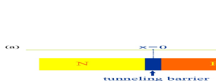
We first consider the one-dimensional junction shown in Fig.1(a). Under the representation , the Hamiltonian is given as
| (1) |
where are pauli matrices, is the scattering potential at the interface, is potential induced by disorder, external field, , for junction, we set . is the chemical potential, we set for and for , is the chemical mismatch. is the pairing potential, we assume it only appears at .
For , the -wave superconductor, the Hamiltonian in momentum space is given as (in the following, we set )
| (2) |
which is the continuum form of the Kitaev model A. Kitaev2 . Its energy spectrum is . As we know, the energy gap is only closed at , and for , the system is topologically non-trivial (trivial).
To study the behavior of tunneling spectroscopy when goes across the critical point , we consider , where is very close to and the minimum of the energy spectrum is located at . For a given energy (here we only consider in-gap states, , , as the differential tunneling conductance at zero-bias voltage is what we are the most interested in), the wave function in -wave superconductor is given as
| (7) | |||||
| (12) |
where , , and . , , and are energy-dependent coefficients, and when , , it is obvious that the wave function is localized at the left end of the wire.
For , the normal metal lead, the Hamiltonian is,
| (13) |
here we keep for convenience. We consider that an electron is injected from the normal lead into the -wave superconductor, and the wave function in the normal lead is given as
| (18) |
where . and denote equal-spin Andreev reflection amplitude and normal reflection amplitude, respectively.
Following the BTK methods G. E. Blonder , the two wave functions (12) and (18) need to satisfy the boundary conditions,
| (19) |
where , and , two matrices, are the velocity operators L. W. Molenkamp . From Eq.(19), we can obtain and directly, and according to Ref.G. E. Blonder , the zero-temperature differential tunneling conductance is given as
| (20) |
where , (), is the equal-spin Andreev reflection probability, and is the normal reflection probability. Here as we only consider in-gap states, the waves expressed in Eq.(12) do not carry current, and and satisfy the normalization condition, , . For different parameters , and (we set as unit), the results are shown in Fig.2.
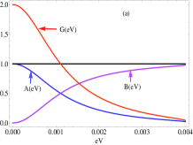
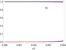
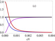
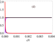
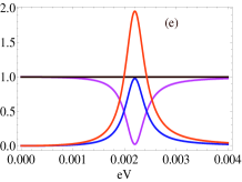
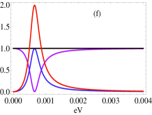
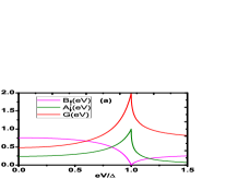
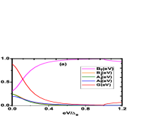
Fig.2(a) and Fig.2(b) show the important difference of differential tunneling conductance between (topologically non-trivial) and (topologically trivial). For , a quantized zero-bias conductance peak of stably exists (as shown in Fig.2(a)(c)(d)). A stable and quantized zero-bias conductance peak is a manifestation of perfect equal-spin Andreev reflection and indicates a stable topological phase. This result is the same as the one obtained by an “interface electron-Majorana hopping” model K. T. Law ; Karsten Flensberg , therefore, even we do not, in prior, assume the existence of the Majorana bound states at the wire end, the non-trivial topology of the -wave superconductor manifest itself in the tunneling spectroscopy obtained by matching the wave functions of the two bulks directly. For , the in-gap differential tunneling conductance almost vanishes. The important difference indicates that, for -wave superconductor, the tunneling experiments can detect the topological quantum transition at effectively. Fig.2(c) and Fig.2(d) show that increasing the interface scattering potential only narrows the width of the peak, neither changes the quantized height (an analytical proof for it is given in the Appendix) nor the position of the peak. The wire length has strong impact on the conductance for , as shown in Fig.2(e) and Fig.2(f), for and , the conductance peaks appear at finite-bias voltage and the peak will move toward to left (zero-bias voltage) with increasing (this agrees with the usual two end-Majoranas coupled picture). The effect of the interface scattering potential for finite length is similar to the one mentioned above. For sufficiently short , for example, , there is no conductance peak and the in-gap differential tunneling conductance almost vanishes. For , the topologically trivial phase, the wire length and the interface scattering potential has little effect, the in-gap differential tunneling conductance keeps very small.
Above we have restricted to be close to , and there is a big mismatch between and . Canceling this restriction, we find, for , increasing greatly widens the width of the zero-bias peak of the in-gap tunneling spectroscopy, however, the peak’s quantization behavior does not change and therefore the main physics does not change. For , decreasing has little effect to the in-gap tunneling spectroscopy.
II.2 junction
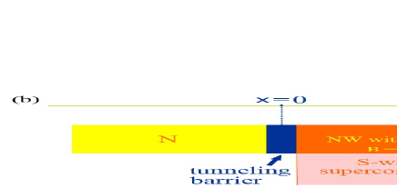
The one-dimensional junction is shown in Fig.1(b). For , the Hamiltonian is a generalized matrix form of Eq.(13). For , now the Hamiltonian is given as Roman M. Lutchyn (in momentum space, under representation )
| (21) |
where , is the in-plane magnetic field along the wire, is the spin-orbit coupling strength, and is the -wave pair potential. and are pauli matrices in particle-hole space and spin space, respectively. The heterostructure described by this Hamiltonian is just the one that is realized in the experiment V. Mourik . The quasiparticle energy spectrum is given as
the energy gap is closed when the magnetic field reaches the critical value , which separates , the topologically trivial phase, from , the topologically non-trivial phase. The energy-momentum relation here is much more complicated than the -wave superconductor’s. This complication makes us unable to write down the analytical form of the wave function directly, and have to seek help from numerical tools.
As the Hamiltonian (21) is a matrix, the wave function in the normal metal is a four-component vector, which takes the form,
| (34) |
where denotes the normal reflection amplitude, denotes the spin-reversed reflection amplitude, denotes the equal-spin Andreev reflection amplitude, and denotes the spin-reversed Andreev reflection amplitude. Now the boundary conditions take the form
| (35) |
where is a matrix, and is also generalized to matrix.
Based on Eq.(35), we can obtain and , and the differential tunneling conductance is given as
| (36) |
where , and . and in the gap region should satisfy the normalization condition: . For different parameters, the results are shown in Fig.3.
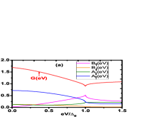
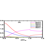
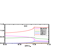
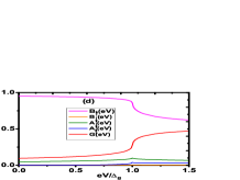
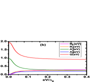
Fig.3(a)(b) show when , the topological region, a zero-bias conductance peak is formed. However, contrary to the quantized zero-bias conductance peak of a junction, here the zero-bias peak is non-quantized and sensitive to parameters. Increasing the interface scattering potential not only narrows the width of the peak but also increases the height of the peak. From Fig.3(a)(b), we can also see the increase of the peak height is due to a suppression of the spin-reversed Andreev reflection and a simultaneous increase of the equal-spin Andreev reflection by the interface scattering potential. However, with a further increase of the interface scattering potential, this corresponding increasing effect will finally be saturated, and the zero-bias conductance peak still has a gap to the quantized value.
For comparison, Fig.3(c)(d) show when , the normal phase, no zero-bias peak appears, and by increasing the interface scattering potential, the normal reflection is greatly enhanced and the spin-reversed Andreev reflection and the conductance are greatly reduced, which is a phenomenon familiar in junctions G. E. Blonder . Compared Fig.3(a)(b) to Fig.3(c)(d), it is not hard to find that when the system goes from the normal phase to the topological phase, the probability of equal-spin Andreev reflection is greatly enhanced (but still has a considerable gap to the perfect equal-spin Andreev reflection) and the spin-reversed Andreev reflection amplitude is greatly reduced, which indicates the equal-spin pairing (-wave pairing) becomes much more favored in the topological region than in the normal region.
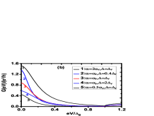
Spin-orbit coupling also has strong impact on the tunneling spectroscopy. As shown in Fig.4(a), when decreasing the spin-orbit coupling and fixing other parameters, the height of the zero-bias peak and the probability of equal-spin Andreev reflection are significantly reduced. A further inspection shows that once the spin-orbit coupling decreases to a critical value (named as ) not only the peak height keeps decreasing to a smaller value but also the induced gap begins to depend on spin-orbit coupling (when , we say the spin-orbit coupling is weak), with a dependence that it monotonically decreases with decreasing spin-orbit coupling. When the spin-orbit coupling is decreased to zero, the induced gap gets closed, the system turns to be gapless and the zero-bias conductance peak disappears, which indicates a breakdown of the topological criterion
As above, we show that decreasing the spin-orbit coupling (from the Fig.3’s parameter, ) lowers the peak, we find that increasing the spin-orbit coupling does not correspond to a monotonic increase of the peak height. As shown in Fig.4(b)(c), the zero-bias conductance peak first increases and then decreases with increasing spin-orbit coupling, the optimal spin-orbit coupling under the parameters given in Fig.4(c) is about . In the following, when , we say the spin-orbit coupling is in the intermediate region, and when , we say the spin-orbit coupling is strong. From Fig.4(c), we also find when goes beyond , a larger corresponds to a lower peak and the reduction effect due to the increase of spin-orbit coupling is significant. However, we also find, almost simultaneously when goes beyond , the saturation effect of the interface scattering potential for weak spin-orbit coupling is absent, and a stronger interface potential will induce a higher peak, as shown in Fig.4(d). When the interface scattering potential goes to infinity, the peak goes to the quantized value, , , and the width of the peak goes to zero. A quantized peak located at zero-bias voltage with vanishing width is apparently a manifestation of the Majorana end states.
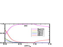
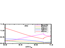
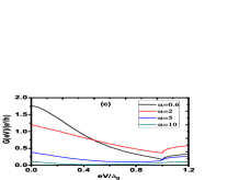
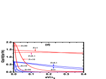
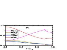
Fig.5(a) shows that when the chemical potentials are not mismatch between the normal lead and the heterostructure superconductor and the magnetic field is absent, there exists a sharp peak corresponding to a resonant spin-reversed Andreev reflection at the induced-gap boundary, similar to the junction G. E. Blonder . A fact that needs to notice is, in the absence of magnetic field, there are no spin-reversed normal reflection and equal-spin Andreev reflection even with strong spin-orbit coupling. This indicates that the magnetic field is a necessity to induce the equal-spin pairing. As shown in Fig.5(b), increasing the magnetic field will drive the peak toward to left (zero-bias voltage) and the finite magnetic field also drives the peak away from the induced-gap boundary. However, when there is a big mismatch between the chemicals, which is usually needed to guarantee that the magnetic filed satisfying the topological criterion is still not large enough to break down the superconductivity, such an interesting phenomenon is absent (no finite-bias peak appears in Fig.3(c)(d)). Once the magnetic field reaches the critical value , a zero-bias conductance peak is formed, however, with the height reduced a lot, as shown in Fig.5(c). A sudden reduction of the peak height maybe imply the zero-bias conductance peak and the finite-bias peak are due to different origins. For weak or intermediate spin-orbit coupling, further increasing the magnetic field has little effect on the zero-bias conductance peak, however, when the spin-orbit coupling is strong enough, the peak height monotonically increases to a parameter-dependent saturation value with increasing magnetic field (here we do not consider the breakdown of superconductivity due to a strong magnetic field), as shown in Fig.5(d). A further study in the stronger spin-orbit coupling region shows that the absence of chemical potential mismatch makes the zero-bias conductance peak approaching to the quantized value even more difficult.
To discuss the effects of the pairing potential to the tunneling potential, here we adopt the experimental parameters: , eV, meV, V. Mourik , and we choose meV. Fig.6(a) shows the tunneling spectroscopy at zero-temperature. Compared the zero-bias conductance peak with the experiments measured value , here the result should still be several times larger even we consider the temperature’s smearing effect. However, as discussed before, decreasing spin-orbit coupling (intermediate region) has great reduction effect to the peak height. In Fig.6(b), it is shown halving the spin-orbit coupling almost corresponds to halving the peak height. Therefore, if the spin-orbit coupling is several times smaller than the reported one, the height of the zero-bias conductance peak will decrease to be comparable with the experiments measured value. Fig.6(b) also shows that decreasing the pairing potential, the peak height is greatly increased. For sufficient small pairing potential, the zero-bias conductance peak is found almost quantized. This result seems counterintuitive, as the pairing potential is a necessity to induce the topological superconductor. This confusion can be clarified by the fact that when , the upper band’s effect is negligible, as a result, the system is an “effective -wave” superconductor J. Alicea1 . This suggests to observe a more striking peak in experiments, it is better to choose a relative weaker pairing potential proximity superconductor.
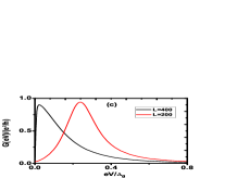
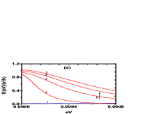
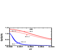
The effects of finite length for junction is similar to the junction, that is, a conductance peak will locate at finite-bias voltage when is not sufficiently long, and with the increase of , the peak moves toward to the zero-bias voltage, see Fig.6(c). For sufficiently long wire, we find that, increasing the magnetic field, the width of the zero-bias conductance peak will be greatly widened, see Fig.6(d).
III Discussion and conclusion
In this work, based on the BTK method, we give a thorough study of the tunneling spectroscopy of junction and junction. Comparing the tunneling spectroscopy of junction with junction’s, we find zero-bias conductance peak appears in both systems when their topological criterions are satisfied, respectively. However, contrary to the stable quantized zero-bias peak of the junction, the zero-bias conductance peak of the junction is non-quantized and sensitive to parameters. The non-quantization of the zero-bias conductance peak does not mean the Majorana end state is absent, its existence is guaranteed by the nontrivial topology of the bulk and the bulk-edge correspondence Y. Hatsugai . The non-quantization only indicates that there are more transport channels compared to the junction. For small and intermediate spin-orbit coupling, we find the additional channels have important contributions to the transport. This indicates the perfect equal-spin Andreev reflection is absent, and the heterostructure superconductor always has a considerable gap to a truly -wave superconductor. And therefore, even the topological criterion is satisfied, using a Majorana chain to denote the heterostructure superconductor and then based on the “interface electron-Majorana hopping” model K. T. Law ; Karsten Flensberg , expecting a quantized zero-bias conductance peak to emerge, is usually unjustified.
For strong spin-orbit coupling, we find that although, for weak interface scattering potential, the zero-bias conductance peak is very small and monotonically decreasing with increasing spin-orbit coupling, a very strong interface scattering potential can suppress the additional transport channels effectively and make the equal-spin Andreev reflection get very close to the perfect level, with the zero-bias conductance peak approaching the quantized value. However, a strong spin-orbit coupling is hard to realize, and a very strong interface scattering potential also makes the width of the zero-bias conductance peak very narrow, which will make detection difficult. Contrary to a combination of strong spin-orbit coupling and strong interface scattering potential, decreasing the pairing potential is a much more effective way to suppress the additional channels and enhance the zero-bias conductance peak to the quantized value.
Besides a zero-bias peak appearing when the system is driven into the topological phase, there are another two common features appearing in the figures. The first one is when the system goes from the normal phase to the topological phase, the equal-spin Andreev reflection amplitude at the neighborhood of zero-bias voltage always has a sudden and comparatively large increment. This indicates that in the topological region, the equal-spin pairing becomes important, and the zero-bias conductance peak must be related to the equal-spin pairing at zero-bias voltage. From Fig.12, we also see, the larger is, the higher the peak is. A quantized zero-bias conductance peak always corresponds to a perfect equal-spin Andreev reflection, , . This correspondence indicates that can be used as a measure of the “effective”. A larger implies the equal-spin pairing becomes more favored, and this indicates the heterostructure turns to be a more “effective -wave superconductor”. The second one is when the magnetic field is turned on, the discontinuity of the tunneling spectroscopy at induced-gap boundary is greatly softened. Such a “soft effect” will make the position of the induced-gap boundary hard to detect, and as a result, the gap closure is also hard to detect. Therefore, the “soft effect” induced by magnetic field can be supplied as a possible explanation of the missing observation of the gap closure. Soft gap induced by other reasons was discussed in detail in Ref.So Takei .
In conclusion, adopting the experimental parameters, we compare the tunneling spectroscopy obtained with the experiment and find that, even without consideration of effects due to disorder, subbands and other inhomogeneities, the observation of a non-quantized value under the experimental parameters is a natural result. And furthermore, a spin-orbit coupling several times smaller than the reported one in experiment, which can be taken as a possible explanation of the quite small zero-bias conductance observed in experiments. We suggest that, to observe a more striking zero-bias conductance peak in future experiments, a weaker pairing potential proximity superconductor is probably a better choice.
Acknowledgments
This work is supported by NSFC. Grant No.11275180.
Appendix: Quantized zero-bias conductance peak of the junction
For junction, the velocity operator and are given as (),
| (41) | |||||
| (46) |
For , the wave function in the -wave superconductor (here we consider the length is infinity) takes a simpler form,
| (51) |
where . The wave function in the normal lead takes the form
| (56) |
here , and we use to denote both of them. By matching the two wave function according to the boundary conditions (19), we obtain
| (57) |
A direct calculation gives
| (58) |
indicates no normal reflection and indicates a perfect equal-spin Andreev reflection. According to the formula (20), the differential tunneling conductance at is
| (59) | |||||
the zero-bias conductance is quantized and independent of the interface scattering potential.
References
- (1) D. A. Ivanov, Phys. Rev. Lett. 86, 268 (2001).
- (2) A. Yu. Kitaev, Ann Phys. 303, 2 (2003).
- (3) S. Das Sarma, M. Freedman, and C. Nayak, Phys. Rev. Lett. 94, 166802 (2005).
- (4) C. Nayak, S. H. Simon, A. Stern, M. Freedman, and S. Das Sarma, Rev. Mod. Phys. 80, 1083 (2008).
- (5) N. Read and D. Green, Phys. Rev. B 61, 10267 (2000).
- (6) A. Yu. Kitaev, Phys.-Usp. 44, 131 (2001).
- (7) A. P. Mackenzie and Y. Maeno, Rev. Mod. Phys. 75, 657 (2003).
- (8) C. Kallian, Rep. Prog. Phys. 75, 042501 (2012).
- (9) Liang Fu and C. Kane, Phys. Rev. Lett. 100, 096407 (2008).
- (10) Jay D. Sau, Roman M. Lutchyn, Sumanta Tewari, and S. Das Sarma, Phys. Rev. Lett. 104, 040502 (2010).
- (11) Roman M. Lutchyn, Jay D. Sau, and S. Das Sarma, Phys. Rev. Lett. 105, 077001 (2010).
- (12) Y. Oreg, G. Refael, and F. von. Oppen, Phys. Rev. Lett. 105, 177002 (2010).
- (13) J. Alicea, Phys. Rev. B 81, 125318 (2010).
- (14) A. C. Potter and P. A. Lee, Phys. Rev. Lett. 105, 227003 (2010).
- (15) J. Alicea, Rep. Prog. Phys. 75 076501 (2012).
- (16) T. D. Stanescu and S. Tewari, J. Phys.: Condens. Matter 25, 233201 (2013).
- (17) K. Sengupta, I. uti, H. J. Kwon, V. M. Yakovenko, and S. Das Sarma, Phys.Rev. B 63, 144531 (2001).
- (18) C. J. Bolech, and Eugene Demler, Phy. Rev. Lett. 98, 237002 (2007).
- (19) Johan Nilsson, A. R. Akhmerov, and C. W. J. Beenakker, Phys. Rev. Lett. 101, 120403 (2008).
- (20) Liang Fu and C. L. Kane, Phys. Rev. Lett. 102, 216403 (2009).
- (21) A. R. Akhmerov, Johan Nilsson, and C. W. J. Beenakker, Phys. Rev. Lett. 102, 216404 (2009).
- (22) K. T. Law, Patrick A. Lee, and T. K. Ng, Phys. Rev. Lett. 103, 237001 (2009).
- (23) K. Flensberg, Phys. Rev. B 82, 180516(R) (2010).
- (24) Stefan Walter, Thomas L. Schmidt, Kjetil Børkje, and Bjorn Trauzette, Phys. Rev. B 84, 224510 (2011).
- (25) Dong E. Liu and Harold U. Baranger, Phys. Rev. B 84, 201308(R) (2011).
- (26) A. R. Akhmerov, J. P. Dahlhaus, F. Hassler, M. Wimmer, and C. W. J. Beenakker, Phys. Rev. Lett. 106, 057001 (2011).
- (27) Rok Žitko, Phys. Rev. B 83, 195137 (2011).
- (28) Yunshan Cao, Peiyue Wang, Gang Xiong, Ming Gong, and Xin-Qi Li, Phys. Rev. B 86, 115311 (2012).
- (29) Shuo Mi, D. I. Pikulin, M. Wimmer, and C. W. J. Beenakker, Phys. Rev. B 87, 241405(R) (2013).
- (30) Zhi Wang, Xue-Yuan Hu, Qi-Feng Liang, and Xiao Hu, Phys. Rev. B 87, 214513 (2013).
- (31) P. A. Ioselevich and M. V. Feigel man, Phys. Rev. Lett. 106, 077003 (2011).
- (32) L. Jiang, D. Pekker, J. Alicea, G. Refael, Y. Oreg, and F. von Oppen, Phys. Rev. Lett. 107, 236401 (2011).
- (33) Pablo San-Jose, Elsa Prada, and Ramó n Aguado, Phys. Rev. Lett. 108, 257001 (2012).
- (34) Fernando Domínguez, Fabian Hassler, and Gloria Platero, Phys. Rev. B 86, 140503(R) (2012).
- (35) L. Jiang, D. Pekker, J. Alicea, G. Refael, Y. Oreg, A. Brataas, and F. von Oppen, Phys. Rev. B 87, 075438 (2013).
- (36) Colin Benjamin and Jiannis K. Pachos, Phys. Rev. B 81, 085101 (2010).
- (37) Chao-Xing Liu and Bjorn Trauzette, Phys. Rev. B 83, 220510(R) (2011).
- (38) Andrej Mesaros, Stefanos Papanikolaou, and Jan Zaanen, Phys. Rev. B 84, 041409(R) (2011).
- (39) V. Mourik, K. Zou, S. R. Plissard, E. P. A. M. Bakkers, and L. P. Kouwenhoven, Science 336, 1003 (2012).
- (40) A. Das, Y. Ronen, Y. Most, Y. Oreg, M. Heiblum, and H. Shtrikman, Nat.Phys. 8, 887 (2012).
- (41) M. T. Deng, C. L. Yu, G. Y. Huang, M. Larson, P. Caroff, and H. Q. Xu, Nano Lett. 12, 6414 (2012).
- (42) A. D. K. Finck, D. J. Van Harlingen, P. K. Mohseni, K. Jung, and X. Li, Phys. Rev. Lett. 110, 126406 (2013).
- (43) E. Prada, P. San-Jose, and R. Aguado, Phys. Rev. B 86, 180503(R) (2012).
- (44) Tudor D. Stanescu, Sumanta Tewari, Jay D. Sau, and S. Das Sarma, Phys. Rev. Lett. 109, 266402 (2012).
- (45) C.-H. Lin, J. D. Sau, and S. Das Sarma, Phys. Rev. B 86, 224511 (2012).
- (46) E. J. H. Lee, X. Jiang, R. Aguado, G. Katsaros, C. M. Lieber, and S. De Franceschi, Phys. Rev. Lett. 109, 186802 (2012).
- (47) G. Kells, D. Meidan, and P. W. Brouwer, Phys. Rev. B 86, 100503(R) (2012).
- (48) J. Liu, A. C. Potter, K. T. Law, and P. A. Lee, Phys. Rev. Lett. 109, 267002 (2012).
- (49) D. Bagrets and A. Altland, Phys. Rev. Lett. 109, 227005 (2012).
- (50) D. I. Pikulin, J. P. Dahlhaus, M. Wimmer, H. Schomerus, and C. W. J. Beenakker, New J. Phys. 14, 125011 (2012).
- (51) D. Rainis, L. Trifunovic, J. Klinovaja, and D. Loss, Phys. Rev. B 87, 024515 (2013).
- (52) D. Roy, N. Bondyopadhaya, and S. Tewari, Phys. Rev. B 88, 020502(R) (2013).
- (53) G. E. Blonder, M. Tinkham, and T. M. Klapwijk, Phys. Rev. B 25, 4515 (1982).
- (54) L. W. Molenkamp, G. Schmidt, and G. E. W. Bauer, Phys. Rev. B 64, 121202(R) (2001).
- (55) Y. Hatsugai, Phys. Rev. Lett. 71, 3697 (1993).
- (56) S. Takei, B. M. Fregoso, H. Y. Hui, A. M. Lobos, and S. Das Sarma, Phys. Rev. Lett. 110, 186803 (2013).