Magnetic domain-wall motion study under an electric field in a Finemet® thin film on flexible substrate
Abstract
Influence of applied in-plane elastic strains on the static magnetic configuration of a 530 nm magnetostrictive FeCuNbSiB (Finemet®) thin film. The in-plane strains are induced via the application of a voltage to a piezoelectric actuator on which the film/substrate system was glued. A quantitative characterization of the voltage dependence of the induced-strain at the surface of the film was performed using a digital image correlation technique. MFM images at remanence ( Oe and V) clearly reveal the presence of weak stripe domains. The effect of the voltage-induced strain shows the existence of a threshold value above, which the break of the stripe configuration set in. For a maximum strain of we succeed in destabilizing the stripes configuration helping the setting up of a complete homogeneous magnetic pattern.
I Introduction
During the last decades technological progress has been driven predominantly by the modern information and communication technology. The steadily increasing data output and functionality of devices has required an ongoing miniaturization of their structural elements. In the design and manufacturing of actual microelectronic and microelectromechanical systems (MEMS), thin metallic films play an important role Niarchos2003 ; Craighead2000 . Thin films can show continuous geometry for which lateral dimensions are much higher than thickness (typically less than one micron), or show complex geometry (wires or dots arrays) for which one or two lateral dimensions and thickness are of same order. Usually, thin films are deposited on substrates, which are several ten times thicker. In the case of flexible substrates (generally polymers) used in stretchable electronics, the thin films are usually submitted to mechanical stresses due to the curvature of the whole system. Obviously, these stresses may have an important effect on the magnetic properties, especially on the effective magnetic anisotropy Dai2012 ; Shin2012 . Magnetic devices fabricated on compliant substrates such as polymers are believed to have great potential for applications due to their mechanical flexibility, enhanced durability and lightweight compared with those on a rigid substrate. Moreover, it has been found that the specific nature of polymer substrates has non-negligible consequence on the magnetic properties of deposited films, which leads to a different performance from a film deposited on rigid substrate. Due to their stress sensitivity, the magnetic properties of magnetostrictive films on flexible substrate can be tailored by the stress Xu2010 ; Ludwig2002 ; Ozkaya2008 ; Iakubov2012 ; Uhrmann2006 . In this context, a few dedicated techniques have been developed to study the magnetelastic behavior of thin films. Concerning magnetic films deposited on flexible substrates, recent papers have reported in situ characterizations by FerroMagnetic Resonance (FMR) Zighem2013 , Magneto-Optical Kerr EffectOzkaya2008 and Giant MagnetoResistance (GMR) measurements Uhrmann2006 ; Barraud2010 ; Melzer2011 . The purpose of these studies is especially to demonstrate the feasibility of a magnetostrictive sensor on a polymer substrate. The main advantage of polymer materials is obviously their high flexibility, which cannot be achieved by crystalline materials, and their relative low cost.
In the present paper, the influence of an applied elastic strain on the magnetic domain of a Finemet® film/Kapton® substrate is investigated. The external loading is applied thanks to a piezoactuator Pi_actuator on which our system is glued, as already shown in previous studies Zighem2013 ; Brandlmaier2009 ; Brandlmaier 2008 . A quantitative study of the voltage-induced elastic in-plane strains is performed thanks to a Digital Image Correlation (DIC) technique while the evolution of magnetic domain structures is probed by Magnetic Force Microscopy (MFM).

II Experimental
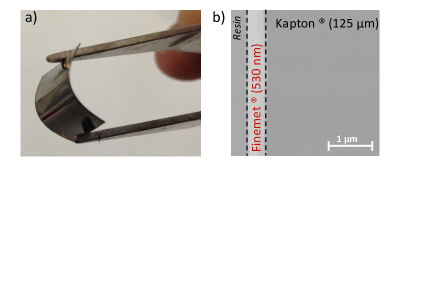
The amorphous Finemet® film has been deposited on Kapton® substrate (125 µm) (shown on figure 1-a) by RF sputtering with the following conditions : residual pressure in the range of 10-7 mbar, working Ar pressure 40 mbar and RF power 250 W. A thin film of titanium was deposited under the layer in order to increase adhesion to the Kapton and over the layer in order to protect from oxidation. The composition of the target was Fe73.5Cu1Nb3Si15.5B7. The film composition has been characterized by EDS and is close to the one of the target. The film thickness (530 nm) has been estimated by Scanning Electron Microscopy equipped with a Field Electron Gun (SEM-FEG) (see the cross-section view on figure 1-b).

After deposition, the flexible film/substrate system was glued onto a piezoelectric actuator. Zighem et al. Zighem2013 have already shown that a compliant substrate allows to have a nearly strain transmission in between the piezoelectric actuator and the film. In the present work, a quantitative characterization of the voltage dependence of the induced-strain at the surface of the film was performed using Digital Image Correlation technique Haddadi2012 . Magnetic Force microscopy (MFM) measurements are performed by using a standard Veeco D3100 microscope. In order to provide reasonables sensitivity and resolution, standard hard magnetic tip (PPP-MFMR tips) are used. The hard magnetic coating of this tip has approximately 300 Oe coercivity and a 300 emu.cm-3 remanence magnetization which allow high magnetic contrast. This latter characteristic is mandatory for weak magnetic stray field detection and high lateral resolution domain imaging (i.e. around 50 nm). The MFM has been used as an in situ probe of the static magnetic domains configuration under the influence of applied in-plane elastic strains. Before this, in order to fully characterize the ferromagnetic film, the ground state ( V) of the system is characterized. We performed standard contact Atomic Force Microscopy (AFM) for a roughness check of the surface of the ferromagnetic film and static magnetization measurements at room temperature for static magnetic behavior.
III Results and discussion
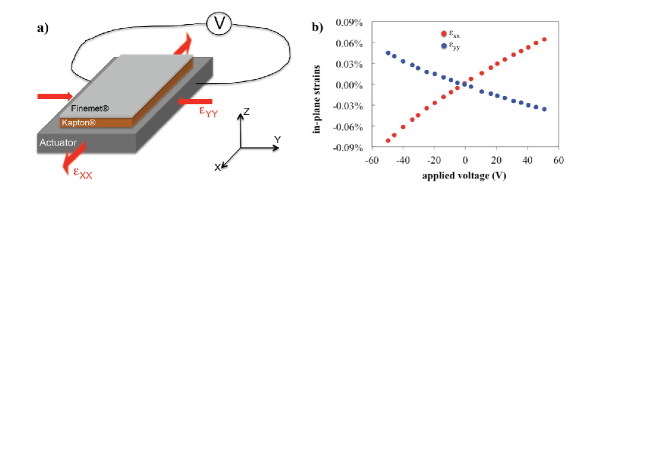
The sketch of the studied artificial multiferroic system made by the 530 nm Finemet® ferromagnetic film deposited onto the compliant polyimide substrate (Kapton®) glued on a piezoelectric device is shown in figure 2-a. This latter allows, via the application of a voltage, to induce in-plane strains ( and ) to the film/substrate, thanks to the choice of the Kapton® substrate which avoids clamping effects leading to low transmission of strains from the actuator to the film/substrate system Brandlmaier 2008 . The DIC measurements have been performed by varying the external voltage from +50 V to -50 V. The measured in-plane strains ( and ) in this range of voltages are presented in Figure 2-b. The reference image for the determination of the in-plane strains has been taken at V (after applying a voltage of V in order to avoid hysteresis effects due to the piezoelectric material). In these conditions, a maximum (resp. minimum) value of 0.065% (resp. -0.035%) for (resp. for ) is found at V. One can note that the values obtained at V are slightly higher (-0.085% for and 0.045 for ) than the ones obtained at V. This behavior is due to the non-linear and hysteretic behavior of the piezoelectric actuator. However, we have verified that no variations of these values are observed after several V to V sweeps (note that the sweep V to V is not shown here). In addition, one can note that the sketch presented in figure 2-a corresponds to a positive applied voltage where the magnetic film is tensily stressed (when a negative voltage is applied, the film is compressively stressed).
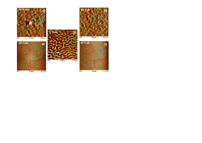
The influence of voltage-induced in-plane elastic strains on the magnetic domain of the film has been probed by MFM. The presence of magnetic domains has been clearly identified at zero applied voltage by MFM (see figure 3-a). This kind of micromagnetic configuration appears in magnetic film presenting an out-of plane magnetic anisotropy (uniaxial in the present case) under specific conditions. Indeed, the magnetic domains presented in figure 3-a appear only if the thickness of the film is higher than a critical thickness where is the exchange stiffness and is the out-of-plane magnetic anisotropy constant and if is smaller than the demagnetizing energy contribution (here ) Talbi2010 . The thickness of the studied film is around 530 nm which is higher than the calculated critical thickness.
The MFM tip was magnetized along its axis using an external magnet with field kOe in order to have a magnetic moment directed along the apex-base axis of the pyramidal nanometric tip. This moment is a sensitive in situ probe of the stray field coming from the surface of the studied film and always perpendicular to it. As a simple approximation, one can consider a dipole-dipole interaction between the tip and the stray field coming from changes in the micromagnetic configuration of the film. Operating in tapping mode in air, it is easy to find a direct connection between the shift in phase of the eigen resonance frequency of the tip and the force gradient of the dipole-dipole interaction:
In this latter expression is the cantilever spring constant and is the vibrating system quality factor. In these conditions, attractive (resp. repulsive) forces with a positive (resp. negative) gradient lead to a negative (positive) phase-lag: dark contrast (resp. white contrast).


Figure 3 shows the images representation of this phase changes over the observed film surface for different voltage-induced in-plane strains. Tapping voltage set point, drive amplitude of the tip and lift scan distance has been adjusted all along measurements in order to optimize contrast in the phase image variations and to prevent unwanted local magnetization effect of the magnetic film by the MFM tip. Also lift scan distance has been optimized in order to avoid tip demagnetization effect by the stray field of the film. Typical set point values were between 0 and 1.5 Volt and lift distances in the range of 80 to 150 nm. Typical scan area was of µm2 at a scan rate between 0.3 and 0.5 Hz. Both topography and magnetic images were obtained for each strained configuration. In first approximation, black and white regions represent opposite magnetization direction giving place to opposite sign of the dipole-dipole interaction between the tip and the stray field coming from the surface sample. The use and fabrication of the studied heterostructure allows the application of relatively high in-plane strains which lead to drastic change of the micromagnetic configuration inside the film: from “stripe”-domains (see Figure 3-a) to a maze-like pattern (see Figures 3-b and 3-d) and finally to a “macrospin” configuration where no magnetic contrast is observed (see Figures 3-c and 3-e). Specifically, Figure 3b-d show that the domain structure is transformed into a maze-like complex pattern all over the studied surface when a voltage of V and V is applied.
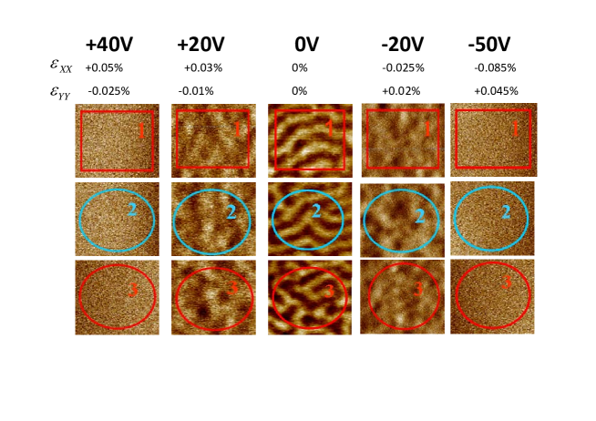
These changes are due to the voltage-induced strain control of the magnetoelastic anisotropy of the Finemet® film. In first approximation, this magnetoelastic anisotropy contribution can be view as a static magnetic field applied in the plane of the film. It should noted that very small induced strains are sufficient to modify the micromagnetic configurations into an apparent uniform configuration. This extreme sensivity of the magnetic configuration is due to the non-negligible magnetostriction of the studied film. In order to strengthen these observations, we show here in Figures 4 a zoom-in of specific boxed regions in figures 3 (box 1, 2 and 3). It is clear from all the three zones chosen (i.e. bended+curved domains=zone 1, stripe parallel domains=zone 2 and puzzled-like domains=zone 3) that after the application of +20 V strains big displacement of domain-walls happened letting a different maze-like pattern to set in. At -20 V, this latter presents the same main features but with opposite magnetic domain orientations (i.e. white and black domains are exchanged). After the application of +40 V exactly as for -50 V (see Figures 3 and 4) the domain pattern is fully supressed and an apparent uniform magnetic configuration set in. In this latter phase images, the slight change in colors have to be ascribed to the sample roughness, which can locally influence the magnetic stray field.
IV Conclusions
In conclusion we investigated the influence of an applied elastic strain on the magnetic domain of a Finemet® film/Kapton® substrate. The applied elastic strains were controlled by applying voltage to a piezo-actuator on which the Finemet®/Kapton® where glued. The amount of strains was measured by Digital Image Correlation while using Magnetic Force Microscopy (MFM) we probed changes in magnetic domain structures. MFM images at remanence (H=0Oe and U=0V) clearly reveal the presence of weak stripe domains. We have found that magnetic domains in Finemet® alloy films showed high mobility upon small applied strains. A threshold value of the electric field applied has been observed. Above this latter the break of the stripe configuration sets in by bending, curving and branching of domains and gives way to a maze-like configuration. For a maximum strain of the stripes configuration is destabilized and a complete homogeneous magnetic pattern appeared.
V Acknowledgments
The authors gratefully acknowledge the CNRS for their financial support in the framework of the “PEPS INSIS” program (“Ferroflex” project). Ngo Thi Lan is grateful to the Labex SEAM for her financial support during her stay in Paris 13th University. This work was also partially supported by the French Research Agency (project ANR 2010 JCJC 090601 entitled “SpinStress”).
References
- (1) D. Niarchos, Sensors and Actuators A 109, 166 (2003)
- (2) H. G. Craighead, Science 290, 1532 (2000)
- (3) G. Dai, Q. Zhang, Y. Liu, H. Yang, X. Zhang, B. Chen, R.-W. Li, Appl. Phys. Letters 100, 122407 (2012)
- (4) J. Shin, S. H. Kim, Y. Suwa, S. Hashi, K. Ishiyama, J. Appl. Physics 111, 07E511 (2012)
- (5) F. Xu, X. Chen, N.N. Phuoc, X.Y. Zhang, Y.G. Ma, C.K. Ong, J. Magn. Magn. Mater. 322, 3262 (2010)
- (6) M.T.A. Ludwig, S. Glasmachers, M. Lohndorf, E. Quandt, J. Magn. Magn. Mater. 242, 1126 (2002)
- (7) B. Ozkaya, S.R. Saranu, S. Mohanan, U. Herr, Physica Status Solidi (a), 205, 1876 (2008)
- (8) I. T. Iakubov, O. Y. Kashurkin, A. N. Lagarkov, S. A. Maklakov, A. V. Osipov, K. N. Rozanov, I. A. Ryzhikov, S. N. Starostenko, J. Mag. Mag. Mater. 324, 3385 (2012)
- (9) T. Uhrmann, L. Bär, T. Dimopoulos, N. Wiese, M. Rührig, A. Lechner, J. Magn. Magn. Mater. 307, 209 (2006)
- (10) F. Zighem, D. Faurie, S. Mercone, M. Belmeguenai, H. Haddadi, J. Appl. Phys. 114, 073902 (2013)
- (11) C. Barraud, C. Deranlot, P. Seneor, R. Mattana, B. Dlubak, S. Fusil, K. Bouzehouane, D; Deneuve, F. Petroff, A. Fert, Appl. Phys. Letters 96, 072502 (2010)
- (12) M. Melzer, D. Makarov, A. Calvimontes, D. Karnaushenko, S. Baunack, R. Kaltofen, Y. Mei, O. G. Schmidt, Nano Lett. 11, 2522 (2011)
- (13) http://www.physikinstrumente.com/
- (14) M. Weiler, A. Brandlmaier, S. Geprägs, M. Althammer, M. Opel, C. Bihler, H. Huebl, M. S. Brandt, R. Grossand S. T. B. Goennenwein, New Journal of Physics 11, 013021 (2009)
- (15) A. Brandlmaier, S. Geprägs, M. Weiler, A. Boger, M. Opel, H. Huebl, C. Bihler, M. S. Brandt, R. Gross and S. T. B. Goennenwein, Phys. Rev. B 77, 104445 (2008)
- (16) H. Haddadi and S. Belhabib, Int. J. of Mech. Sc. 62, 47 (2012)
- (17) Y. Talbi, Y. Roussigné, P. Djemia and M. Labrune, Journal of Physics: Conference Series 200 042027 (2010)