Using Topological Insulator Proximity to Generate Perfectly Conducting Channels
in Materials without Topological Protection
Abstract
We show that hybrid structures of topological insulators and materials without topological protection can be employed to create perfectly conducting channels hosted in the non-topological part. These states inherit the topological protection from the proximity of the topological insulator but are more fragile to time-reversal symmetry breaking because of their extended character. We explore their formation in the band structure of model hybrid systems as well as realistic heterostructures involving HgTe/CdTe-based two-dimensional topological insulators. Using numerical quantum transport calculations for the HgTe/CdTe material system we propose two experimental settings which allow for the detection of the induced perfectly conducting channels, both in the localized and diffusive regime, by means of magneto conductance and shot noise.
pacs:
72.10.-d, 73.20.At, 73.21.AcOne important feature of the topological classification of insulators Schnyder2008 is the existence of gapless states at interfaces between materials which differ in their topological quantum number. In this way, one can understand the formation of quasi one-dimensional (1d) edge channels in quantum Hall systems and in two-dimensional (2d) topological insulators (TI) at the interface between the topologically non-trivial insulator and the trivial insulating vacuum. These edge channels carry the unique property of being perfectly conducting, even in presence of impurity scattering, corresponding to transmission eigenvalues of one. Such quantized, spin-polarized channels along the boundaries of a 2d TI crystal have already been detected experimentally Brune2012 and give rise to peculiar conductance phenomena such as the quantum spin Hall effect V_Bernevig2006 ; Konig2007 .
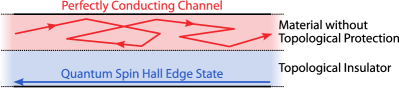
In this paper we show that perfectly conducting channels (PCCs) can be induced in materials without topological protection by the proximity of a 2d TI as sketched in Fig. 1. In such a hybrid structure the non-topological material could be a (disordered) metal, a gated semi-conductor or even a conventional Anderson insulator. Such a setup exploits the hybridization of the upper TI edge state with the bulk states of the normal material, leading to an imbalance of left and right moving states in the normal material and thereby to a PCC therein note1. The emergence of PCCs in isolated non-topological systems has been earlier predicted for carbon nanotubes V_Ando2002 and graphene nanoribbons V_Wakabayashi2007 ; V_Wurm2012 . There the PCC was shown V_Wakabayashi2007 to arise from an uneven separation of left and right moving states associated with specific (valley) symmetries V_Wurm2012 . However, since atomic defects or short-ranged impurity potentials break this symmetry, PCCs are rather fragile in these graphene-based systems and have not yet been observed therein. Contrarily, the proximity-induced PCCs reported here are robust against any kind of disorder as long as time-reversal symmetry is preserved, even in presence of spin-orbit coupling.
To our knowledge this phenomenon has not been discussed before in 2d heterostructures, only layers made of 2d TIs nested in 3d systems Hutasoit2011 ; Wang2013 ; Yang2013 and pure insulator heterostructures xiao2013proximity have been considered very recently.
In the following, we first demonstrate the emergence of a proximity-induced PCC by means of a band structure analysis within a simplified model calculation. Subsequently, we will present numerical results that show the same features in HgTe/CdTe-based ribbons. Furthermore, we will study features of the PCC in quantum transport for experimentally realizable setups. In particular we reveal the creation of a PCC in an otherwise insulating disordered strip and how to disentangle the signature of a PCC from the diffusive modes in a disordered conductor.
Throughout this manuscript we model the electronic structure of a 2d HgTe/CdTe quantum-well by the four-band Bernevig-Hughes-Zhang (BHZ) Hamiltonian V_Bernevig2006 ,
| (1) |
with spin-subblock Hamiltonians
| (2) |
where and . In Eq. (1), the off-diagonal coupling parameter describes a Dresselhaus-type spin-orbit coupling of the two spin blocks Rothe2010 .
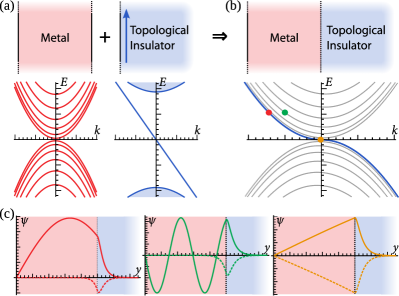
We consider a 2d heterostructure of a usual conductor and a semi-infinite topological insulator plane. It is instructive to first look at a simplified model system which already captures the important physical features. The metal part note2 is modeled by the Hamiltonian (1) with , describing a free electron-hole gas. Confined to a finite-width strip by hard wall boundary conditions, this leads to an electron-hole symmetric parabolic band structure, as shown in Fig. 2(a). For the TI half plane, we use a minimal BHZ Hamiltonian (), which splits up into two electron-hole symmetric spin blocks. The band structure for one spin block shown in Fig. 2(a) exhibits the bulk band gap and a single edge state. A coupling between the two systems is implemented by replacing the central hard wall constraint by the continuity of the wave function and the flux across the interface. The resulting band structure, shown in Fig. 2(b), resembles the one of the metallic strip, but contains an extra band (marked in blue) as a remainder of the topological edge state, which does not feature the linear momentum dependence because of band repulsion due to hybridization. The wave functions at various energies in Fig. 2(c) reveal that all states are predominantly localized in the metallic region and only small exponential tails remain in the TI part. Thus, we do not find evidence for an induced non-trivial topology as reported in Ref. xiao2013proximity, , from which one would expect a new interface state forming on the outer hard wall boundary. Instead, the former edge state fully hybridizes with the metallic bands and covers the whole extended state region! This is in line with Ref. Wang2013, where the authors also observe an extended metallic state in a 3d heterostructure, but differs from the findings of Ref. Yang2013, , where a protection from hybridization for topological edge states is reported for a 2d quantum Hall insulator on top of a 3d substrate.
The above result has important consequences. Counting the bands in Fig. 2(b) reveals an imbalance between left and right movers (up and down movers in Fig. 2), which leads to a PCC at any Fermi energy. Including the other spin block and spin-orbit interaction only slightly changes this picture. Since both spin blocks feature a PCC with opposite propagation direction in the decoupled system, the combined system has an equal but odd number of left and right moving channels. Due to the time-reversal symmetry of the Hamiltonian, the scattering matrix can be written in a basis where it is anti-symmetric. Together with the odd number of channels, this implies a single PCC in each direction Bardarson2008 . As the wave functions of all channels are predominantly localized in the metallic region, one can say that the proximity of the TI induces a single additional channel in each direction leading to one net PCC in the metallic region. In other words, the quasi 1d edge state of the TI migrates into the metallic region and forms an extended PCC. We believe that this is generally true for materials with extended states. It should provide a valuable tool to create and observe PCCs as they inherit the topological protection of the former edge channels and are expected to be stable for any disorder and interface type, as long as the latter allows for sufficient hybridization.
Given that the TI is a good insulator, i.e., that the decay length of the states inside the insulator is short compared to the width of the metallic ribbon, one expects that only a vanishing part of the probability density of a state is inside the TI. This allows for replacing the explicit consideration of the TI by an effective boundary condition for the wave function inside the metallic ribbon. For the right boundary of a heterostructure in -direction it reads:
| (3) | |||||
| (4) |
where denotes the -th component of the state obtained by applying the velocity operator normal to the boundary. Note that, Eq. (53) still contain a free parameter , which stems from the band curvature of the TI. The effect is best seen by applying the boundary conditions to a topologically trivial insulator, like a gapped electron-hole gas: Then the group velocity of the emergent edge state band linearly depends on . Using the boundary conditions on the gapless electron-hole gas from the previous model heterostructure, Fig. 2(a), we obtain for qualitatively the same band structure as in Fig. 2(b). While Eq. (3) is a simple Dirichlet boundary condition that fixes the phase of the two components, Eq. (53) is of the Robin type gustafson1998third , i.e., it links the wave function at the boundary to its derivative. This -dependent mixing induces the PCC in the adjacent metal, as illustrated in the Supplemental Material support .
For the practical observation of a PCC in such heterostructures the semi-infinite TI plane can be replaced by a TI-ribbon in a four-lead geometry, see Fig. 3(a). This geometry decouples the edge channel on the lower edge of the TI from the region with the PCC. This is necessary, as the lower edge state would add another channel to the scattering matrix, make it even dimensional and therefore lift the protection of the PCC. If the PCC in the upper metal is well coupled to the two metallic leads (e.g., by making the leads wide), the total transmission between the upper leads will be at least one. Even in presence of disorder there will be no complete localization independent of the system length.
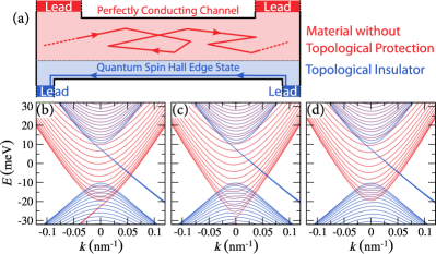
It is not required to assemble the heterostructure presented in Fig. 3(a) from two different materials. For convenience the whole system can consist of a common HgTe/CdTe quantum well with inverted band order, where only the upper (metallic) part has a Fermi energy outside the TI bandgap, a setting that can be realized by local gating. Such a setup leads to a hybridization of the upper pair of edge states of the TI with the bulk states of the metallic part, while the lower pair is still localized at the lower edge of the TI. The corresponding band structure in Fig. 3(b) reveals that a single spin block contains an additional right moving state (red lines), whereas the left mover is still localized at the opposite boundary in the TI region (blue). Furthermore, we stress that an inverted band order is not strictly necessary to induce a PCC. The bands of a gapless metallic strip [see Fig. 3(c)] as well as a strip with conventional ordering [see Fig. 3(d)] also feature an additional right moving state in proximity to a TI. This implies that PCCs can be induced by the same mechanism in other semiconductors if the two materials can be coupled efficiently and the crossover of the band topology takes place in the metallic part or at the interface.
Experimental evidence for the induction of a PCC can be for example accomplished by means of magneto transport measurements in the localized regime. To this end, we suggest a four-terminal configuration based on a 2d-TI like HgTe/CdTe, as sketched in the inset of Fig. 4(a).
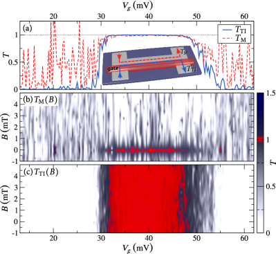
We assume the Fermi energy outside the topological band gap, such that propagating states exist in the bulk of the corresponding clean material. For strong disorder associated with a localization length shorter than the length of the ribbon connecting the left and right terminals, the total transmission between the upper leads and between the lower leads is strongly suppressed. To achieve TI properties in the lower part of the strip, a gate is applied to locally shift the band structure of a region containing the edge and the entire connection between the strip and the lower leads [red region in the inset of Fig. 4(a)]. To illustrate the signatures of the PCC the transport properties of this setup are calculated for different gate potentials by means of a recursive Greens function algorithm Wimmer2009 . If the gated part is tuned such that the Fermi energy is in the TI bandgap, the suppressed transmission of the localized regime takes the quantized value of the quantum spin Hall edge state. This behavior of is shown in Fig. 4(a) by the solid (blue) line for gate voltages between and . Remarkably, the transmission between the two upper leads exhibits the same behavior and gets quantized, although there is no material with topological protection linking the two terminals. This quantized transmission in the otherwise localized regime is a clear-cut signature of and carried by the PCC.
The different nature of the PCC compared to the quantum spin Hall edge state can be probed by a perpendicular magnetic field . Since the PCC state is extended over the entire spatial region of the upper strip, which can be seen in the local density of states support , a weak field generating a flux , where is the flux quantum, is sufficient to effectively break the time-reversal symmetry. The numerical data presented in Fig. 4(b) shows that the conductance quantization of is fully destroyed for a magnetic field of , corresponding to penetrating the device. This is not the case for the robust quantum spin Hall edge state, which is strongly localized at the lower boundary and accordingly quasi one-dimensional. As a result, the magneto transport is insensitive to magnetic fields in the regime, as shown for in Fig. 4(c). As a side remark, the PCC turns out to be completely spin mixed already at small spin-orbit strengths , in contrast to the quantum spin Hall edge channels, which remain spin-polarized up to moderate spin-orbit strengths support .
If the electronic states of the disordered strip are not localized the total transmission also contains contributions of non-perfectly conducting channels.
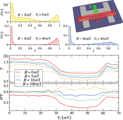
For diffusive transport the distribution of these transmission eigenvalues features a bimodal distribution Dorokhov1984381 ; RevModPhys.69.731 , see upper left panel of Fig. 5(a), whose intermediate transmission eigenvalues mask the PCC when considering . In this case an additional tunnel barrier, depicted by the green bar in the sketch of Fig. 5, can be used to unravel the presence of the PCC. The probability for finding these intermediate transmission eigenvalues can be strongly reduced by the tunnel barrier (parametrized by ), as shown in Fig. 5(a) for , . Hence, for this configuration is mainly carried by the PCC. As in the localized case, protection of the PCC can be broken by a magnetic flux leading to a broader distribution for the high transmission eigenvalues [right panel in Fig. 5(a)].
The change of this probability distribution is also reflected in transport quantities, which can be experimentally probed. For example, upon raising the tunnel barrier the transmission at exhibits a quantized minimum, which reflects the presence of a PCC, as shown by the red line in Fig. 5(b) for . As expected, this feature disappears at small magnetic fields.
A more pronounced PCC signature is found in the shot noise power PhysRevLett.65.2901 , , depending on the transmission eigenvalues between the upper leads. For conventional diffusive transport the bimodal distribution leads to a universal suppression of the shot noise [, as marked by a dashed line in Fig. 5(c)], independent of the universality class of the material PhysRevB.46.1889 . In presence of a tunnel barrier all except the one of the PCC tend to zero, leading to a characteristic shot noise suppression, as shown by our numerics in Fig. 5(c) for . A -field destroys the PCC, which in turn removes the shot noise suppression. At finite , in absence of the PCC the shot noise signal even increases above due to the tunnel barrier. We suggest the tunnel conductance and shot noise as promising, experimentally accessible observables to verify the TI proximity induced PCC.
To summarize, we showed that the proximity of a 2d topological insulator (TI) creates a robust perfectly conducting channel (PCC) in an adjacent non-topological material. We believe this is a quite general effect that should work for almost all materials with extended states. We expect that a similar phenomenon exists for a disordered conductor at the surface of a 3d TI. In addition, we showed that the proximity of a 2d TI to a metal can be understood in terms of a Robin type effective boundary condition, responsible for the creation of the PCC. This does not only allow simplifications in future theoretical studies, but might also pave the way to induce PCCs by artificially creating such boundary conditions, e.g., by using metamaterials for electromagnetic waves, without relying on TI heterostructures.
This work is supported by DFG (SPP 1666 and joined DFG-JST Research Unit FOR 1483). We thank I. Adagideli and M. Wimmer for useful conversations.
References
- (1) A. Schnyder, S. Ryu, A. Furusaki, and A. Ludwig, Phys. Rev. B 78, 195125 (2008).
- (2) C. Brüne et al., Nature Phys. 8, 485 (2012).
- (3) B. A. Bernevig, T. L. Hughes, and S.-C. Zhang, Science 314, 1757 (2006).
- (4) M. König et al., Science 318, 766 (2007).
- (5) Strictly speaking, the argument of channel imbalance only applies if the spin is conserved. However, the PCC also persists in presence of spin-orbit coupling as long as time-reversal symmetry holds, since such a setting leads to an odd number of channels in each direction.
- (6) T. Ando and H. Suzuura, J. Phys. Soc. Jpn. 71, 2753 (2002).
- (7) K. Wakabayashi, Y. Takane, and M. Sigrist, Phys. Rev. Lett. 99, 036601 (2007).
- (8) J. Wurm, M. Wimmer, and K. Richter, Phys. Rev. B 85, 245418 (2012).
- (9) J. A. Hutasoit and T. D. Stanescu, Phys. Rev. B 84, 085103 (2011).
- (10) X. Wang, G. Bian, T. Miller, and T.-C. Chiang, Phys. Rev. B 87, 235113 (2013).
- (11) B.-J. Yang, M. S. Bahramy, and N. Nagaosa, Nature Commun. 4, 1524 (2013).
- (12) L. Xiao-Guang et al., Chin. Phys. B 22, 097306 (2013).
- (13) D. G. Rothe et al., New J. Phys. 12, 065012 (2010).
- (14) We use the term “metal” synonymously to “material with extended states” also referring to a gated semiconductor.
- (15) J. H. Bardarson, J. Phys. A 41, 405203 (2008).
- (16) K. Gustafson and T. Abe, Math. Intell. 20, 63 (1998).
- (17) See Appendix for the derivation of the effective boundary condition and details about the numerical model and spatial densities of the PCC.
- (18) M. Wimmer and K. Richter, J. Comp. Phys. 228, 8548 (2009).
- (19) O. Dorokhov, Solid State Comm. 51, 381 (1984).
- (20) C. W. J. Beenakker, Rev. Mod. Phys. 69, 731 (1997).
- (21) M. Büttiker, Phys. Rev. Lett. 65, 2901 (1990).
- (22) C. W. J. Beenakker and M. Büttiker, Phys. Rev. B 46, 1889 (1992).
- (23) M. Levitin and L. Parnovski, Math. Nachr., 281, 272 (2008).
- (24) M. König et al., J. Phys. Soc. Jpn., 77, 031007111 (2008).
Appendix A Band structure calculations
This section provides some details on the band structure calculations shown in Fig. 2 of the main manuscript. We consider a metallic strip of finite width , which borders vacuum on the one side and is in contact with a semi-infinite 2d-TI plane on the other. In the TI part is given by a simplified 2-band BHZ-model
| (5) |
where in the metallic region is simply taken as a free electron-hole gas ()
| (6) |
For simplicity we assume the value of the parameter to be the same in the two regions. To solve for the transverse wave functions in this geometry, we require that the wave function should vanish at the boundary to vacuum at and that should be continuous across the metal-TI boundary at . We also require the probability current to be continuous across the boundary, i.e.,
| (7) |
We then find the secular equation
| (8) | |||||
| (9) |
which may be solved numerically to yield the band structure. Here,
| (10) | |||||
| (11) |
and are the components of the decaying free solutions in the TI-region,
| (12) |
| (13) | |||||
| (14) |
where . The decay coefficients (which have a negative real part as long as ) are given by
Plots of a typical bandstructure obtained from this model are shown in Fig. 2(b) of the main text together with some sample wavefunctions in Fig. 2(c). They were obtained using .
Appendix B Effective boundary condition
B.1 Derivation
One can increase the level of abstraction and still observe the same physics, by not explicitly considering the semi-infinite 2d TI plane but instead replacing it by an effective boundary condition. This is especially justified if the extent of the evanescent wave component into the 2d-TI is small (), such that the transverse wave function is to a good approximation only located inside the metallic region. As the considered model of the TI involves many parameters, there is no unique way of achieving this infinitely fast decay and hence there will be no unique set of boundary conditions. The limiting procedure presented in the following should be understood as one possible way, which will in the end provide a conceptually simple boundary condition, which will capture all important physical features.
For achieving the infinite decay constants we let , i.e., we will consider a TI with an infinite band gap. In addition, we will have to rescale by choosing with a parameter having the units . If one now considers the limit keeping , one finds for the real parts of the decay constants :
| (15) | |||||
| (16) |
meaning that we indeed expect the wave functions not to extend into the TI. For this limit, one can derive the appropriate boundary conditions that any attached two-band Hamiltonian should fulfill. We start from the continuity of the wave function of the metal region and the probability current across the boundary at ,
| (23) | |||||
| (35) | |||||
for so far unknown constants and . We are now interested in the behavior of the right hand sides for the limit discussed above. However, as
| (36) |
one needs to rescale the constants to obtain a finite value of the wave function at the border to the TI:
| (37) |
This way, we find
| (38) | |||||
| (39) |
from Eq. (23). We can now do the limiting process on the right hand side always keeping fixed, using
| (40) | |||||
| (41) | |||||
| (42) | |||||
| (43) |
where, on the way, we made use of the fact that and . To simplify the writing we introduced the functions and . From this, we can already find the first boundary condition, as now
| (44) | |||||
| (45) | |||||
| (46) |
Note that this is independent of the choice of the parameters and . The second boundary condition which links the currents is, however, more complicated and does depend on the choice of and . It can be simplified by additionally choosing , which will then imply
| (47) |
If we now subtract the two components of Eq. (35),
| (48) | |||||
and again perform the limits,
| (49) | |||||
| (50) |
we obtain
Here, we already made use of the first boundary condition. In total we find, that the boundary to a TI in the limit discussed above can be approximately described by the following boundary conditions, which still contain one free parameter,
| (52) | |||||
| (53) |
which we renamed from to , to distinguish it from the band curvature of the material on which we enforce this boundary condition. Like this we can generalize the case discussed in Sec. B.1 and need not restrict ourselves to heterostructures of materials with the same band curvature.
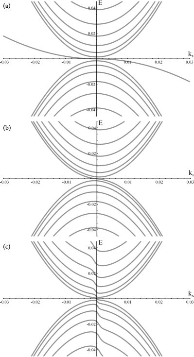
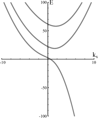
Fig. (6) shows band structure calculations using the boundary conditions with different choices for the parameter . One notes that for one almost recovers the band structure from Fig. 2(b) of the main text which was obtained by a full calculation which explicitly includes the TI half-plane.
In the derivation, we assumed the TI half plane to extend in the positive -direction, which is why we matched the exponentially decaying wave functions on the TI side. Of course the same calculation can in principle be redone for an arbitrary interface orientation. E.g., choosing the TI plane to extend in the negative -direction with a boundary at , leads to the following set of boundary conditions:
| (54) | |||||
| (55) |
i.e., we find an additional phase factor in front of one wave function component.
B.2 Effect of Robin boundary condition
To show that it is indeed the Robin boundary condition, Eq. (53) or (55), which is responsible for the appearance of a perfectly conducting channel, we consider a one-component free electron gas Hamiltonian
| (56) |
subject to hard wall boundary conditions at () and a one-component version of the boundary condition from Eq. (53) at :
| (57) | |||||
| (58) |
For one obtains a band structures similar to the one shown in Fig. 7, which has been calculated by setting . It resembles the simple parabolic band structure that one obtains by putting hard wall (or Neumann) boundary conditions on both sides, but it contains an extra band which tends to negative energies with increasing and thereby creates a PCC. While the emergence of large negative eigenvalues is known for Robin problems with large negative parameters levitin2008principal , as far as we know there has not been a discussion on the emergence of perfecly conducting channels in one-sided Robin wave guides so far.
By implementing this boundary condition, or a similar one (e.g. by replacing in Eq. (58) by a different but still odd function of ), on one side of a wave guide, one should be able to create PCCs for many scenarios, i.e., for quantum as well as electromagnetic wave guides.
Appendix C Transport Calculations
In the manuscript we use numerical quantum transport calculations to investigate the transport signatures of a PCC, which is induced in a conventional metal by the proximity of a TI. To this end, we propose two different setups, which will be introduced in more detail in the following. Both of them are based on a common HgTe/CdTe heterostructure, described by the BHZ Hamiltonian (1) using the material parameters summarized in Table 1.
| A | B | D | M | |
|---|---|---|---|---|
As first transport example, we simulate a H-shaped structure consisting of a long strip, which is connected to four leads, as sketched in Fig. 8(a).
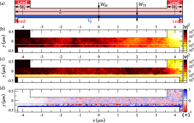
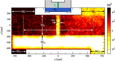
The whole system consists of a single spatially constant material, which is discretized on a square grid with a lattice spacing of . We assume the material hole doped and set the Fermi energy to , such that no quantum Hall edge states are involved in transport and the sample behaves like a conventional metal. Furthermore, Anderson disorder is added on each lattice site. The strength of this disorder is set to and the length of the strip to , which leads to a strong localization and a very low transmission between the right and the left side. The signatures of the strong localization are visible in the non-equilibrium local density of states (LDOS) in Fig. 8(b), which is calculated for a potential gradient using higher chemical potentials for the two leads at the left side. The states entering the system at the left are not able to propagate through the whole sample, which leads to a gradient in the LDOS from high densities (dark colors) at the left side to low densities (light colors) at the right side.
In the following, a quantum spin Hall effect is induced by gating a part of the material into the TI bandgap at the lower edge of the structure, as depicted by the blue region in Fig. 8(a). This results in a quantized conductance between the lower contacts, carried by a quantum spin Hall edge state, which shows up as the thin dark connection between the lower leads in the LDOS presented in Fig. 8(c). At the same time a PCC arises between the two upper leads and gives rise to quantized transport, as shown by the data in Fig. 4 of the manuscript. In comparison to the quantum spin Hall state this state is completely spread out over the whole upper part. Furthermore, the spin polarization of the PCC differs strongly from the spin polarization of the edge state. In the quantum spin Hall regime the edge state shows a very strong spin polarization, visible by the constant blue color in the spin density at the lower edge in Fig. 8(d). On the contrary the PCC has no polarization, which can be seen by the patchy pattern in the upper part of the spin density.
In the previous setup a quantized conductance was used to demonstrate the emergence of a PCC in an otherwise localized region. Therefore a very long system was needed, such that all channels, except the PCC, are sufficiently localized by the impurity potential. Although the PCC is still present if is smaller, its transport signature is masked by the additional diffusive non-localized modes. In this case an additional tunnel barrier can be used to suppress the influence of the non-perfectly conducting channels as shown in the manuscript. Therefore, we investigate the transport properties in presence of such an additional tunnel barrier, depicted by the green bar in the sketch of Fig. 9. Similar to the previous setup, a gate is used to induce a quantum spin Hall state between the lower leads and a PCC in the upper part, which can be seen in the LDOS in Fig. 9. The tunnel barrier disconnects the upper two leads and reduces the contributions of the non-perfectly conducting channels. As shown in Fig. 5 of the main manuscript, this leads to a vanishing shot noise and a quantized conductance.