Local measurement of the Eliashberg function of Pb islands: enhancement of electron-phonon coupling by quantum well states
Abstract
Inelastic tunneling spectroscopy of Pb islands on Cu(111) obtained by scanning tunneling microscopy below 1 K provides a direct access to the local Eliashberg function of the islands with high energy resolution. The Eliashberg function describes the electron-phonon interaction causing conventional superconductivity. The measured Eliashberg function strongly depends on the local thickness of the Pb nanostructures and shows a sharp maximum when quantum well states of the Pb islands come close to the Fermi energy. Ab initio calculations reveal that this is related to enhanced electron-phonon coupling at these thicknesses.
pacs:
74.25.Kc, 74.25.Jb, 73.21.-bIn conventional superconductors (SC) Cooper pairs are formed due to electron-electron interaction via virtual phonon exchange. While this concept already lies at the heart of the BCS theory Bardeen et al. (1957) it turned out soon that the simplifications by the assumptions of the BCS theory are too crude. Especially when dealing with so-called strong coupling SCs an extension of the theory is required which was presented by Eliashberg Eliashberg (1960). He took into account that the electron-phonon interaction is local in space and retarded in time. A central quantity in this theory is the effective electron-phonon spectrum , which is also called Eliashberg function. Here is the phonon density of states (DOS) and (which actually is ), is the energy dependent electron-phonon coupling strength. The Eliashberg theory allows to calculate the properties for all conventional SCs once is known.
While the experimental determination of can be achieved by inelastic neutron scattering, this technique provides no immediate access to the full Eliashberg function since it contains the electron-phonon coupling strength, which is not directly accessible with neutrons. On the other hand it was shown that the Eliashberg function can be calculated from the quasiparticle DOS of a SC extracted from tunneling experiments by inverting the Eliashberg gap equations McMillan and Rowell (1965). Although this method could confirm the validity of the Eliashberg theory it is a rather indirect way of obtaining . Especially in the case of multiple superconducting gaps, the inversion is not unique.
Inelastic tunneling spectroscopy (ITS), however, provides a direct access to the excitations in a solid. Using scanning tunneling microscopy (STM), in addition, offers the possibility of performing ITS with high spatial resolution Stipe et al. (1998). Most STM-ITS experiments were dedicated to molecular vibrations but there are, though rarely, studies of collective vibrations as well Vitali et al. (2004). The principle of ITS is based on the opening of an inelastic tunneling channel in parallel to the elastic one as soon as the energy of the tunneling electrons overcomes the threshold for performing an excitation in the sample leading to an increase of the differential conductivity . Since the latter is only of a few percent it is common to use a lock-in amplifier and record the second derivative of the tunneling current with respect to the bias voltage, , which reveals a peak at the positive voltage corresponding to the energy of the excitation. Due to the symmetry of electron and hole tunneling, a minimum (dip) is found at the same voltage on the negative bias side. A dip-peak pair is thus a characteristic fingerprint of an inelastic tunneling process. So far, we only considered excitations at discrete energies. In systems possessing a continuous spectrum of excitations, as in the case of phonons, the second derivative of the tunneling current is proportional to their DOS :
| (1) |
Here and are the electronic DOS of the tip and the sample, respectively, and are taken to be constant around . is the matrix element for inelastic tunneling which, in the case of phonons, is proportional to the electron-phonon coupling strength due to the optical theorem Cohen-Tannouji et al. (2010). In a SC, however, the formation of the gap below the superconducting transition temperature () leads to a strong energy dependence of . Since the conductance of a tunnel junction is directly proportional to the electronic DOS, the gap feature dominates the signal in . For this reason, superconductivity has to be suppressed. In principle, there are two possibilities to force a SC into its normal state even below . One is to apply a magnetic field, the other one is to use the proximity effect of a SC in contact with a normal metal.
In this Letter, we report on the first direct and spatially resolved study of the Eliashberg function by STM. We used Pb islands on Cu(111) as a model system for this novel approach and find strong dependencies of the Eliashberg function on the local electronic properties.
Pb belongs to the so-called strong coupling SCs. The value of lies far above the BCS value of 3.52 and it is the material with the strongest electron-phonon coupling among the elemental SCs Buckel (2004) and has therefore been widely studied in the past. Pb was among the systems which were investigated in the pioneering work of Giaever et al. who were able to obtain the quasiparticle DOS from planar tunnel junctions Giaever et al. (1962). Indeed, it was this measurement from which the Eliashberg function of a SC was obtained for the first time using the McMillan gap inversion method McMillan and Rowell (1965). The Eliashberg function of Pb exhibits two prominent maxima at around 4 meV and 8 meV. By regarding the phonon dispersion relation these features can be ascribed to van Hove singularities of the transverse and longitudinal phonon modes, respectively Heid et al. (2010); Brockhouse et al. (1962); Stedman et al. (1967).
In recent years, especially thin Pb islands attracted much attention since the vertical confinement of the electrons results in discrete quantum well states (QWS), which were found to have a substantial influence on the growth mode Otero et al. (2000); Su et al. (2001). When Pb is deposited onto Cu(111) at room temperature (RT), the growth mode is of Stranski-Krastanov type Camarero et al. (1998), i. e. islands start to grow once a wetting layer is complete. These islands are (111)-oriented nanocrystallites with a height distribution that is not statistical. Instead, as was first observed by Otero et al., certain ”magic” heights are strongly preferred while some other numbers of monolayers (ML) seem to be ”forbidden” Otero et al. (2002). The authors show that the appearance of these preferred heights is directly correlated to the QWS. A thickness for which a QWS is near the Fermi level is energetically unfavored and thus, when growing, the system avoids those numbers of ML. Moreover, an influence of the QWS on the electron-phonon coupling and on has been demonstrated for Pb films on semiconducting Si(111)-() Zhang et al. (2005); Guo et al. (2004); Eom et al. (2006). Different results were published, in which rises Zhang et al. (2005); Guo et al. (2004) or slightly falls Eom et al. (2006) with the film thickness superimposed with weak oscillations. In contrast, Pb islands on Cu(111) are expected to be in the normal due to the proximity effect of the metallic substrate Hilsch (1962). Hence, Pb/Cu(111) should provide an ideal system to study the phonon excitations by STM-ITS in the normal state and to resolve the details of the influence of the QWS on the Eliashberg function as well.
The preparation and study of the sample were carried out in UHV () in a home-made low temperature STM setup Zhang et al. (2011). In particular, this setup comprises a Joule-Thomson refrigerator operated with a 3He-4He mixture which allows for a base temperature below 700 mK. The Cu(111) single crystal was cleaned by sputtering with Ar+ ions at 1.5 kV and subsequent annealing at 500 . After the sample had cooled down to RT, Pb was evaporated by electron bombardment and a total amount of 3.8 ML was deposited at a rate of 1.9 ML/min. An electrochemically etched W wire, which was treated by several cycles of Ar+ sputtering and flash-annealing, was used as STM tip. The temperature of the sample and the tip was K during the measurements. For ITS the tip was stabilized at 20 mV and 50 nA and the spectra were obtained by measuring the second derivative of the tunneling current using lock-in technique Stipe et al. (1999) with a modulation voltage of 400 V (RMS) at a frequency of 16.2 kHz. Recording a single spectrum was set to take 3 min but in order to increase the signal-to-noise ratio 20 spectra were taken successively at the same point and averaged to one spectrum. These spectra are shown without any subsequent filtering.
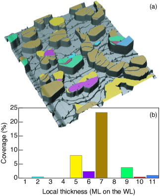
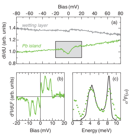
Fig. 1(a) shows a typical STM topography of the sample. Pb islands of a lateral size of about 100 nm grow on top of the wetting layer on the stepped Cu(111) surface. Most of the islands span one or more Cu steps and many of them coalesce. In order to determine the local thickness we considered the height profiles extracted from the STM topography as well as the QWS Otero et al. (2002). In Fig. 1(a) the Pb areas are marked with different colors according to their local thickness whereas Fig. 1(b) shows the thickness distribution. Most of the islands have a constant thickness of 5 or 7 ML on top of the wetting layer, which are thus the ”magic heights” for this amount of Pb. As can be seen in Fig. 1(a) and 3(a), there are, however, some islands which change their thickness by 1 or 2 ML when growing over a Cu step edge and closely spaced steps may even help to stabilize unfavored heights, as was already observed before Otero et al. (2002). In particular, there are only two rather small regions in Fig. 1(a) that are 10 ML thick and 8 ML was not observed at all.
We performed spectroscopy on the Pb regions of different heights as well as on the wetting layer. In Fig. 2 we show exemplarily the results for a Pb thickness of 12 ML. In contrast to the constant differential conductance of the wetting layer there is a pronounced dip around in the case of Pb islands. The same effect was observed for Pb islands on Si(111)-() Nishio et al. (2008); Wang et al. (2009). Since the experiment of Wang et al. was performed at 10 K, which is above of Pb, the authors termed this feature ”pseudo gap” as in the field of high temperature superconductivity. We, however, attribute the dip to inelastic excitations. We present a high resolution spectrum of this energy range in Fig. 2(b). An almost point-symmetric shape is obtained showing two dominant dip-peak pairs at a bias of about mV and mV as well as one very close to zero bias ( mV). A comparison to the previously determined Eliashberg function of Pb McMillan and Rowell (1965) is provided in Fig. 2(c) and since it reveals an almost perfect agreement there is strong evidence that the ITS data directly yields the Eliashberg function. i. e. the dip does not indicate a pseudo gap. Only the feature closest to is not related to but is due to a zero bias anomaly (ZBA), as already observed in planar tunneling experiments on Pb Wattamaniuk et al. (1971).
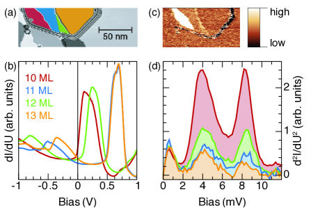
After confirming that STM-ITS is able to measure the Eliashberg function we focussed on the thickness dependence. In particular, we investigated a ”wedge”-like island (Fig. 3(a)) the height of which increases by 1 ML at every underlying step starting from 10 ML. Keeping all parameters constant, we recorded spectra (Fig. 3(d)) on every local thickness and we were able to find the ZBA and the Eliashberg function in all cases. While the former stays the same there is a strong thickness dependence of the intensity of . For areas comprising an odd number of ML it is relatively weak whereas the signal gets stronger for 12 ML and is by far strongest for 10 ML as can also be seen in the map, i. e. a map of the local electron-phonon coupling at 8 meV, in Fig. 3(c) recorded with the bias set to the energy of the longitudinal peak. No differences were found for different locations within an area of a given thickness. Note that in all experiments, the current was set to the same value during tip stabilization, such that the differences in the inelastic spectra are not related to differences in the electronic DOS. Since we expected that the thickness dependence should be influenced by the electronic QWS, we measured the first derivative of the tunneling current in a larger voltage range (Fig. 3(b)). In the case of the odd numbers of ML, the highest occupied as well as the lowest unoccupied states lie roughly 0.5 eV away from the Fermi level. In contrast, the lowest unoccupied QWS of the 10 ML and 12 ML thick layers are very close to . The relevant QWS of the former, which exhibited also the highest intensity, is closest to . Thus, our experiment clearly shows, that electron-phonon coupling can be strongly enhanced (factor 5), if unoccupied QWS are near the Fermi energy.
To elucidate the experimental finding, we calculated the electronic structure and phonons for different free standing Pb films. The structural relaxations and the phonons were computed using the VASP code, well known for precise total energy and forces calculations Kresse and Furthmüller (1996), while the electronic structure of the thin films was obtained with a first-principles Green’s function method, specially designed for semi-infinite systems such as surfaces and interfaces Lüders et al. (2001). The self-consistently calculated Green’s functions and phonons were used to compute the Eliashberg function of the given systems.
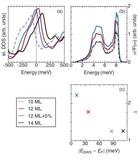
First of all, we found QWS in this systems in qualitative agreement with the experiment. The calculated electronic DOS exhibits a QWS closest to the Fermi level for a thickness of 12 ML while for 10 ML and 14 ML the QWS lie roughly 0.1 eV below and above , respectively (Fig. 4(a)). The theoretical results for in Fig. 4(b) reveal the same effect as the experiment. While the intensity of is the same for 10 and 14 ML, it increases by more than 30 % in the case of 12 ML. Also shown in Fig. 4 is the effect of compressing the surface of the 12 ML slab by 5 %. This compression shifts the QWS even closer to which again is accompanied by a further increase of the intensity of . Fig. 4(c) comprises the resulting electron-phonon coupling constant , which changes from a value of about 1.25 to 2.2, i. e. significantly above the bulk value, upon the shift of the QWS towards . Thus, in qualitative agreement to the experiment, the Eliashberg function can be increased by a QWS near the Fermi level. Quantitatively, the experimental enhancement of the electron-phonon coupling is even stronger than theoretically predicted by a factor of 2-3, possibly due to the details of the quantum well states of Pb on Cu(111).
The mechanism leading to the enhancement can be understood from total energy considerations. The formation of QWS in thin Pb films leads to an energetically unfavourable condition when a QWS lies very close to . A change of the lattice constant, e. g. by a phonon, shifts the QWS up and down through the Fermi level and leading to repopulation of the electrons with large changes of the electronic energy. Thus, deformations couple more strongly to the electronic degrees of freedom when a QWS is near the Fermi energy increasing the electron-phonon coupling. Supposed that the behavior is similar on Si(111), our findings could also explain the oscillation with the thickness as it was observed in that system Eom et al. (2006).
In conclusion, we demonstrated that, using low temperature STM-IST, it is possible to directly measure phonon excitations in Pb islands. The obtained spectra can be unambiguously identified as which allows for the experimental determination of the latter with the high spatial resolution of the STM. We found a pronounced dependence of the Eliashberg function on the thickness of the Pb slabs which, with the aid of ab initio calculations, can be explained by their energetic stability due to the position of the electronic QWS. This mechanism, if generally applicable, can be used to increase of conventional superconductors by using layered structures with QWS at appropriate energies.
M.S. acknowledges funding by the Karlsruhe House of Young Scientists (KHYS).
References
- Bardeen et al. (1957) J. Bardeen, L. N. Cooper, and J. R. Schrieffer, Phys. Rev. 108, 1175 (1957).
- Eliashberg (1960) G. Eliashberg, Soviet Physics 11, 696 (1960).
- McMillan and Rowell (1965) W. L. McMillan and J. M. Rowell, Phys. Rev. Lett. 14, 108 (1965).
- Stipe et al. (1998) B. C. Stipe, M. A. Rezaei, and W. Ho, Science 280, 1732 (1998).
- Vitali et al. (2004) L. Vitali, M. A. Schneider, K. Kern, L. Wirtz, and A. Rubio, Phys. Rev. B 69, 121414 (2004).
- Cohen-Tannouji et al. (2010) C. Cohen-Tannouji, F. Diu, and F. Laloe, Quantenmechanik 2 (de Gruyter, 2010).
- Buckel (2004) W. Buckel, Supraleitung: Grundlagen und Anwendungen (Wiley, 2004).
- Giaever et al. (1962) I. Giaever, H. R. Hart, and K. Megerle, Phys. Rev. 126, 941 (1962).
- Heid et al. (2010) R. Heid, K.-P. Bohnen, I. Y. Sklyadneva, and E. V. Chulkov, Phys. Rev. B 81, 174527 (2010).
- Brockhouse et al. (1962) B. N. Brockhouse, T. Arase, G. Caglioti, K. R. Rao, and A. D. B. Woods, Phys. Rev. 128, 1099 (1962).
- Stedman et al. (1967) R. Stedman, L. Almqvist, and G. Nilsson, Phys. Rev. 162, 549 (1967).
- Otero et al. (2000) R. Otero, A. L. Vázquez de Parga, and R. Miranda, Surface Science 447, 143 (2000).
- Su et al. (2001) W. B. Su, S. H. Chang, W. B. Jian, C. S. Chang, L. J. Chen, and T. T. Tsong, Phys. Rev. Lett. 86, 5116 (2001).
- Camarero et al. (1998) J. Camarero, J. Ferrón, V. Cros, L. Gómez, A. L. Vázquez de Parga, J. M. Gallego, J. E. Prieto, J. J. de Miguel, and R. Miranda, Phys. Rev. Lett. 81, 850 (1998).
- Otero et al. (2002) R. Otero, A. L. Vázquez de Parga, and R. Miranda, Phys. Rev. B 66, 115401 (2002).
- Zhang et al. (2005) Y.-F. Zhang, J.-F. Jia, T.-Z. Han, Z. Tang, Q.-T. Shen, Y. Guo, Z. Q. Qiu, and Q.-K. Xue, Phys. Rev. Lett. 95, 096802 (2005).
- Guo et al. (2004) Y. Guo, Y.-F. Zhang, X.-Y. Bao, T.-Z. Han, Z. Tang, L.-X. Zhang, W.-G. Zhu, E. G. Wang, Q. Niu, Z. Q. Qiu, et al., Science 306, 1915 (2004).
- Eom et al. (2006) D. Eom, S. Qin, M.-Y. Chou, and C. K. Shih, Phys. Rev. Lett. 96, 027005 (2006).
- Hilsch (1962) P. Hilsch, Z. Physik 167, 511 (1962).
- Zhang et al. (2011) L. Zhang, T. Miyamachi, T. Tomanić, R. Dehm, and W. Wulfhekel, Review of Scientific Instruments 82, 103702 (2011).
- Stipe et al. (1999) B. C. Stipe, M. A. Rezaei, and W. Ho, Phys. Rev. Lett. 82, 1724 (1999).
- Nishio et al. (2008) T. Nishio, T. An, A. Nomura, K. Miyachi, T. Eguchi, H. Sakata, S. Lin, N. Hayashi, N. Nakai, M. Machida, et al., Phys. Rev. Lett. 101, 167001 (2008).
- Wang et al. (2009) K. Wang, X. Zhang, M. M. T. Loy, T.-C. Chiang, and X. Xiao, Phys. Rev. Lett. 102, 076801 (2009).
- Wattamaniuk et al. (1971) W. Wattamaniuk, H. Kruezer, and J. Adler, Physics Letters A 37, 7 (1971).
- Kresse and Furthmüller (1996) G. Kresse and J. Furthmüller, Phys. Rev. B 54, 11169 (1996).
- Lüders et al. (2001) M. Lüders, A. Ernst, W. M Temmerman, Z. Szotek, and P. J. Durham, J. Phys.: Condens. Matter 13, 8587 (2001).