Theoretical analysis of a dual-probe scanning tunneling microscope setup on graphene
Abstract
Experimental advances allow for the inclusion of multiple probes to measure the transport properties of a sample surface. We develop a theory of dual-probe scanning tunnelling microscopy using a Green’s Function formalism, and apply it to graphene. Sampling the local conduction properties at finite length scales yields real space conductance maps which show anisotropy for pristine graphene systems and quantum interference effects in the presence of isolated impurities. The spectral signatures of the Fourier transform of real space conductance maps include characteristics that can be related to different scattering processes. We compute the conductance maps of graphene systems with different edge geometries or height fluctuations to determine the effects of non-ideal graphene samples on dual-probe measurements.
Local scattering centers such as impurities, defects and substrate inhomogeneities limit the theoretically high mobility of graphene Castro Neto et al. (2009); Chen et al. (2008); Hwang et al. (2007). Improved sample preparation and specialized substrates have improved the quality of graphene electronics Dean et al. (2010) such that even a single scatterer can influence the whole device and perhaps render it useful for, e.g. sensing applications Schedin et al. (2007); Brar et al. (2010). A detailed understanding of the influence of such defects on electronic properties is necessary in order to exploit or avoid their influence Peres et al. (2006); Peres (2010).
Information about single scatterers can be obtained via scanning tunnelling microscopy (STM), yielding direct information about the local density of states (LDOS). Previously the LDOS of graphene has been studied, both experimentally and theoretically, in the presence of defects Bena (2008); Simon et al. (2009); Amara et al. (2007); Mallet et al. (2007); Rutter et al. (2007); Peres et al. (2009); Cheianov and Fal’ko (2006); Bácsi and Virosztek (2010), edges Xue et al. (2012); Yang et al. (2010); Park et al. (2011); Barone et al. (2006); Mason et al. (2013), constrictions Bergvall and Löfwander (2013) and charge puddle formation caused by trapped molecules Deshpande et al. (2009); Zhang et al. (2009).
However, in many contexts one is interested in how the local electronic transport properties, and not just the LDOS, vary along the sample. To this aim multi-probe STM has been used to characterize a wide range of systems, including carbon nanotubes Nakayama et al. (2012), Si-nanowires Qin et al. (2012); Cherepanov et al. (2012), two-dimensional thin films Bannani et al. (2008) and graphene Cherepanov et al. (2012); Ji et al. (2012); Sutter et al. (2008). This technique analyzes nanoscale features on surfaces without the need to fabricate invasive contacts into the sample Sutter et al. (2008); Wang and Beasley (2013); Ji et al. (2012); Buron et al. (2012). Graphene is especially interesting as it is intrinsically two-dimensional and we thus probe the material properties by measuring the surface. Furthermore graphene has a long inelastic mean free path Borunda et al. (2013); Mayorov et al. (2011); Berger et al. (2006); Bolotin et al. (2008); Rickhaus et al. (2013), enabling the possibility of placing two STM tips within a length scale at which interference effects are not washed out by dephasing Nakayama et al. (2012); Baringhaus et al. (2013); Eder et al. (2013); Rickhaus et al. (2013).
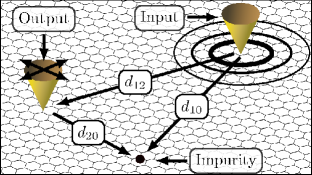
In this Letter we consider such quantum interferences as we present a theoretical analysis of the dual-probe STM setup as sketched in Fig. 1. The methodology and analysis is described for pristine graphene sheets and vacancies, but is completely general and can be easily extended to other systems. Applications to graphene systems with edges or height fluctuations are presented as examples.
Methods. – In nonequilibrium Green’s function formalism (NEGF) semi-infinite leads are coupled to a finite device region Datta (1997); Haug and Jauho (2008). We instead consider an infinite two-dimensional device connected to one fixed and one scanning STM probe as in Fig. 1 so that conventional recursive methods are not directly applicable, and an alternative approach must be used. Although we consider graphene in this work, the method is applicable to other surfaces by using the relevant Green’s Function (GF) in the following derivations. For pristine graphene in the nearest neighbour tight-binding model, the real-space single-particle equilibrium GF is given by Power and Ferreira (2011)
| (1) |
where is the energy, is the area of the first Brillouin zone, (with and integers) is the position of site , and are the graphene lattice vectors, and . The carbon-carbon hopping integral is eV Reich et al. (2002).
The zero-temperature conductance is given by the Landauer formula Datta (1997), where the transmission coefficient between the two probes is
| (2) |
() is the coupling to the probes and is the retarded/advanced Green’s function of the sample including probe effects.
Experimental STM tips have finite radii of curvature, limiting the resolution due to couplings with multiple lattice sites. We employ the Tersoff-Hamann approach Meunier and Lambin (1998); Fukuda et al. (2007); Nakanishi and Ando (2010) to describe a structureless tip with only the end orbital of a linear atomic chain coupled to the sample. The DOS of the chain is constant in the considered energy range. The coupling between the tip and a nearby lattice site is angle dependent and decays exponentially with separation 111The coupling is calculated usingMeunier and Lambin (1998); Amara et al. (2007), where , is the angle between the tip apex and site , , . is a scaling factor which we set to .. The results presented below are in broad agreement with test calculations performed for more realistic tips, where a predictable smearing of the shorter range features occurs.
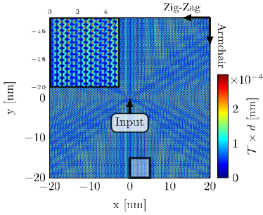
Pristine Graphene. – The transmission is obtained from Eq. (2) using a numerical evaluation of Eq. (1). The resulting map is shown in Fig. 2 for . Other Fermi energies show similar qualitative behaviour, but lower values require a larger scan area to obtain the same number of oscillation periods. In armchair directions a constant transmission is observed, while oscillations occur for zigzag directions. The results are not very sensitive to the exact position of the stationary probe, with the exponential coupling generally ensuring that the probe primarily couples to a single site.
To qualitatively understand the different behaviour for the two high symmetry directions, we exploit the fact that Eq. (1) can be approximated analytically for separations above a few lattice spacings using the stationary phase approximation (SPA)Power and Ferreira (2011). The GF can thus be written for the armchair and zigzag directions, respectively, as
| (3) |
where is an energy-dependent amplitude and is identified with the Fermi wavevector in the direction of separation between the probes.
Assuming that each probe couples only to a single site, we find, from Eq. (2), that . The transmission decays monotonically as . Correcting for this geometrical decay yields the constant transmission observed in Fig. 2 for armchair directions. The zigzag direction exhibits interference between the and terms entering in Eq. (3). As seen in the inset of Fig. 2 this leads to both long and short range oscillations. The long range oscillations depend on the Fermi wavelength. The short range oscillation on the other hand has a period of three graphene unit cells and is inherent to quantities measured along the zigzag direction and is independent of . This oscillation varies on the atomic scale and tends to get cancelled for probes coupling to many sites with different phases. However, the long range oscillations are more robust, particularly for small , as the phase is constant over a wider range of sites and should thus be observable even for tips with a larger radius of curvature. The expressions in Eq. (3) can also be used to determine the energy-dependent oscillations arising for fixed probes when a gate is applied. Thus the method described here can be easily extended for a spectroscopic mode of a dual-probe system.
Single Vacancy. The GF for a graphene system with a perturbation can be calculated using the Dyson equation,
| (4) |
where is the perturbation matrix element between site and . In principle any local perturbation can be included using this technique, and accurate parameterization for defects can be determined by comparison with density functional theory calculations Ribeiro et al. (2009); Dubois et al. (2010). The same approach is used throughout to include hopping terms between the probes and device region.
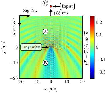
Fig. 3 shows the relative change in transmission from the pristine lattice case when a single vacancy is introduced at the origin. The vacancy and fixed probe are separated along the armchair direction and the scanning probe measures conductance fluctuations in the region around the vacancy. Quantum interference effects are clearly visible in Fig. 3. The map for a zigzag separation of fixed probe and vacancy (not shown) looks qualitatively similar. To describe the oscillations we again turn to the SPA expression for the GF. The solution of the Dyson equation for a vacancy is , where is the -matrix element of site when . Analytic solutions can be found for the scanning probe path shown by the dashed line in Fig. 3. We observe oscillations in region A, where the scanning probe is between the fixed probe and vacancy such that (see Fig. 1). From Eq. (3) we find , which exhibits oscillations. When the scanning probe is not between the fixed probe and vacancy no oscillations occur. In region B the transmission is decreased due to scattering, whereas in region C the transmission is either enhanced or decreased depending on the phase difference between the emitted and backscattered waves.
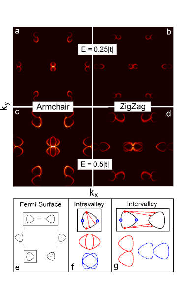
This simple analytical picture allows us to interpret the oscillations as interferences between an incoming plane wave and the backscattered wave, analogous to optical interference effects. To analyze the pattern we consider the Fourier transform (FT) of the conductance map. This approach is generally applicable to scanning images and is not limited to the graphene example. Similar procedures are often employed in the analysis of conventional STM measurements Mallet et al. (2007); Rutter et al. (2007); Deshpande et al. (2009). Fig. 4 shows the FTs of for the single vacancy at different energies and positions of the fixed probe relative to a vacancy at the origin, with Panel (a) corresponding to Fig. 3.
For the incoming wave along the (armchair) direction the double-ring patterns in Fig. 4 are the result of scattering from the top and bottom of the Fermi surface where the vectors are along the direction (indicated by red dots in Figs. 4f and 4g), to all other points (indicated with arrows) on either the same Fermi surface (intravalley, Fig. 4f) or that of the opposite valley (intervalley, Fig. 4g). The intravalley scattering produces the short wavevector features present at the center of the FT (and at all reciprocal lattice vectors), while the intervalley scattering yields the larger wavevector features at the and -points. Figs. 4a and 4b correspond to an energy in the linear dispersion regime whereas 4c and 4d show an energy with trigonal warping, thus leading to the FT signatures sketched by the diagrams of Fig. 4f-g.
Additional fine structure is seen in Fig. 4 due to deviations from the ideal picture of a plane incoming wave. Allowing a broader range of incoming -vectors increases the part of the Fermi surface which can act as an initial state. This effect is more pronounced for incoming waves along the zigzag direction where even a small broadening of the incoming -vector allows a larger part of the Fermi surface to act as an initial state. Similar calculations performed for a Gaussian shaped charge distribution, modelling a trapped charge, find that the FT scattering fingerprint is qualitatively similar to that of the single vacancy. This is in contrast to single-probe LDOS measurements, where the intervalley scattering fingerprint vanishes for extended defectsWakabayashi et al. (2007); Bergvall and Löfwander (2013).
Other Geometries. – We now consider two examples of more complicated defects: (i) A graphene sheet with an edge (Fig 5a), and (ii) a non-planar sheet with an irregular height profile (Fig 5d).
In Fig. 5a, we consider a semi-infinite graphene sheet with a pristine zigzag or armchair edge222The GF including an armchair edge, is calculated from the pristine GF with the method of images, as described in Ref. Duffy et al. (2014). For the zigzag edge a direct inversion scheme is used.. The incoming wave for the armchair edge is along the zigzag direction, and vice versa. The conductance maps (not shown) reveal oscillations away from the edge arising from the interference between incoming and backscattered waves. In contrast to the single vacancy case, not all scattering angles are available and the double-ring features in the FTs reduce to points indicating the direction of propagation (zigzag for armchair edge and vice versa) as shown in Figs. 5b and 5c. The only qualitative difference is the direction of the incoming wave and hence the direction of the scattering fingerprint in the FT. This is in sharp contrast to single-probe STM measurements, where the zigzag edge does not show an intervalley signalCasiraghi et al. (2009). The dual-probe setup thus opens the possibility of characterizing an edge by its interference pattern as both edges are equally visible with different signatures.
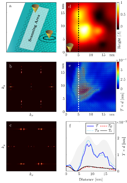
A non-planar height profile, as in Fig. 5d, affects the dual-probe measurement in two ways333Random smooth height fluctuations with amplitudes in accordance to Fasolino et al. (2007). The electronic effects can be accounted for by varying the hopping parameters according to Pereira et al. (2009) as , where is the new bond length and .. The underlying electronic properties of the system are altered by the varying bond lengths throughout the sample and secondly, the tip-sample coupling is affected by their now spatially-varying separation. The conductance map in Fig. 5e takes both of these effects into account. The signal enhancement for regions where the tip and sample are nearest suggest that it is the tip-sample separation dependent contribution which dominates. This is confirmed in Fig. 5f where we calculate the full transmission (blue) along the cross section shown by the white dashed line in Fig. 5e, with the shaded region showing the height profile along this path. In addition, we show the transmissions including the electronic contribution only, , (dashed red, calculated by mapping the changed electronic structure onto a flat surface) and the height contribution only, (dotted green, calculated by varying the tip-sample separation but leaving the sample electronic structure unchanged). We note that is a good match to the full calculation, whereas only slightly deviates from the pristine (black) curve. However, the height fluctuations considered here are not large enough to give rise to pseudomagnetic field effects like the ones considered in Ref. Juan et al. (2011). In such cases the behaviour of may provide an ideal framework to determine the effects of pseudomagnetic fields on the transport properties.
Conclusion. – The dual-probe setup offers new flexibility to study directional transport effects in nanosystems beyond the reach for a single STM probe experiment. Using graphene as a case study, anisotropic effects in the pristine material and quantum interferences around defects have been treated. The methodology developed is general and easily applicable to other materials. While the focus of this work has been on the scanning mode to reveal topographic details of the sample, an extension to the case of fixed probes and a variable gate gathering spectroscopic data is straightforward. This may be particularly useful when examining non-planar systems, where the variations due to tip-sample separation may outweigh contributions arising from the actual electronic properties of the system.
Acknowledgements The Center for Nanostructured Graphene (CNG) is sponsored by the Danish Research Foundation, Project DNRF58.
References
- Castro Neto et al. (2009) A. H. Castro Neto, N. M. R. Peres, K. S. Novoselov, and A. K. Geim, Reviews of Modern Physics 81, 109 (2009).
- Chen et al. (2008) J.-H. Chen, C. Jang, S. Xiao, M. Ishigami, and M. S. Fuhrer, Nature nanotechnology 3, 206 (2008).
- Hwang et al. (2007) E. H. Hwang, S. Adam, and S. Das Sarma, Physical Review Letters 98, 186806 (2007).
- Dean et al. (2010) C. R. Dean, A. F. Young, I. Meric, C. Lee, L. Wang, S. Sorgenfrei, K. Watanabe, T. Taniguchi, P. Kim, K. L. Shepard, and J. Hone, Nature Nanotechnology 5, 722 (2010).
- Schedin et al. (2007) F. Schedin, A. K. Geim, S. V. Morozov, E. W. Hill, P. Blake, M. I. Katsnelson, and K. S. Novoselov, Nature Materials 6, 652 (2007).
- Brar et al. (2010) V. W. Brar, R. Decker, H.-M. Solowan, Y. Wang, L. Maserati, K. T. Chan, H. Lee, c. O. Girit, A. Zettl, S. G. Louie, M. L. Cohen, and M. F. Crommie, Nature Physics 7, 43 (2010).
- Peres et al. (2006) N. M. R. Peres, F. Guinea, and A. H. Castro Neto, Physical Review B 73, 125411 (2006).
- Peres (2010) N. M. R. Peres, Reviews of Modern Physics 82, 2673 (2010).
- Bena (2008) C. Bena, Physical Review Letters 100, 076601 (2008).
- Simon et al. (2009) L. Simon, C. Bena, F. Vonau, D. Aubel, H. Nasrallah, M. Habar, and J. C. Peruchetti, The European Physical Journal B 69, 351 (2009).
- Amara et al. (2007) H. Amara, S. Latil, V. Meunier, P. Lambin, and J.-C. Charlier, Physical Review B 76, 115423 (2007).
- Mallet et al. (2007) P. Mallet, F. Varchon, C. Naud, L. Magaud, C. Berger, and J.-Y. Veuillen, Physical Review B 76, 041403 (2007).
- Rutter et al. (2007) G. M. Rutter, J. N. Crain, N. P. Guisinger, T. Li, P. N. First, and J. A. Stroscio, Science 317, 219 (2007).
- Peres et al. (2009) N. M. R. Peres, L. Yang, and S.-W. Tsai, New Journal of Physics 11, 095007 (2009).
- Cheianov and Fal’ko (2006) V. V. Cheianov and V. I. Fal’ko, Physical Review Letters 97, 226801 (2006).
- Bácsi and Virosztek (2010) A. Bácsi and A. Virosztek, Physical Review B 82, 193405 (2010).
- Xue et al. (2012) J. Xue, J. Sanchez-Yamagishi, K. Watanabe, T. Taniguchi, P. Jarillo-Herrero, and B. J. LeRoy, Physical Review Letters 108, 016801 (2012).
- Yang et al. (2010) H. Yang, A. J. Mayne, M. Boucherit, G. Comtet, G. Dujardin, and Y. Kuk, Nano Letters 10, 943 (2010).
- Park et al. (2011) C. Park, H. Yang, A. J. Mayne, G. Dujardin, S. Seo, Y. Kuk, J. Ihm, and G. Kim, Proceedings of the National Academy of Sciences 108, 18622 (2011).
- Barone et al. (2006) V. Barone, O. Hod, and G. E. Scuseria, Nano Letters 6, 2748 (2006).
- Mason et al. (2013) D. J. Mason, M. F. Borunda, and E. J. Heller, Physical Review B 88, 165421 (2013).
- Bergvall and Löfwander (2013) A. Bergvall and T. Löfwander, Physical Review B 87, 205431 (2013).
- Deshpande et al. (2009) A. Deshpande, W. Bao, F. Miao, C. N. Lau, and B. J. LeRoy, Physical Review B 79, 205411 (2009).
- Zhang et al. (2009) Y. Zhang, V. W. Brar, C. Girit, A. Zettl, and M. F. Crommie, Nature Physics 5, 722 (2009).
- Nakayama et al. (2012) T. Nakayama, O. Kubo, Y. Shingaya, S. Higuchi, T. Hasegawa, C.-S. Jiang, T. Okuda, Y. Kuwahara, K. Takami, and M. Aono, Advanced materials 24, 1675 (2012).
- Qin et al. (2012) S. Qin, T.-H. Kim, Z. Wang, and A.-P. Li, Review of Scientific Instruments 83, 063704 (2012).
- Cherepanov et al. (2012) V. Cherepanov, E. Zubkov, H. Junker, S. Korte, M. Blab, P. Coenen, and B. Voigtländer, Review of scientific instruments 83, 033707 (2012).
- Bannani et al. (2008) A. Bannani, C. A. Bobisch, and R. Moller, Review of scientific instruments 79, 083704 (2008).
- Ji et al. (2012) S.-H. Ji, J. B. Hannon, R. M. Tromp, V. Perebeinos, J. Tersoff, and F. M. Ross, Nature materials 11, 114 (2012).
- Sutter et al. (2008) P. W. Sutter, J.-I. Flege, and E. A. Sutter, Nature Materials 7, 406 (2008).
- Wang and Beasley (2013) W. Wang and M. R. Beasley, Applied Physics Letters 102, 131605 (2013).
- Buron et al. (2012) J. D. Buron, D. H. Petersen, P. Bøggild, D. G. Cooke, M. Hilke, J. Sun, E. Whiteway, P. F. Nielsen, O. Hansen, A. Yurgens, and P. U. Jepsen, Nano Letters 12, 5074 (2012).
- Borunda et al. (2013) M. F. Borunda, H. Hennig, and E. J. Heller, Physical Review B 88, 125415 (2013).
- Mayorov et al. (2011) A. S. Mayorov, R. V. Gorbachev, S. V. Morozov, L. Britnell, R. Jalil, L. A. Ponomarenko, P. Blake, K. S. Novoselov, K. Watanabe, T. Taniguchi, and A. K. Geim, Nano Letters 11, 2396 (2011).
- Berger et al. (2006) C. Berger, Z. Song, X. Li, X. Wu, N. Brown, C. Naud, D. Mayou, T. Li, J. Hass, A. N. Marchenkov, E. H. Conrad, P. N. First, and W. A. de Heer, Science 312, 1191 (2006).
- Bolotin et al. (2008) K. Bolotin, K. Sikes, Z. Jiang, M. Klima, G. Fudenberg, J. Hone, P. Kim, and H. Stormer, Solid State Communications 146, 351 (2008).
- Rickhaus et al. (2013) P. Rickhaus, R. Maurand, M.-H. Liu, M. Weiss, K. Richter, and C. Schönenberger, Nature communications 4, 2342 (2013).
- Baringhaus et al. (2013) J. Baringhaus, F. Edler, and C. Tegenkamp, Journal of Physics: Condensed Matter 25, 392001 (2013).
- Eder et al. (2013) F. R. Eder, J. Kotakoski, K. Holzweber, C. Mangler, V. Skakalova, and J. C. Meyer, Nano Letters 13, 1934 (2013).
- Datta (1997) S. Datta, Electronic Transport in Mesoscopic Systems (Cambridge University Press, 1997).
- Haug and Jauho (2008) H. Haug and A.-P. Jauho, Quantum kinetics in transport and optics of semiconductors (Springer, 2008).
- Power and Ferreira (2011) S. R. Power and M. S. Ferreira, Physical Review B 83, 155432 (2011).
- Reich et al. (2002) S. Reich, J. Maultzsch, C. Thomsen, and P. Ordejón, Physical Review B 66, 035412 (2002).
- Meunier and Lambin (1998) V. Meunier and P. Lambin, Physical Review Letters 81, 5588 (1998).
- Fukuda et al. (2007) T. Fukuda, H. Oymak, and J. Hong, Physical Review B 75, 195428 (2007).
- Nakanishi and Ando (2010) T. Nakanishi and T. Ando, Physica E: Low-dimensional Systems and Nanostructures 42, 726 (2010).
- Note (1) The coupling is calculated usingMeunier and Lambin (1998); Amara et al. (2007), where , is the angle between the tip apex and site , , . is a scaling factor which we set to .
- Ribeiro et al. (2009) R. M. Ribeiro, V. M. Pereira, N. M. R. Peres, P. R. Briddon, and A. H. Castro Neto, New Journal of Physics 11, 115002 (2009).
- Dubois et al. (2010) S. M.-M. Dubois, A. Lopez-Bezanilla, A. Cresti, F. Triozon, B. Biel, J.-C. Charlier, and S. Roche, ACS nano 4, 1971 (2010).
- Wakabayashi et al. (2007) K. Wakabayashi, Y. Takane, and M. Sigrist, Physical Review Letters 99, 036601 (2007).
- Note (2) The GF including an armchair edge, is calculated from the pristine GF with the method of images, as described in Ref. Duffy et al. (2014). For the zigzag edge a direct inversion scheme is used.
- Casiraghi et al. (2009) C. Casiraghi, A. Hartschuh, H. Qian, S. Piscanec, C. Georgi, A. Fasoli, K. S. Novoselov, D. M. Basko, and A. C. Ferrari, Nano Letters 9, 1433 (2009).
- Note (3) Random smooth height fluctuations with amplitudes in accordance to Fasolino et al. (2007). The electronic effects can be accounted for by varying the hopping parameters according to Pereira et al. (2009) as , where is the new bond length and .
- Juan et al. (2011) F. D. Juan, A. Cortijo, M. A. H. Vozmediano, and A. Cano, Nature Physics 7, 810 (2011).
- Duffy et al. (2014) J. M. Duffy, P. D. Gorman, S. R. Power, and M. S. Ferreira, Journal of Physics: Condensed Matter 26, 055007 (2014).
- Fasolino et al. (2007) A. Fasolino, J. H. Los, and M. I. Katsnelson, Nature Materials 6, 858 (2007).
- Pereira et al. (2009) V. Pereira, A. H. Castro Neto, and N. M. R. Peres, Physical Review B 80, 045401 (2009).