Scanning Tunneling Spectroscopy Study of the Proximity Effect in a Disordered Two-Dimensional Metal
Abstract
The proximity effect between a superconductor and a highly diffusive two-dimensional metal was revealed in a Scanning Tunneling Spectroscopy experiment. The in-situ elaborated samples consisted of superconducting single crystalline Pb islands interconnected by a non-superconducting atomically thin disordered Pb wetting layer. In the vicinity of each superconducting island the wetting layer acquires specific tunneling characteristics which reflect the interplay between the proximity-induced superconductivity and the inherent electron correlations of this ultimate diffusive two-dimensional metal. The observed spatial evolution of the tunneling spectra was accounted for theoretically by combining the Usadel equations with the theory of dynamical Coulomb blockade; the relevant length and energy scales were extracted and found in agreement with available experimental data.
pacs:
74.45.+c, 74.55.+v, 74.78.-w, 74.78.NaWhen a normal metal (N) is in close proximity to a superconductor (S), it acquires genuine superconducting properties which are reflected in the modification of its local density of states (DOS). This phenomenon, known as proximity effect, has been studied for decades deGennes1964 and is used nowadays in various superconducting quantum devices Cleuziou2006 ; Giazotto2010 . Most of the experimental studies of the proximity effect have focused on the analysis of three-dimensional diffusive metals Pannetier2000 , whereas reports on two-dimensional (2D) systems are scarce. Due to reduced screening, enhanced electron correlations, and localization at low temperatures, the proximity effect in 2D metals is expected to be drastically modified. However, not much is known about the interplay between superconducting correlations induced by proximity and electron correlations in disordered 2D metals. The central goal of this work is to shed new light on this fundamental issue.
So far, apart from notable exceptions Gueron1996 ; Moussy2001 ; Escoffier2004 ; leSueur2008 , most of the reported experiments did not provide spatially-resolved information on the proximity effect. This is mainly due to the difficulties on applying Scanning Tunneling Microscopy/Spectroscopy (STM/STS) techniques to ex-situ elaborated (and thus, surface-contaminated) mesoscopic systems. On the other hand, the progress in the controlled growth of atomically clean superconducting materials under ultrahigh vacuum has opened the possibility to probe the proximity effect in in-situ STM/STS experiments with high spatial and energy resolution. Very recently, Kim et al. Kim2012 reported a STM/STS study in a system consisting of 5 monolayer (ML) thick superconducting Pb islands grown on Si(111) and an atomic overlayer of the striped incommensurate (SIC) phase of Pb. Unfortunately, the analysis of the proximity effect in the SIC layer was performed at relatively high temperatures ( K) and thus, the energy resolution was rather limited. More importantly, this experiment did not reveal any specific feature related to the low-dimensionality of the SIC layer. Besides, SIC phase Pb/Si(111) becomes superconducting below K and thus, it is not an ideal system where to study the proximity effect.
In this Letter we explore experimentally and theoretically the proximity effect in a highly diffusive atomically-thin metal. The samples were grown in situ by deposition at room temperature of a few atomic layers of Pb onto an atomically clean reconstructed surface of undoped Si(111). The topographic STM images in Fig. 1(a) revealed the resulting Pb network consisting of atomically flat 7-13 ML thick single nano-crystals of Pb, interconnected by a 1-2 ML thick wetting layer (WL) of Pb Budde2000 . In Fig. 1(b) the experimental geometry is sketched; the regions of interest include the island edge and the neighboring part of the WL. The experiments were performed in ultra-high vacuum mbar and mechanically sharpened Pt/Ir tips were used. In order to resolve fine spectroscopic features, the STM/STS experiments were conducted at mK, i.e. at Brun2009 . Local tunneling conductance spectra were derived from the raw data.
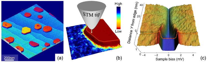
Our main finding is illustrated in Fig. 1(c) where we show the evolution of local spectra as a function of the distance from the island edge. The superconducting state in the islands is characterized by a fully opened gap (bottom curve in Fig. 1(c)), which is spatially homogeneous over the island area (red-colored in the STS map Fig. 1(b)). On the WL side far from the islands, the zero-bias conductance is high, and the tunneling spectra in these regions exhibit a V-shaped dip at zero-bias (upper curve in Fig. 1(c)), which from now on will be referred to as a zero-bias anomaly (ZBA). The absence of a clear gap is an evidence of the intrinsic non-superconducting character of the WL Non-supercond WL . As the STM tip approaches the island edge, the tunneling spectra evolve gradually from the non-superconducting ZBA to the superconducting gap shape thus evidencing the proximity effect on a scale of several nanometers (detailed conductance maps are presented in supplementary material SM ).
Let us first discuss the origin of the ZBA in the tunneling spectra of the WL which is, taking into account its thickness and the absence of conduction electrons at low temperatures in the undoped Si substrate, an ideal case of a disordered 2D conductor. Indeed, among the reported Pb-Si systems, the atomically disordered Pb WL Budde2000 is characterized by an increased roughness in STM images ( nm in Fig. 2(b)) and lack of atomic ordering. This is at variance with the Pb islands which have smooth and perfectly ordered surfaces, see Fig. 2(a). In Fig. 2(c) we present a characteristic tunneling spectrum taken in the WL far enough from the islands, to avoid the proximity effect. The shape of this ZBA resembles the diffusive anomalies found in tunneling junctions between disordered conductors Altshuler1985 . In those junctions, the suppressed tunneling conductance at low bias is attributed to the reduction of the electron tunneling DOS around the Fermi energy caused by the electron-electron interaction Altshuler1985 . Similar anomalies appear in ultrasmall tunnel junctions due to dynamical Coulomb blockade (DCB) Devoret1990 ; Girvin1990 ; Grabert1992 ; Brun DCB , i.e. due to the interaction of the tunneling electrons with the electromagnetic environment in which the junction is embedded Grabert1992 . Indeed, these two phenomena have been shown to be two sides of the same coin Nazarov1989 ; Ingold1992 ; Rollbuehler2001 . In particular, Rollbühler and Grabert Rollbuehler2001 have demonstrated that the tunneling into a disordered 2D conductor is formally equivalent to the DCB in an ultrasmall junction with an Ohmic environment. In view of this mapping, we shall use here the standard DCB theory detailed in Ref. [Ingold1992, ] to describe the tunneling spectra in the normal part of the WL. Within this theory, the tunneling current is given by , where the inelastic tunneling rates can be expressed as
| (1) | |||||
and . Here, is the tunneling resistance, is the Fermi function, is the normalized local DOS of the wetting layer, and is the probability for an electron to emit the energy into the electromagnetic environment Ingold1992 . Notice that we have assumed that the tip has an energy-independent DOS. The function is calculated using the total impedance , where and are the effective capacitance and resistance of the WL, respectively, see Fig. 2(d). The STM junction capacitance, aF Brun DCB , was neglected here.
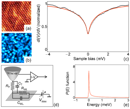
In Fig. 2(c) we show as a solid line the best fit of the experimental ZBA using the DCB theory just described. To obtain this fit by means of Eq. (1), both and were used as adjustable parameters, while the DOS of the WL was assumed to be the one of the non-interacting normal state, i.e. . The best fit for the experimental temperature was obtained with aF and k. The latter value is quite reasonable: It is close to yet lower than the quantum of resistance k, as expected for a correlated 2D metal manifesting an Altshuler-Aronov ZBA Altshuler1985 . The value is also consistent with previous in-situ transport measurements Pfennigstorf2002 . The value of the capacitance is more difficult to interpret. It is about three orders of magnitude higher than the estimated self-capacitance aF of individual Pb nano-domains in Fig.2(b), and almost two orders of magnitude larger than . This clearly indicates that the characteristic length scale involved in the charging effects is much larger than the typical nanometer-size of a domain or of the tunneling junction and thus, is indeed related to the WL. Finally, the quality of the fit in Fig. 2(c) strongly supports that it is possible to render satisfactorily the tunneling data on the basis of the DCB theory using a minimalistic effective RC environment.
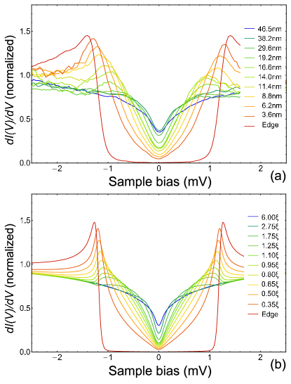
We now turn back to the spatial evolution of the tunneling spectra within the proximity region shadow-effect . As the tip is moved away from the island and starts probing the WL, the tunneling conductance rapidly evolves, see Fig. 3(a). At short distances, the peak-to-peak separation smoothly reduces, the gap rapidly fills with quasiparticle states at the gap edges, while at zero-bias remains low. At larger distances from the island, the peak-to-peak separation reduces further, the quasiparticle peaks rapidly smear out and reduce in height. Moreover, the whole tunneling characteristics inside the gap become more and more V-shaped, and the conductance at zero bias gradually increases. Finally, 40-50 nm away from the island the local spectra become peak-less and the ZBA of Fig. 2(c) is recovered (for 2D STS maps see Ref. [SM, ]).
The theoretical description of the proximity effect in a correlated normal metal is challenging and, although considerable progress has been made in this direction Oreg1999 , there does not exist suitable theory that can be directly applied to our hybrid system. In order to explain our experimental results, and inspired by Ref. [Gueron1996, ], we shall use here an heuristic extension of the DCB theory discussed above. Our assumption is that the proximity effect can be described by computing the DOS of the WL in Eq. (1) with the help of the Usadel equations Usadel1970 . Let us recall that the Usadel theory has been very successful explaining the physics of conventional diffusive SN junctions Gueron1996 ; leSueur2008 ; Belzig1996 . To be precise, we model our system by means of a SN junction, where N is an infinite normal wire and S is an ideal BCS superconducting reservoir with a gap . We also assume that the SN interface is perfectly transparent and we neglect the inverse proximity effect in the S reservoir (see Ref. [SM, ] for more details). In this model, the superconducting correlations penetrate in the normal metal a distance that depends on energy as , where is the diffusion constant in the metal.
To describe the results of Fig. 3(a), we use the function obtained in the analysis of the normal state of the WL, see Fig. 2(e), which is now kept fixed. The superconducting gap is also fixed to meV from the best fits of the spectra on the Pb island Nishio ; Cren ; the distance to the SN interface is measured in units of the length . Thus, the remaining adjustable parameter is the diffusion constant entering this expression, which must have the same value for all spectra. In Fig. 3(b) we present a set of numerically generated curves; the best match with experimental data is achieved with nm resulting in cm2/s. Notice that the computed spectra reproduce nicely the above discussed spatial evolution of the experimental tunneling data, including even very fine shape variations note . Moreover, the value of extracted here is in good agreement with the value inferred from in-situ conductance measurements of these 1-2 monolayer thick WL Pfennigstorf2002 . Let us emphasize that the diffusion constant in our case is more than one order of magnitude smaller than in conventional metals Gueron1996 ; leSueur2008 , which confirms that we are dealing with a highly disordered system (still away from the metal-insulator transition, ).
In conclusion, in a very low temperature STM/STS experiment we revealed the proximity effect between superconducting Pb islands and an ultimate disordered 2D metal - a non-superconducting Pb wetting layer grown on undoped Si(111). We found the tunneling spectra to evolve, on a scale of several nanometers, from a superconducting bulk-like behavior inside the islands to a peculiar V-shaped zero-bias anomaly far away from them. We attributed this behavior to the interplay between disorder and electron correlations in the wetting layer. We developed a phenomenological combination of the DCB theory and the Usadel model to explain these observations. Our findings not only provide a novel insight into the physics of proximity effect, but they also pave the way for studying new aspects of this effect in a great variety of hybrid systems including in-situ fabricated lateral SNS junctions in which the correlations play an important role.
We thank Hermann Grabert for useful discussions. This work was supported by grants from the University Pierre et Marie Curie (UPMC) “Emergence” and by CNRS PhD grant (L.S.-G.). J.C.C. and F.S.B. acknowledge financial support from the Spanish MICINN (Contracts No. FIS2011-28851-C02-01 and FIS2011-28851-C02-02).
References
- (1) P.G. de Gennes, Rev. Mod. Phys. 36, 225 (1964).
- (2) J.-P. Cleuziou, W. Wernsdorfer, V. Bouchiat, T. Ondarçuhu, M. Monthioux, Nature Nanotechnol. 1, 53 (2006).
- (3) F. Giazotto, J.T. Peltonen, M. Meschke and J.P. Pekola, Nature Phys. 6, 254 (2010).
- (4) B. Pannetier and H. Courtois, J. Low Temp. Phys. 188, 599 (2000).
- (5) S. Guéron, H. Pothier, N.O. Birge, D. Esteve, and M.H. Devoret, Phys. Rev. Lett. 77, 3025 (1996).
- (6) N. Moussy, H. Courtois, and B. Pannetier, Europhys. Lett. 55, 861 (2001).
- (7) W. Escoffier, C. Chapelier, N. Hadacek, and J.-C. Vill gier, Phys. Rev. Lett. 93, 217005 (2004).
- (8) H. le Sueur, P. Joyez, H. Pothier, C. Urbina, and D. Esteve, Phys. Rev. Lett. 100, 197002 (2008).
- (9) J. Kim, V. Chua, G.A. Fiete, H. Nam, A.H. MacDonald, and C.-K. Shih, Nature Phys. 8, 464 (2012).
- (10) K. Budde, E. Abram, V. Yeh, M. C. Tringides, Phys. Rev. B 61, R10602 (2000).
- (11) C. Brun et al., Phys. Rev. Lett. 102, 207002 (2009).
- (12) By applying an external magnetic field up to 6 T we additionally checked the absence of vortices in the WL and, more importantly, a general insensitivity of the ZBA spectra to the magnetic field.
- (13) See supplemental material at http://link.aps.org/supplemental/PRL/v110/i15/e157003
- (14) B.L. Altshuler, and A.G. Aronov, in Electron-Electron Interactions in Disordered Systems, edited by A.L. Efros and M. Pollak (Elsevier Science Publisher B.V., Amsterdam, 1985); P.A. Lee and T.V. Ramakrishnan, Rev. Mod. Phys. 57, 287 (1985).
- (15) M. H. Devoret et al., Phys. Rev. Lett. 64, 1824 (1990).
- (16) S. M. Girvin et al., Phys. Rev. Lett. 64, 3183 (1990).
- (17) Single Charge Tunneling, edited by H. Grabert and M. Devoret, NATO ASI, Ser. B, Vol. 294 (Plenum, New York, 1992).
- (18) C. Brun et al., Phys. Rev. Lett. 108, 126802 (2012).
- (19) Yu.V. Nazarov, Zh. Eksp. Teor. Fiz. 95, 975 (1989) [Sov. Phys. JETP 68, 561 (1990)].
- (20) G.-L. Ingold and Yu.V. Nazarov, in Ref. Grabert1992, , p. 21.
- (21) J. Rollbühler and H. Grabert, Phys. Rev. Lett. 87, 126804 (2001).
- (22) O. Pfennigstorf, A. Petkova, H.L. Guenter, and H. Henzler, Phys. Rev. B 65, 045412 (2002).
- (23) Note that due to the finite size of the STM tip apex, the WL in the vicinity of the Pb-island edge is not accessible by STS. Within this “shadow” region of a few nm the tip does not probe the WL but rather the upper edge of the island (see Ref. [SM, ]).
- (24) Y. Oreg, P.W. Brouwer, B.D. Simmons, and A. Altland, Phys. Rev. Lett. 82, 1269 (1999); M.A. Skvortsov, A.I. Larkin, and M.V. Feigel’man, Phys. Rev. B 63, 134507 (2001); A.G. Semenov, A.D. Zaikin, and L.S. Kuzmin, Phys. Rev. B 86, 144529 (2012).
- (25) K.D. Usadel, Phys. Rev. Lett. 25, 507 (1970).
- (26) W. Belzig, C. Bruder and G. Schön, Phys. Rev. B 54, 9443 (1996).
- (27) T. Nishio et al., Phys. Rev. Lett. 101, 167001 (2008).
- (28) T. Cren et al., Phys. Rev. Lett. 102, 127005 (2009); Phys. Rev. Lett. 107, 097202 (2011).
- (29) Notice, however, that the agreement is not perfect, which shows the limitations of our simple model where a fixed RC environment was used to describe all the experimental curves of Fig. 3(a).