Measurement errors in entanglement-assisted electron microscopy
Hiroshi Okamoto
Department of Electronics and Information Systems,
Akita PrefecturalUniversity, Yurihonjo 015-0055, Akita, Japan
Electronic address: okamoto@akita-pu.ac.jp
PACS: 67.81Ee, 34.80.Gs, 61.80.-x, 06.20.Dk
The major resolution-limiting factor in cryoelectron microscopy of unstained biological specimens is radiation damage by the very electrons that are used to probe the specimen structure. To address this problem, an electron microscopy scheme that employs quantum entanglement to enable phase measurement precision beyond the standard quantum limit has recently been proposed [Phys. Rev. A 85, 043810]. Here we identify and examine in detail measurement errors that will arise in the scheme. An emphasis is given to considerations concerning inelastic scattering events because in general schemes assisted with quantum entanglement are known to be highly vulnerable to lossy processes. We find that the amount of error due both to elastic and inelastic scattering processes are acceptable provided that the electron beam geometry is properly designed.
I Introduction
In cryoelectron microscopy, unstained biological specimens are rapidly vitrified at cryogenic temperatures [1, 2]. Consequently, artefacts due to heavy-metal staining, desiccation, and other sample preparation processes are no longer an issue. However, the frozen, hydrated biological specimen, consisting mostly of light elements, scatters electrons weakly. Hence biological specimens generally are weak phase objects associated with low image contrast [3]. In this setting, the resolution is limited by radiation damage by the probe electrons [4] to approximately 5-10 nm in the case of single objects [5]. This leaves much to be desired because 2 nm resolution would be needed to identify molecules in frozen vitrified slices of the cell in cryoelectron tomography [6], or 0.8 nm resolution would be required to observe the secondary structure of a single protein molecule. The reason why radiation damage limits the resolution is that the ’safe’ electron dose, which does not cause sizable damage to the specimen, is so small that the low-contrast image is dominated by shot noise. Shot noise is a manifestation of the particle nature of the electron and hence is fundamental.
Several approaches to address the radiation damage problem are known. First, methods based on averaging, such as two-dimensional crystallography [7] and single-particle analysis [8], represent an established branch of methodology in structural biology. In favorable cases, these methods essentially attained atomic resolution [9]. However, in order to average out the noise, this approach requires at least thousands of copies of the molecule of interest without much structural variance and hence is not suited for soft or unique objects. Second, the advent of in-focus phase contrast electron microscopy [10, 11, 12] enabled researchers to see weak phase objects much clearer than hitherto possible. The reason is that it provides a well-behaving phase contrast transfer function (CTF) that does not fall to zero at low resolutions and does not oscillate at high resolutions. However, this method does not go beyond the standard quantum limit, as will be mentioned. Third and finally, the use of low acceleration voltage down to, e. g. 20 kV reduces radiation damage. In particular, one may choose the electron energy below the onset of relevant knock-on damage thresholds, although the dominant damage mechanism in biological cryoelectron microscopy is considered to be ionization events due to radiolysis [13]. There have recently been much effort on developing aberration-corrected low-voltage transmission electron microscopes (TEMs) and scanning TEMs (STEMs) around the globe [14, 15, 16]. While this approach certainly makes sense, the inelastic mean free path is considerably shorter at lower electron energies, necessitating preparation of ultra-thin specimens [17]. While there have been reports of impressive images of thin biological molecules [18] and organic molecules [19] since decades ago, hydrated macromolecules of biological interest can have the size more than 50 nm. This makes it necessary to study thicker specimens and hence, if we insist on studying biologically interesting frozen hydrated macromolecules or vitrified slices of the cell, the use of a sufficiently high acceleration voltage is necessary. Overall, these considerations suggest that no current electron microscopy method produces, in a robust and widely applicable manner, images of single hydrated objects of biological interest at a resolution below 2 nm. Furthermore, phase measurement in all electron microscopy methods developed thus far, including all mentioned above, is governed by the shot noise limit, or in other words, the standard quantum limit. In this case, the precision of the measurement of the small phase shift , associated with the biological specimen, scales with the number of electrons as .
That the standard quantum limit can be beaten is well known in the field of quantum metrology [20]. While the field has begun decades ago [21, 22], a sizable fraction of recent activities in quantum metrology, mostly in the context of optics, revolves around the idea of employing entangled quantum states [23, 24, 25]. In particular, measurement of a phase shift is a familiar objective in quantum metrology and it is relevant also to biological electron microscopy where weak phase objects are dealt with. A major question in quantum metrology is how the measurement precision varies with the amount of relevant ’resources’ . Among others, ’query complexity’ emerged as one of the most useful ’resource count’ [26], which has been further elucidated and shown to be governed by the Heisenberg limit [27]. Roughly, the number of queries equals the number of interactions with the entity to be measured. Hence query complexity nicely captures the resource in biological electron microscopy, where the experimenter wants to get the most out of each ’query’, which corresponds to passing of each electron in the specimen. It is worth noting here that, notwithstanding the recent theoretical [28] and experimental [29] reports of beating the Heisenberg limit, as long as the number of query is taken as the resource count, the Heisenberg limit does represent the fundamental limit [27].
It should be noted that the Heisenberg limit is by no means an easy target in real situations [30]. It has increasingly been recognized that entanglement-assisted measurement is vulnerable to lossy processes and a number of recent studies address this problem [31, 32, 33, 34]. It is now established that quantum metrology, in lossy situations, offers ’merely’ a constant-factor improvement in the measurement precision, as opposed to the quadratic asymptotic improvement by a factor proportional to . Nevertheless, a constant-factor improvement is all that we want in biological electron microscopy, or perhaps in any measurement for that matter. The real question is whether the value of the constant factor enables relevant specific resolutions, such as aforementioned 2 nm or 0.8 nm. This requires an analysis specific to biological cryoelectron microscopy, but in doing so, we may learn lessons of more general character.
On a related note, a recent work [35] proposes an efficient multi-pixel phase estimation method that takes advantage of quantum entanglement. While interesting, the scheme employs a delocalized probe state over all the pixels and hence it is unlikely to be robust against localizing lossy processes, which occur in biological electron microscopy.
It should also be noted that, in general, beating the standard quantum limit does not necessarily require an entangled quantum state [36]. Repeated use of a probe particle would suffice. However, in the present case of entanglement-assisted biological electron microscopy, entangled quantum states are necessary for a somewhat mundane reason that the repeated use of an electron would result in too large a scattering angle to be handled by practical electron optics.
The use of quantum advantage specifically in the context of biological electron microscopy has been discussed for some time now, albeit mostly from the theoretical perspective [37, 38, 39, 40, 41, 42]. In this paper we build on the recently proposed scheme that uses quantum entanglement between the probe electron and the Cooper pair box (CPB) placed on an electron mirror [42]. The scheme realizes what effectively amounts to multiparticle entanglement between the probe electrons, by way of sequential interactions between each electron and the CPB. A major objective of this paper is to investigate how and to what extent the effect of lossy processes may be mitigated in the proposed scheme.
A distinct quantum approach [40] to biological electron microscopy based on interaction-free measurement [43, 44], also suggested in Ref. [39], has been proposed. While interesting, we note that there is certain limit associated to this type of approach [45].
This paper is organized as follows. We first review the entanglement-assisted electron microscopy scheme in Sec. II. This is followed by Sec. III, in which we deal with errors that is not related to lossy processes. In Sec. IV, we study how inelastic scattering processes make adverse effects to the scheme. We also show that an appropriate design of the electron probe geometry enables us to combat this type of effect. Sec. V concludes the paper. Symbols respectively denotes the absolute value of the electron charge and the electron mass. A diffraction plane refers to any plane conjugate to the back focal plane of the objective lens. Since aberration-corrected electron optics is becoming a commonplace, we generally neglect lens aberrations unless explicitly stated otherwise. The probe electron energy is assumed to be throughout the paper.
II Electron microscopy assisted by quantum entanglement
A A brief review
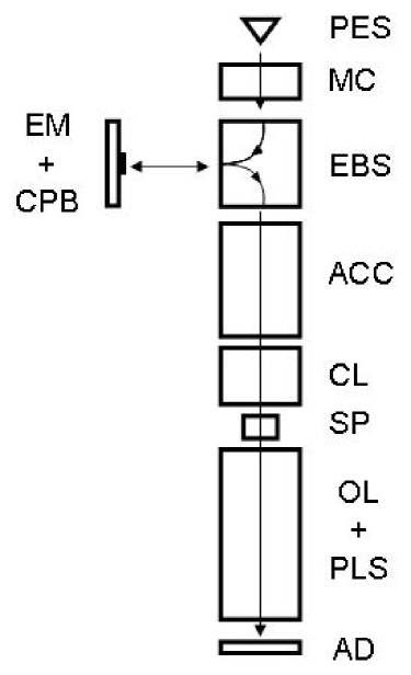
Here we briefly review the microscope proposed in Ref. [42], in part because we also want to fix notations [46]. The scheme takes advantage of superconducting quantum electronics that includes a single CPB [47], presumably in the circuit quantum electrodynamics configuration [48]. The microscope is designed to measure the difference of phase shifts and that are respectively associated with two regions and on the biological specimen, which generally is a weak phase object. Multitude of such a measurement form an image. On the face of it, the shapes of the two regions and may be chosen arbitrarily: For example, they may be adjacent two small pixels, or it may be that surrounds a smaller region . However, we will find in the present work that the latter choice is much better. The CPB is placed on the surface of an electron mirror, which in turn is inserted between the pulsed electron gun and the condenser lens so that the electron emitted from the electron gun first interacts with the CPB before going to the specimen (See Fig. 1). We use only two states and of the CPB, that respectively denote quantum states of the CPB with zero or one excess Cooper pair, where the subscript ’b’ stands for the word ’box’. The main function of the electron mirror in this scheme is to modify the electron beam shape, depending on the charging state of the CPB: The electron mirror is designed in such a way that the beam trajectory is so sensitive to the CPB charge state that only a single Cooper pair in the CPB is sufficient to direct the electron beam to the specimen region that would otherwise go to . The scattered electrons then go through more or less ordinary electron optics and are detected at a plane, which is not conjugate to the image plane, by an area detector with high quantum efficiency. Alternatively, unlike the case of Ref. [42], we will assume that the probe electrons are detected on a diffraction plane in the present work. In this case, it may well be possible to get rid of the objective lens (OL) and the projector lens system (PLS) shown in Fig. 1 altogether, resulting in an instrument resembling the scanning TEM (STEM).
We mention several engineering challenges involved. A more complete discussion of most of what follows has been presented elsewhere [42]. There are mainly five aspects that need to be developed. First, while the electron mirror has long history, an electron mirror that works at temperatures generated by the dilution refrigerator, i.e. a few tens of millikelvin, must be developed. Second, a pulsed electron gun [49], with energy spread and ps pulse width, must be developed. Each pulse may or may not contain an electron for the scheme to work. We note that energy spread has already been realized in the field of high resolution electron energy loss spectroscopy (HREELS) where very low energy () electrons are dealt with [50]. In a similar fashion, the part of the electron optical system shown in Fig. 1, consisting of the pulsed electron source, monochromator, electron beam separator and the electron mirror, controls electrons with such low kinetic energy. Unlike the case of TEM-EELS, we do not need a several hundred keV high voltage source with the voltage stability comparable to the energy spread () of the electron beam. Third, the Cooper pair box on the electron mirror must be operated in a controlled fashion and such operations must be synchronized with the pulsed electron gun. Fourth, as noted earlier, the electron optical system must be sensitive enough so that a single excess Cooper pair in the Cooper pair box can be ’seen’ with the electron optics. Fifth and finally, after interacting with the Cooper pair box, the probe electron must be accelerated to several hundred keV before interacting with the biological specimen. In principle, this can be done by brute force, i.e. by electrically floating a large part of the electron microscope on either side of the accelerator ACC shown in Fig. 1 by several hundred kilovolts [42]. A recent development in this connection, on the other hand, is the use of radio-frequency accelerator that has been applied to TEMs [51, 52] and it seems to have good compatibility with a pulsed electron beam. If this approach moves beyond the proof-of-principle stage, then it will be unnecessary to electrically float such a large part of the microscope as described above.
We describe the single electron process that lies at the heart of our method. As shown later, mutiple single electron processes ( of them) will comprise a k-electron process in our scheme. The single electron process involves a single imaging electron and proceeds as follows. Suppose that the CPB is in a superposed charge state
| (1) |
before the electron from the electron gun approaches the CPB. After the electron interacts with the CPB, it gets entangled with the CPB so that the whole quantum state of the CPB-electron system is
| (2) |
where the electron states and respectively denotes electron waves incident on and regions on the specimen. Upon transmission through the specimen, the electron wave in the state acquires a phase factor relative to the state , corresponding to the phase shift . Hence the state becomes . Let the electron state represent a diffracted wave to the -th pixel of the area detector. We expand the electron states in terms of these states as
Using these, we obtain another expression of the state as
Upon detection of the electron at the -th pixel of the area detector, the CPB is left in the state
| (3) |
where is a real normalization factor.
In reality, an electron wave is not a qubit. One way to make the above argument somewhat more precise is to expand the state as
where each state on the right hand side is spatially more localized on the specimen than the state is. The state becomes, after transmission through the specimen,
In this case, the above phase shift value would represent something similar to, but not identical with, the average of . This way of representation would be more suitable when we deal with a specimen with a structure within the region of the electron beam. However, we will not pursue this representation. The point is also related to the similar intensity map condition [42], to which we now turn.
To simplify the analysis, we assume that , which amounts to saying that the electron waves from the two small regions have similar intensity on the area detector. This assumption is what we call the similar intensity map condition. The assumption appears to be natural, but to what extent the similar intensity map condition is satisfied must be carefully evaluated, which will be done in Sec. III. Once we accept , we may write , where represents a known phase shift associated with the optical path length difference between two electron trajectories, starting respectively at the specimen regions and ending at the -th pixel of the area detector. The CPB state (3) may then be expressed as, up to the overall phase factor,
| (4) |
Since we know , by quantum information processing machinery developed for the CPB [48] we may nullify it to obtain
| (5) |
Let us call this last step as the phase compensation step. Comparing equations (1) and (5), we see that, assuming that the similar intensity map condition is satisfied, the net effect induced by the single electron process is multiplication of the phase factor to the CPB state relative to .
The k-electron process in our scheme consists of, in the order of execution, the CPB initialization step, repeated single electron processes that is described above ( times), and the CPB readout step. First, the CPB is initialized to the state . Second, the single electron process is repeated times, resulting in the state
| (6) |
This state may be expressed as, up to the overall phase factor,
where and . Finally, in the CPB readout step we measure the CPB state with respect to the basis . Probabilities to find the state in these basis states are respectively
| (7) |
Notice, by the way, that the correction step between the states (4) and (5) within the k-electron process may collectively be postponed until right before the CPB readout step. In this case, all phase correction values are recorded; and their sum is used in the combined correction step.
We show how the Heisenberg limit can be approached. We write the electron dose for a measurement on a single spot on the specimen , which must be kept below a certain value in order not to damage the specimen significantly. Hence we can repeat the k-electron process times (that we assume to be an integer for simplicity). As is well known from the theory of binomial distribution, the random variable representing the number of finding the CPB state in the state has the expectation value and variance . To simplify the analysis, we assume that , although this may not necessarily be a good approximation in some of actual settings. Then we obtain and . Introducing another random variable , we have
Hence, the expected error in determining with the k-electron process is . Note that this represents the standard quantum limit when and the Heisenberg limit when .
B Several remarks
We remark that, despite being sequential, our scheme may also be regarded as one using something akin to the bosonic NOON state [53]. Suppose that we had an unusually long electron microscope column between the CPB-incorporated electron mirror and the specimen. Then all electrons would be flying simultaneously in the column before any of them colliding with the specimen. From the discussions above, we see that these electrons would be in the state
where denotes the state in which all electrons are in the state , and likewise for .
There are at least three sources of errors in the scheme reviewed in this section. First, to what extent the similar intensity map condition holds should be investigated, as remarked above. If this condition is significantly violated, then the absolute values of the coefficients in equation (1) deviate from the ideal , making the ’contrast’ of the final measurement weaker. Second, when inelastic scattering happens, which is indeed times more likely to happen than the elastic counterpart in cryoelectron microscopy [7, 62], we lose some coherence in the CPB state. In particular, if the inelastic event is localized, then the specimen would ’measure’ the probe electron state with respect to the localized basis states . In this case, the coherence would be completely lost. However, the actual situation is subtler and we will investigate how things should behave. Third, we have not thoroughly analyzed the CPB-electron entangling interaction to estimate what and how much errors would be introduced when the electron bounces off the CPB in the electron mirror. We will consider the first two sources of errors in this paper, while leaving the last item for future analysis.
What frequency of faulty measurement can we tolerate? To get a rough idea, let us simplify the situation and consider a totally destructive event that projects the CPB state onto either or . Suppose that such a destructive event occurs at random with the probability . The number of k-electron process is and any k-electron process fails if a destructive event occurs more than once during single electron processes. (For simplicity, we assume that the experimenter, being somewhat lazy, does not abort the k-electron process upon such a destructive event.) The success probability of a k-electron process is if is sufficiently small. The number of k-electron processes for the same dose is . Retracing the argument in the previous subsection A, we have the expectation value , variance , , and eventually
| (8) |
We want the variance smaller than the variance in the conventional case . To find that minimizes the ratio , we differentiate this expression and equate the result to zero. We find and this result remains valid when, e. g., we minimize the ratio of standard deviations instead of . When errors are not totally destructive, the error will still accumulate in the random-walk-like fashion and will eventually become totally destructive. In this case, we may redefine accordingly (which we do not do in this paper) so that, on average, it takes approximately single electron processes for the accumulated error to be fully destructive.
Finally, we remark on relativistic effects. Since the TEM we have in our mind may well operate at voltages as high as 300 keV, there will be relativistic effects. In the rest of the paper we use the so-called relativistically corrected Schrodinger equation, which is a good approximation to the Dirac equation in our case [54]. The equation is the standard time-independent Schrodinger equation, but the mass and the energy are interpreted respectively as and , where , , is the electron rest mass, and is the relativistic electron energy including the rest energy .
III Errors due to coherent processes
In this section, we study the extent to which the similar intensity map condition is satisfied, for two cases of the probe electron beam geometry.
A Focused incident beam
First we study a simple case, in which the two regions and are adjacent two small regions of the same size of . We consider a thick specimen. We assume that the electrons are detected on a diffraction plane. Then the problem is effectively about the diffraction pattern from a small spot and the question is how smooth the intensity on the detector is. Let us focus on the region . Let the -axis be parallel to the direction of the incident wave propagation and let the position of the specimen be at . Atoms in the specimen are labeled by an integer and are respectively located at . Let be the scattering amplitude of the -th atom corresponding to its elemental identity. We assume the electron waves to be monochromatic and write the wavenumber . We ignore multiple scatterings in the specimen. We want the incident beam to be Gaussian with the waist size and assume that the diffraction-limited waist of the Gaussian beam is on the specimen. Without loss of generality, we compute the wave amplitude at a point P in the far field on the -plane, where is large and coordinate is given by . Far from the specimen, the transmitted Gaussian wave has the known form in the paraxial approximation (See Appendix A)
| (9) |
that can be approximated as
| (10) |
Consider a single elastic scattering event. The amplitude of the scattered wave at the point P is found to be (See Appendix A)
| (11) |
For simplicity, let us first consider the contributions to the wave amplitude only from uniformly distributed carbon atoms, which we write . The scattering amplitude is that of carbon . Let the number density of carbon atoms per unit area perpendicular to the optical axis be . The value of is
| (12) |
Simple addition will extend this result to the case of multiple chemical elements. Comparing with equation (10), we see that the scattered wave does almost nothing more than shifting the phase of the transmitted wave, especially when the angular spread of is larger than the Gaussian incident beam spread, which is about a few mrad in the present case.
It is the random, as opposed to uniform, arrangement of atoms that we need to analyze to evaluate how well the similar intensity map condition is fulfilled. Note that -coordinates of atoms do not appear in equation (11) because of approximations discussed in Appendix A. Hence, what matters is only the projected atomic distribution of the specimen to a plane perpendicular to the optical axis. Henceforth we assume that such a projected atomic distribution is completely random. This assumption obviously fails if, for example, the specimen is atomically thin because interatomic distance cannot be too small in real specimens, and there may well be other objections to this assumption. However, we assume that this assumption will give us a good guide especially when the specimen is sufficiently thick.
Computation of equation (11) beyond the average case resembles the analysis of random walk. Let the specimen plane be divided into many thin concentric rings centered at the optical axis with the radius and small width . Label the rings with a natural number in the order of increasing . Assume that, despite the small width , each ring still contains many atoms. Again for simplicity, we consider only carbon atoms. Let the number of carbon atoms in the -th ring be . Equation (11) is then rewritten as
| (13) |
where is a set of integers consisting of the indices of carbon atoms that belong to the -th ring. Hence the cardinality of is . Let be large enough so that all sort of phase angles in the range appear in the sum . In other words, we consider the region outside the peak of transmitted wave in the diffraction pattern. In this case, we may regard the sum as 2-dimensional random walk on the Gaussian plane and we have , where is a random phase. More precisely, we accept that the angle behaves as a random variable with the uniform distribution because of the large and the supposedly random arrangement of the carbon atoms from location to location within the specimen. The phase factors are mutually independent random variables and is also a random variable in this view. Clearly, the expectation value is zero because of the random phase, which is consistent with what equation (12) states. (Note that the expectation value here is with respect to the random arrangement of atoms and has nothing to do with the randomness in quantum measurement.) However, the expectation value of the absolute square of the wavefunction is nonzero because multiplication of phase factors results in when :
| (14) |
Since we assume that the atomic arrangements are independent to each other among the chemical elements, the contributions from elements other than carbon can be accounted for by simple addition to the above expression. Crucially, the variance of , that is , equals . This may be verified by noting that multiplication of four phase factors results in when either { and }, or { and } holds. (We ignore the relatively rare case of .) Hence the diffraction pattern intensity fluctuates as much as its own average. (The physical manifestation of it is known as the speckle pattern.) This in turn means that the similar intensity map condition is not satisfied whenever an electron is detected outside the central peak described in equation (10). Since typical angular spread associated with an elastic electron scattering is much larger than the spread of the incident beam (See Appendix A), essentially every elastic scattering process fails to satisfy the similar intensity map condition, and hence entails destruction of the CPB quantum state. This suggests that the ordinarily welcome high-angle elastic scattering processes do some harm here, because it provides unwanted high-resolution information that generates the uncontrollable speckle pattern. This is a rather curious feature of quantum measurement in this particular case, but the feature may be more generic. If so, we might state that we generally do not want to know more than needed in quantum measurement.
To compute the frequency of elastic scattering, it suffices to know the total elastic scattering cross sections for each relevant chemical element[55], the number of atoms per unit area for these elements (See Appendix B), and the specimen thickness that we assume to be . It is found that electrons are elastically scattered with the probability . If inelastic processes were negligible, according to the argument in Sec. B, this means that we can use electrons on average in a k-electron process, which would results in a contrast enhancement by a rather modest factor . Moreover, inelastic processes of course are not negligible and we will deal with them later.
B Diverging incident beam
We now turn to the second case, where a circular region surrounds a smaller circular region . These two regions share the central point. This configuration appeared in a simulation study previously reported [42]. To be specific, we consider the following situation: The incident beam has a relatively large divergence angle (Notice that we add primes to these variables in the present diverging beam case), which is larger than the characteristic angle of the scattering amplitude functions . For electrons, the diffraction-limited waist size of the Gaussian beam with the divergence angle is , which appears to be feasible, considering there already is a probe [56]. We set the distance between the incident beam waist and the central plane, which is at the midpoint between the entrance and exit surfaces of the -thick specimen, to be or for the regions and , respectively. Hence, on the entrance surface, the beam diameter is and for the regions and , respectively. The beam size increases to and respectively for the cases and at the exit surface of the specimen. This beam spread is large, but we must accept this because of plasmon scattering discussed in Sec. IV. (Suitably designed data processing may solve this large-beam-spread problem. However, it goes beyond the scope of this paper.) Again, the electrons are detected on a diffraction plane. We define a parameter , which turns out to be small () in our case (Appendix A). While for transmitted wave we can use equation (10) with replaced with , the amplitude of the scattered wave in the present case is found to be (See Appendix A)
| (15) |
where again is the scattering angle towards direction.
To evaluate equation (15), we again focus on carbon atoms and first assume that these atoms are uniformly distributed. Then the above is
| (16) |
The integral is a convolution of two functions and . The former has two factors. The factor quickly goes to zero above and the other factor rapidly oscillates also above (See Appendix A). The latter function has a broader profile than the former when plotted against , by a factor .
A crude but useful approximation to equation (16) is to replace with because unless the argument of the function is close to zero, the factor oscillates anyway, making its contribution to the integral small. (We neglected the fact that the ’width’ of is not so wide. This is why the approximation is crude.) Once we accept this, the integration in equation (16) can be carried out, e.g. by noting that it is a convolution of two Gaussian functions, to obtain
| (17) |
or equivalently
| (18) |
where is the half angle of the incident wave. Comparing with equation (10), if we take the two factors as close to , then equation (18) represents a phase shift of the incident wave by an angle , as long as this quantity is small. This finding is consistent with the result on weak phase object described in Appendix A of Ref. [41].
Again, in order to evaluate the validity of the similar intensity map condition, random atomic distributions must be considered instead of the uniform distribution. In this case, the scattered wave spreads with the half angle that roughly equals addition of and the characteristic angle of elastic scattering . (In the above uniform atomic distribution case, the half angle does not exceed because beyond this angle, scattered waves from the atoms destructively interfere.)
Let us consider two angular regions separately. First, if the angle is less than , the transmission wave is the largest component that goes into this angular region. The scattered waves from each atom, on the other hand, constructively interfere more or less, because of the small . The resultant , with phase shift, adds to . As noted above, is a phase-shifted (by the angle ) version of the incident wave. If the atomic density varies due to randomness, then the phase shift also varies. However, this ’randomness’ represents exactly what we want to measure. The phase shift may not be small by itself, but the difference of two phase shifts between the regions and are small. Indeed, at the scale, is expected to be for electrons [42, 41] and what this phase difference is expected to cause on the wave amplitude should be equal to or higher than the second-order correction, which roughly is . (In order to exactly compute the second order correction, we must go beyond the first-order perturbation theory, which we do not do in the present work.) Hence in this region of , we do not expect problems regarding the similar intensity map condition.
Second, consider the outer region . Here, we expect the ’speckle pattern’ and hence we assume that the scattered waves from each atom add with random phases. Hence, the average intensity in this region is the sum of the intensities of each atom:
| (19) |
Or equivalently,
| (20) |
where is the scattering amplitude normalized by the Bohr radius that is provided in Ref. [55] and is the number of carbon atoms in the area . This expression may easily be extended to the multiple chemical element case by simple addition. We get the standard deviation of the amplitude ,
| (21) |
which provides essentially the expected amplitude, but this amplitude should fluctuate much, as in the focused incident beam case described in Sec. A. Hence if we detect an electron in the region , then the measurement would be spoiled because the similar intensity map condition is not valid in this region. More precisely, at angles where , we expect that the similar intensity map condition is not satisfied. The condition is written down explicitly as
| (22) |
where . Let the smallest that satisfies equation (22) be . The function can be evaluated numerically using published data [55] for elements H, C, N, O, S, which results in .
Finally, we compute the probability of undesirable elastic scattering that satisfies the condition (22). This can be expressed as the ratio between the integrated scattered wave intensity into undesirable angular region and the integrated incident wave intensity.
| (23) |
From equation (10), the denominator is computed as
| (24) |
The numerator involving should be handled numerically. We obtain a much more favorable figure than the focused incident beam case
| (25) |
The inverse of this is . This is more than sufficient because it would make for large values of .
It should be noted that the above computation is little more than order estimation because we simply asserted that means complete spoiling of the measurement, and have not addressed the intermediate-level damaging of the CPB state etc. However, complete characterization of such processes would demand full computer simulations and is beyond the scope of the present paper.
IV Effect of inelastic scattering
A A brief review
We begin by reviewing several known facts, many of them found in [57], about inelastic electron scattering, which have been established through decades of theoretical and experimental studies. Inelastic scattering by definition involves excitation of electrons within the specimen, and is not characterized by energy loss per se. (In fact, the probe electrons do lose a small amount of energy upon elastic scattering, either by high-angle scattering or generation of phonons.) Conversely, elastic scattering processes are simply ones that are not inelastic scattering, and is not characterized by the ability to produce interference fringes. In fact, interference has been observed in experiments on inelastic scattering [58].
Inelastic scattering processes roughly divide into excitations of outer-shell electrons and the inner-shell counterpart. Although inner shell excitation processes are generally important in EELS because it carries elemental information, the associated cross sections are small and these are insignificant in the present context, as will be shown later. The outer shell excitations, on the other hand, are more complex because the states of valence electrons depends on the chemical environment of the atom under study. These excitations are typically collective in nature and in many cases, including the case of insulators and polymers, these are treated as plasmons with energy loss [59]. Because of the dependence on chemical bonding to neighboring atoms, inelastic scattering cross sections are difficult to predict with certainty [60]. Despite such uncertainty, it is generally accepted that energy loss at around does represent excitation of plasmons in vitrified biological specimens, while there are other relatively minor structures with smaller in the energy loss spectrum, which is thought to represent localized excitons [61].
Here are several additional facts about inelastic scattering. First, inelastic scattering experimentally has narrower scattering angle spread when compared to elastic scattering [60]. As will be explained shortly, however, it is not easy to talk about a characteristic or average angle associated with it. Second, inelastic scattering happens roughly twice as often as elastic scattering in organic materials [7, 62]. Third, inelastic scattering comes from long-range Coulombic interaction between the probe electron and a bound electron of an atom. Hence inelastic scattering can happen even when the electron beam does not directly hit the atom [63]. This is closely related to the concept of delocalization [64].
Bethe theory provides a double-differential inelastic scattering cross section with energy loss [57]. It has the following dependence on the scattering angle :
| (26) |
where is the Bohr radius, is the Rydberg energy, is the electron rest mass, is velocity of the incident electrons, and is what is called the generalized oscillator strength (GOS). The GOS is modified when a solid specimen is considered because of factors such as chemical bonding. However, what is modified is the energy dependence of the GOS and the angular distribution of inelastic scattering is mostly robust [57]. We evaluate equation (26) at the typical plasmon energy loss . The angle is given as
| (27) |
where is the relativistic electron mass. For electrons and , . Let be the wavenumber of the incident electrons. It is tempting to identify with the delocalization length of inelastic scattering, which should give a limit of resolution when inelastically scattered electrons are used for imaging. However, the distribution has a long tail. Consequently, identification of with the delocalization length has led to some confusion in the past because the apparent experimental resolution is much better than [65].
Equation (26) allows us to compute the intensity pattern of inelastically scattered electrons at the diffraction plane. From this, one can infer the wavefunction , where is the distance from the atom that scatters the electron, of the inelastically scattered electron right after the scattering by assuming that is real. This is done by ignoring the dependence of the GOS and Fourier transform the square root of the diffraction intensity pattern to get the wavefunction back at the specimen plane. One obtains [57]
| (28) |
B Inelastic scattering in entanglement-assisted electron microscopy
1 Localized inelastic scattering
We first examine, at a relatively abstract level, how inelastic scattering affects entanglement-assisted electron microscopy. We saw in Sec. A that the incident electron to the specimen is entangled with the CPB as equation (2) indicates. We first simplify the situation and suppose that the electron beam excites a single atom in the specimen. In other words, we consider a localized excitation, such as excitation of an inner-shell electron. Let the ground state and excited states of the atom be , where the subscript ’a’ stands for the word ’atom’. The initial state before interaction between the probe electron and the specimen is
| (29) |
where we use the letter instead of (see e. g. equation(2)) to indicate that the atom is now included to the system under consideration. After collision between the probe electron and the specimen, probability amplitudes that correspond to the inelastic scattering develop, although these may be of relatively small amplitude. The wave function for the entire system is written as
| (30) |
where represents zero-energy-loss component of the scattered electron wave and etc. are inelastically scattered electron waves. Let these states be properly normalized, i. e. etc. Then, for example, the coefficient is a probability amplitude for the probe electron going through the region to excite the atom to the second excited state. Now, suppose that the state of the excited atom is found to be, for example, by a projective measurement on the atom. This corresponds to the situation where inelastic scattering actually happens. (We of course do not measure the state of the atom experimentally, but we represent the whole complex processes after the inelastic scattering that involves thermalization, decoherence etc. by a single projective measurement where the ’measurement outcome’ is hidden to the experimenter.) Then the system consisting of the CPB and probe electron is left in the state
| (31) |
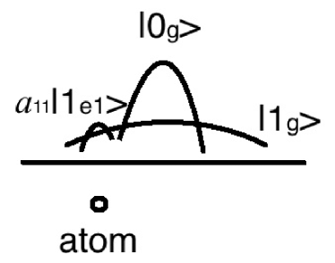
We are in trouble here for the following reasons. The electron states are rather different from as shown in Fig. 2. If expressed as wavefunctions, for example, the state is a diverging Gaussian beam as discussed in Sec. B. On the other hand, recall that the inelastically scattered electron wave generates the diffraction pattern consistent with equation (26) and corresponds to the wavefunction (28), if a plane incident wave is employed. Because of the linearity of quantum mechanics, the wavefunction corresponding to the state equals the product of the Gaussian incident wavefunction and the equation (28). First, such a product may be vanishing if the overlap between the Gaussian envelope and the function (28) is small. In this case, only one term of equation (31) survives and we get amplitude imbarance, or an amplitude error. Second, the phase compensation step described in Sec. A may fail because the optical path length difference is no longer the difference of distances between the detection pixel and the two regions and respectively. Rather, this quantity now involves the modified two regions because the form of is localized at around the scattering atom and is different from . Since we do not know the exact position of the inelastically scattering atom, we cannot compensate for this modification when performing the phase compensation step. Hence, we have problems in terms of both the amplitude and phase.
Since the inner-shell excitations are problematic for the above reasons, we have used the SIGMAK3 and SIGMAL3 programs [66] to evaluate the total K-shell and L-shell cross sections for electrons for the elements C, N, O, and S. (Hydrogen does not have an inner shell.) We combined the result with data presented in Appendix B, which can easily be translated to atomic number density-per-area data for a typical -thick biological specimen. We find that the probability for a single incident electron to cause K-shell or L-shell ionization in such -thick specimen is . This figure is small enough to perform entanglement assisted electron microscopy to our advantage.
2 Delocalized inelastic scattering
The most dominant outer-shell excitations are usually plasmons and here we focus on inelastic scattering by plasmons. Let us first develop a simple but admittedly inaccurate model to grasp essential physics involved. The purpose of doing so is not to estimate quantities we want to know, but to make a connection between the localized case mentioned above to the case of delocalized scattering involving plasmons.
We are interested in specimens consisting of biological molecules embedded in vitreous ice. Clearly, it is not adequate to model such an insulating system by free electrons in a box, as done in studies of plasmons in metals. Without further justifications, let us accept that essential physics of such an insulating system is captured by a set of 1-dimensional harmonic oscillators, which are arranged on a line with a constant interval . (The actual specimen is more like 2-dimensional, but we can oversimplify as long as the purpose is only to grasp essential physics.) Each harmonic oscillator models an atom with a single oscillating valence electron and the immobile rest. Assume that all neighboring two electrons interact as if these are connected by a mechanical spring. This assumption is hard to justify, but for the sake of simplicity we proceed. Then the model is similar to the 1-dimensional model for phonons. The hamiltonian is
| (32) |
where and are the momentum and position of the electron at the -th site, is the electron mass, and are ’spring constants’ of interaction between the -th electron and the neighboring -th electron; and interaction between the -th electron and its ion core, respectively. The last term in the curly bracket in equation (32) is the only difference from the phonon model. We apply the periodic boundary condition, i.e., . Let the plasmon coordinate and momentum operators be
| (33) |
where , . (We use notations that are used in other part of this paper, since there is no danger of confusion.) Following the standard procedure, we have
| (34) |
where
| (35) |
Though the model is crude, this reproduces the usual plasmon dispersion relation as . The standard method of quantization for phonons carries over to the case of plasmons, for which the creation operator is
| (36) |
Now, consider the weak coupling limit . The creation operator for the individual ’bare’ harmonic oscillator at the -th site is
| (37) |
where the bare oscillation frequency is given by . When , or in other words at the large wavelength limit, we have . In this case, combining some of the above relations, we obtain
| (38) |
What equation (38) states is the following. An excitation of a plasmon is equivalent to the superposition of excitations of each scattering atom, with an additional phase factor that corresponds to the phase of the plasmon wave at least in the initial stage of time evolution. Although our model is crude, we will henceforth assume that the preceding statement is robust so that it may be applied to real situations with reasonable degree of validity. From experiments we know that inelastic scattering is associated with a small scattering angle that corresponds to delocalization and long wave length plasmons. Thus, unlike the case of inner-shell electron excitations, when one atom is excited in an inelastic scattering process generating a plasmon, the state must be superposed with other states, in each of which another atom, i.e. one of the surrounding atoms, is excited.
In order to see how an excitation of a plasmon affects the measurement, we consider scattering of a plane wave. This suffices because, first, we can separately consider two terms of the whole wavefunction, containing respectively the CPB state and , and later add the results. Second, all possible incident electron waves, including the diverging spherical wave, can be expanded as a sum of plane waves. We now consider all atoms that contribute their valence electron to form plasmons. For definiteness, let the number of these atoms be . We label them with an integer (changing the meaning of somewhat) and, for simplicity, we consider only the ground state and the first excited state for each of them. Let the position of the -th atom be . Let the incident plane wave be . Since there are many quantum entities, we will generally omit the tensor product symbol . The state before inelastic scattering is
| (39) |
We confine ourselves to the case of single plasmon generation and we neglect terms with two or more atoms excited. A few definitions follow. Let denote the electron state after interacting with the -th atom, without exciting the atom’s electron. (One may view this state as a superposition of the transmitted wave and elastically scattered wave.) We let the state represent the electron state after exciting the atom. Then, after inelastic scattering, the state becomes
| (40) |
where are probability amplitudes to reach the states . (For simplicity we assume that are independent of . This may not be justified, but it will be found later that this will not affect our conclusion.) For brevity, we define some of the state of the whole specimen atoms
| (41) |
and also define an electron state . In terms of these, equation (40) is rewritten as
| (42) |
The first term corresponds to elastic scattering, with the specimen left without excitation. Now, according to the argument in the last paragraph, the state of a plasmon with wave vector is expressed as
| (43) |
Although the atoms are not regularly placed, by analogy with the Fourier transform we write
| (44) |
Hence we have
| (45) |
Therefore, if we observe the plasmon in the state (though this ’observation’ only models the decoherence process and we do not obtain the outcome of such an ’observation’ in practice), the electron wave is left in the state
| (46) |
This is a superposition of electron waves inelastically scattered at each atoms, with a phase factor depending on the position on the specimen. If there are sufficiently many atoms, more-or-less uniformly distributed, then equation (46) describes nothing but a tilted plane wave, whose wave vector is slightly changed by emitting a plasmon. This agrees with the standard picture of momentum conservation.
At this point we make a few remarks. First, if the amplitude depends on (for example, because depends on atomic number Z), then we may divide the atoms into classes with the same values. As long as the number of atoms in each class is sufficiently large to retain the above Fourier-transform-like property, the conclusion stands. Conversely, one may simply neglect a class that comprises too few of atoms. Second, one may argue that ’observing’ the plasmon with respect to the measurement basis is rather arbitrary and the use of other basis should be analyzed as well. However, there are no interactions between the electron and the specimen after scattering, and statistical measurement outcomes regarding the scattered electron should not depend on how the plasmon state is ’measured’. (Of course, being entangled to each other, the ’measurement outcomes’ on the electron and the plasmon are correlated.) In addition, we will find the use of the basis highly convenient. Third, as far as there are many atoms in the regions and , all these atoms contribute to the scattered wave amplitude and there will not be much variation of the wave amplitude within the respective regions. Hence, unlike the case of inner-shell electron excitations, we do not expect to have much amplitude error. Fourth, we may say that the effect of having plasmon scattering is equivalent to have a thin ’wedge prism’ right next to the specimen. Every time inelastic scattering occurs, the rotation angle of the ’wedge prism’ around the optical axis is completely random. The ’angle between two planes of the wedge’ is also random but generally obeys the formula (26) that specifies the distribution of inelastic scattering angles. When viewed in this way, it should be clear that no matter what incident beam we use, be it focused Gaussian or diverging Gaussian, the effect of plasmon generation is to tilt the exit wave from the specimen by an angle proportional to the size of the plasmon wave vector.
The phase error due to plasmon excitations is more problematic than the amplitude error. The mechanism for the error is that the scattered electron wave is tilted by the aforementioned ’wedge prism’ and hence the phase compensation step (See Sec. A) cannot be done accurately. Let us first roughly estimate the extent of such an error. The formula (26) is in a sense misleading because the average scattering angle is much larger than the ’characteristic angle’ . In fact, the mean scattering angle does not even exist for the Lorentzian distribution unless we introduce a cutoff angle , above which there is no scattering. The angle for the Bethe-ridge is usually taken as a cutoff, which in our case is . Let us compute the fraction of inelastically scattered electrons with the scattering angle less than . This is given by
| (47) |
Approximating , we get
| (48) |
From this, one may compute, for example, that half of all inelastically scattered electrons have the scattering angle larger than . In other words, this is the median scattering angle and it is much larger than . A similar calculation yields the mean scattering angle . These numbers suggests that the probability distribution is quite unusual due to the long tail.
We estimate the phase error due to failure in performing the phase compensation step. First, consider the case of focused incident beam (Sec. A). As in Appendix A, we take -axis to be the optical axis. Let the regions and be separated by a distance along -axis. Let the pixel, in which the scattered electron is detected, be A. Let the distance between the point A and the central points of the specimen regions and be and respectively. Then, the optical path length difference is . The detection pixel is placed on the plane without loss of generality. The scattering angle is . Simple geometrical consideration then yields . Now, suppose that a plasmon is generated upon scattering, to the direction of -axis. The path length difference is modified because of the presence of aforementioned ’wedge prism’, to be where is the angle of the ’wedge prism’, which actually is the inelastic scattering angle. The error in estimating the optical path length difference in the phase compensation step would therefore be , if we take mean angle error for plasmon scatterings as the angle of the ’wedge prism’ . The error, in terms of phase angle, is unacceptable , where is the wave number of electrons. In addition to the error due to the ’speckle pattern’ problem mentioned in Sec. A, this constitutes another reason why the focused-incident-beam configuration is not desirable.
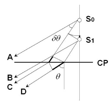
Let us turn to the case of diverging incident beam, described in Sec. B. Figure 3 shows that the Gaussian electron beam focused at either or above the specimen central plane CP. The focal points corresponding to the regions and are labeled with the same symbol. The distance between these focal points is denoted as . Let be the scattering angle and let be the deflection angle due to plasmon generation. The plasmon scattering occurs at CP in the figure, but exactly where the scattering occurs does not matter, as the reader will see shortly. We assume that the plasmon momentum vector is parallel to -axis, which is the worst case. The four ’optical rays’ A, B, C and D go to the same direction under CP. The rays A and B represents optical paths taken by electrons that are not inelastically scattered, whereas the rays C and D shows optical paths associated with plasmon generation. In computing the optical path length difference, we always make the approximation for any angle. Then, computation of the optical path length difference is a matter of simple exercise in geometry. The optical path length difference in the absence of inelastic scattering, between rays A and B is . On the other hand, the three thick portions of rays in Fig. 3 contributes the path length difference between rays C and D, which turns out to be . Thus, the change of the optical path length difference due to the plasmon scattering is . The magnitudes of is about the median inelastic scattering angle or the mean , depending on how one defines the ’typical’ scattering angle. The error in terms of phase, then, is or . The latter is not small and requires further investigation.
In order to resolve the question of how plasmon scattering affects the measurement, we resort to numerical simulation. We employ electrons in a k-electron process. We estimate the frequency of the plasmon scattering as follows. At near the end of Sec. A, it was found that the probability of elastic scattering for electrons is for a thick specimen. On the other hand, generally inelastic scattering is considered to occur twice as frequent as elastic scattering as mentioned earlier. Hence we take a value of as inelastic scattering probability. We will ignore the failure due to high-angle elastic scattering (probability as computed earlier) and inner-core electron excitations (probability ), as these are sufficiently rare. Indeed, when these probabilities are added we have . A simple consideration shows that the k-electron process fails with a probability . A waste of electron dose is acceptable.
Following Ref. [42], we consider cryoelectron microscopy of the ribosome molecule. However, unlike Ref. [42] we consider electrons. Otherwise the method of simulation is the same as Ref. [42], except that we now consider inelastic scattering that occurs of times at random. When it is decided in our simulation program that inelastic scattering happened, the phase error is computed as follows. First, a uniform random number in the interval is generated. Then we use equation (48) by letting and compute . Clearly, obeys the statistical distribution governing inelastic scattering angle. On the other hand, suppose that the plasmon wave vector is proportional to , where are unit vectors parallel to axes, respectively. Geometrical consideration shows that the phase error in angle is , where is a random number drawn uniformly from the interval . Since this error adds to the phase we want to measure during a k-electron process, equation (7) is now modified as
| (49) |
where represents the total error accumulated in the k-electron process. It is the sum of all individual error occurred during the k-electron process. More precisely, if inelastic scattering happened in a k-electron process, then there are independent random variables , that are summed up to produce .
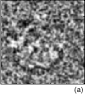
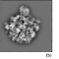
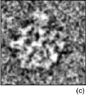
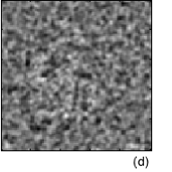
Figure 4 shows the simulation result. Each image consists of pixels and the size of the image is . The size of Gaussian beams to the regions are respectively and at the entrance surface of the specimen. As mentioned in Sec. B, there is a significant beam spread in the specimen but we did not take the spread into account in the simulation, which has been performed as if there were no such spread [67]. The electron dose is . Perfect detector efficiency and the CPB readout efficiency is assumed. The ’raw’ image is smoothed with a Gaussian filter with a standard deviation for better visibility. A simulated image of entanglement-assisted electron microscopy, which takes errors due to inelastic scattering into account, is shown in Fig. 4 (a). For the sake of comparison, a ’Laplacian-filtered’ [69] phase shift map of the ribosome, from a X-ray study [68], is shown in Fig. 4 (b); the hypothetical case where inelastic scattering is absent, but otherwise identical situation , is shown in Fig. 4 (c); and an image for the ’conventional’ case, where perfect in-focus phase contrast microscopy is employed with the same dose, also ’Laplacian-filtered’, is shown in Fig. 4 (d).
V Conclusion
We evaluated measurement errors in entanglement-assisted electron microscopy, due both to elastic and inelastic scattering processes at the specimen. Despite remaining subtleties such as processing of data obtained by the significantly divergent electron beam, overall we have found no evidence that entanglement-assisted electron microscopy is not viable for some fundamental physical reasons related to electron scattering processes. There are several lessons learned along the way. First, despite the fact that lossy processes are often emphasized as the sole fundamental limit in the quantum metrology literature, elastic scattering processes present a limit just as fundamental in the present case. The reason is that the elastic scattering signal sometimes contains information that we do not need, because the information is about too high resolution features of the specimen that cannot be fully obtained anyway. This leads to an error which cannot be controlled nor corrected, but it has been computed to be sufficiently small. Second, besides the inner-shell excitation processes associated with a sufficiently small cross sections, inelastic scattering processes involve generation of plasmons. The excitation of a plasmon results in bending of the probe electron wave, which in turn entails phase error because the phase compensation step of the entanglement-assisted electron microscopy cannot be carried out precisely. We found that the magnitude of such an error is acceptable. Rather remarkably, how the two probe electron states (that are entangled to the two CPB states) are geometrically arranged is found to be important in order to reduce this type of error.
Many issues are left for future investigations. For example, the most suitable energy of the primary electron beam, which presumably depends on the specimen thickness, has not been fully understood, although the present author feels that higher energy is better, unless knock-on damage comes in to play a significant role. Furthermore, errors associated with the electron reflection process at the electron mirror equipped with the CPB, or errors associated with the CPB control processes, have largely been unexplored.
Acknowledgments
I thank Umpei Miyamoto for his help with TEX. This research was supported in part by the JSPS “Kakenhi” Grant (#25390083).
APPENDIX A: EXPRESSIONS OF THE ELASTIC SCATTERING AMPLITUDE
Here we derive equations (9), (11) and (15) appeared in Sec. III and clarify what approximations are involved in the derivation. Let us first deal with the case of Sec. A. The incident Gaussian wave is a superposition of many plane waves. For a constituent plane incident wave , after elastic scatterings we have, in the far field
| (50) |
where is the ’wave number vector after the scattering’, whose primary purpose is to point at the point P, where we wish to compute the value of the wavefunction, and is the angle between the vectors and . We are dealing with elastic scattering and , at least to a good approximation. We ignore the imaginary part of , as is done in the Born approximation though this cannot be entirely correct because of the Optical Theorem. As usual, when appearing in the denominator in eq. (50) is much greater than all relevant , may be approximated to be . This is a representative distance between the whole specimen and the point P. Let the component of the vector be respectively , which we write . We want the incident beam to be Gaussian with the waist size and the above plane wave solutions are superposed as
| (51) |
The factor is introduced solely to simplify some of later expressions and keep them dimensionless. The diffraction-limited waist of the Gaussian beam is on the specimen. At , the incident beam part is
| (52) |
Note that the component of the -vector is in above equations and the limits of integrations in equation (52) are approximated as positive and negative infinities. Far from the specimen, the transmitted Gaussian wave has the known form
| (53) |
This, when , is equation (9) of the main text.
Next, we consider the scattered part of the wave amplitude
| (54) |
Note that, if the phase factor were identically , which it is not, the integration in the square brackets in equation (54) would represent, up to a constant multiplicative factor, something akin to, but not identical with, Gaussian smoothing of .
To evaluate the phase factor , we write it as . Let us first consider the exit wave, and focus on a single pixel of the detector. Since the pixel is on a diffraction plane, is independent of . In other words, it is independent of the place of the atom under consideration. Without loss of generality, we assume that the pixel under consideration is on the plane. Let the angle between -axis and be . Then the detector pixel is located at , where is much greater than any . Writing , we have
| (55) |
Let us now turn to the incident wave and write . It is clear that the angle between and -axis is , , and hence when these angles are small. Putting them together, the phase factor equals
In order to further approximate, we check some numbers here. Because of the waist size (since we want a diameter), and are at most , while is up to the specimen thickness . From the theory of Gaussian beams we know that the wave convergence half-angle is , where the wave number is for electrons. This makes (and the ’focal depth’, or the Rayleigh range , is ). Noting that is at most of the order , the phase factor in the square bracket in equation (57) may be approximated as . On the other hand, the meaningful magnitude of should roughly be given by the “characteristic angle of elastic scattering” , where is the screening radius of the atom and is given by , where and are the Bohr radius and the atomic number, respectively [57]. For most relevant elements (See Appendix B) and we have and and in the case of hydrogen this is even smaller. These numbers allow us to further approximate equation (57) to yield
| (58) |
This approximation should be understood as, for example, keeping only the phase shift associated with atoms with large values. (We have the phase factor for atoms with smaller values also, but that may be less significant than the neglected .) Furthermore, since the presence of the factor implies that the integration, in terms of the angle , is over a narrow range of the order . This is fairly smaller than the ’spread’ of the function , that is , when plotted with respect to . These facts allow us to approximate equation (58) to obtain
| (59) |
The integral is the two-dimensional Fourier transform of a Gaussian function and we get
| (60) |
This is equation (11) of the main text.
We now turn to the second case described in Sec. B. The above discussion up to equation (57) holds also here. We keep the Gaussian beam waist at , but the atoms in the specimen are no longer at but at near that is or , depending on whether the region under consideration is or . The coordinate of the -th atom is now , where is at most . Equation (57) is then rewritten as
| (61) |
Here, we need to consider the range of up to , which is the sum of the incident beam divergence and the characteristic angle . The coordinates are at most and are at most . Hence equation (61) is approximated as
| (62) |
though the approximation is not good. Consider the integral in the square bracket. The phase factor has the associated phase angle up to . In our case and , thus one may say that the phase angle rotates fairly rapidly. Hence the value of matters only at around , where no first-order phase oscillation occurs. Since and , we have to the first order in . Hence, we further simplify equation (62) as
| (63) |
We must note, however, that this approximation is only barely justifiable because the phase factor is fairly constant in an angular range , where is the wavelength of electrons. Taking , we have , which actually is comparable to the characteristic angle associated with the scattering amplitude . Due to the lack of simple and good analytical alternatives we proceed. The integral is a convolution of two functions that equals
| (64) |
It may be verified that and we define . (The parameter has a physical meaning of the ratio between the waist size of the incident beam and the incident beam ’radius’ at the distance from the waist. Alternatively, , where is the Rayleigh range.) Hence, equation (63) approximately equals
| (65) |
This is equation (15) in the main text.
APPENDIX B: ATOMIC NUMBER DENSITIES IN A TYPICAL BIOLOGICAL SPECIMEN
We consider a frozen, hydrated speimen that is typical in biological cryoelectron microscopy and compute the associated atomic number densities for the elements H, C, N, O, and S. The water content may vary considerably from specimen to specimen. However, for simplicity we take values of 76% water and 24% “dry weight” as typical composition, which has been reported as the composition of “sediments obtained by predetermined dilution of pellets harvested by centrifugation” of yeast suspension [70]. The component which contributes to the dry weight may in general contain things other than protein. However, again for simplicity, we assume that the component consists solely of protein. Then, given the known density of low density amorphous (LDA) ice 0.94 g/cc [71], the standard value of protein density 1.35 g/cc (But see also [72]), and the reported amino acid frequencies in representative proteins [73], the representative atomic number densities for the elements H, C, N, O, and S may be computed. The results are shown in Table 1.
| Element | H | C | N | O | S |
|---|---|---|---|---|---|
| Number Density [atoms/] | 62 | 6.4 | 1.8 | 28 | 0.067 |
References
- [1] R. M. Glaeser and K. A. Taylor, J. Microsc. 112, 127 (1978).
- [2] M. Adrian, J. Dubochet, . Lepault and A. W. McDwall, Nature (London) 308, 32 (1984).
- [3] At first glance, biological specimens may seem to be weak amplitude objects rather than weak phase objects because in a typical frozen hydrated biological specimen, the inelastic scattering cross section is about two times greater than the elastic counterpart [7]. However, when phase contrast imaging is used, the phase shift of the electron wave, which directly translate to image contrast, is proportional to , whereas , representing intensity loss, contributes linearly to the contrast. The former contribution to the contrast is generally larger than the latter.
- [4] R. Henderson, Q. Rev. Biophys. 28, 171 (1995).R. M. Glaeser and K. A. Taylor, J. Microsc. 112, 127 (1978).
- [5] C. A. Diebolder, A. J. Koster, and R. I. Koning, J. Microsc. 248, 1 (2012).
- [6] V. Lucic, F. Forster, and W. Baumeister, Annu. Rev. Biochem. 74, 833 (2005).
- [7] R. M. Glaeser, K. Downing, D. DeRosier, W. Chiu and J. Frank, Electron Crystallography of Biological Macromolecules (Oxford University Press, New York, 2007).
- [8] J. Frank, Ultramicroscopy 1, 159 (1975).
- [9] X. Yu, L. Jin, and Z. H. Zhou, Nature (London) 453, 415 (2008).
- [10] R. Danev and K. Nagayama, Ultramicroscopy 88, 243 (2001).
- [11] E. Majorovits, B. Barton, K. Schultheiss, F. Perez-Willard, D. Gerthsen, and R. R. Schroder, Ultramicroscopy 107, 213 (2007).
- [12] R. Cambie, K. H. Downing, D. Typke, R. M. Glaeser, and J. Jin, Ultramicroscopy 107, 329 (2007).
- [13] R. F. Egerton, Rep. Prog. Phys. 72, 016502 (2009).
- [14] T. Sasaki, H. Sawada, F. Hosokawa, Y. Kohno, T. Tomita, T. Kaneyama, Y. Kondo, K. Kimoto, Y. Sato, and K. Suenaga, J. Electron Microsc. 59, S7 (2010).
- [15] N. Dellby, N. J. Bacon, P. Hrncirik, M. F. Murfitt, G. S. Skone, Z. S. Szhlagyi, and O. L. Krivanek, Eur. Phys. J. Appl. Phys. 54, 33505 (2011).
- [16] U. Kaiser, J. Biskupek, J. C. Meyer, J. Leschner, L. Lechner, H. Rose, M. Stoger-Pollach, A. N. Khlobystov, P. Hartel, H. Muller, M. Haider, S. Eyhusen, and G. Benner, Ultramicroscopy 111, 1239 (2011).
- [17] For example, it is reasonable to estimate the inelastic mean free path of 20 kV electrons to be in the range of a few tens of nm, if we take the following three facts into account: 1) Data presented in M. P. Seah and W. A. Dench, Surf. Interface Anal. 1, 2 (1979) show a trend at lower voltages. 2) The mean free path is 160 nm in vitreous ice (B. Feja and U. Aebi, J. Microsc. 193, 15 (1999) and references therein). 3) The mean free path in frozen protein is somewhat shorter than the vitreous ice case, as described in Chap 15, Ref. [7]. Moreover, a short elastic mean free path would also be problematic, as multiple scatterings would make interpretation of images much more difficult.
- [18] Y. Fujiyoshi and N. Uyeda, Ultramicroscopy 7, 189 (1981).
- [19] M. Koshino, T. Tanaka, N. Solin, K. Suenaga, H. Isobe, and E. Nakamura, Science 316, 853 (2007).
- [20] V. Giovannetti, S. Lloyd, L. Maccone, Nature Photonics 5, 222 (2011).
- [21] C. W. Helstrom, Quantum Detection and Estimation Theory (Academic, New York, 1976).
- [22] H. P. Yuen, Phys. Rev. A 13, 2226 (1976); C. M. Caves, Phys. Rev. D 23, 1693 (1981).
- [23] B. Yurke, Phys. Rev. Lett. 56, 1515 (1985).
- [24] J. J. Bollinger et al., Phys. Rev. A 54, R4649 (1996).
- [25] A. N. Boto et al., Phys. Rev. Lett. 85, 2733 (2000).
- [26] V. Giovannetti, S. Lloyd, L. Maccone, Phys. Rev. Lett. 96, 010401 (2006).
- [27] M. Zwierz, C. A. Perez-Delgado, and Pieter Kok, Phys. Rev. A 85, 042112 (2012).
- [28] A. Luis, Phys. Lett. A 329, 8 (2004); J. Beltran and A. Luis, Phys. Rev. A 72, 045801 (2005); S. M. Roy and S. L. Braunstein, Phys. Rev. Lett. 100, 220501 (2008).
- [29] M. Napolitano, M. Koschorreck, B. Dubost, N. Behbood, R. J. Sewell, and M. W. Mitchell, Nature 471, 486 (2011).
- [30] R. Demkowicz-Dobrzanski, J. Kolodynski, and Madalin Guta, Nat. Commun. 3, 1063 (2012).
- [31] L. Maccone and G. De Cillis, Phys. Rev. A 79, 023812 (2009).
- [32] R. Demkowicz-Dobrzanski et al., Phys. Rev. A 80, 013825 (2009).
- [33] C. Vitelli, N. Spagnolo, L. Toffoli, F. Sciarrino, and F. De Martini, Phys. Rev. Lett. 105, 113602 (2010).
- [34] J. Kolodynski and R. Demkowicz-Dobrzanski, Phys. Rev. A 82, 053804 (2010).
- [35] P. C. Humphreys, M. Barbieri, A. Datta, and I. A. Walmsley, Phys. Rev. Lett. 111, 070403 (2013).
- [36] A. Luis, Phys. Rev. A 65, 025802 (2002).
- [37] H. Okamoto, T. Latychevskaia, and H.-W. Fink, Appl. Phys. Lett. 88, 164103 (2006).
- [38] H. Okamoto, Appl. Phys. Lett. 92, 063901 (2008).
- [39] R. M. Glaeser, Phys. Today 61, 48 (2008).
- [40] W. P. Putnam and M. F. Yanik, Phys. Rev. A 80, 040902(R) (2009).
- [41] H. Okamoto, Phys. Rev. A 81, 043807 (2010).
- [42] H. Okamoto, Phys. Rev. A 85, 043810 (2012).
- [43] A. Elitzur and L. Vaidman, Found. Phys. 23, 987 (1993).
- [44] P. Kwiat, H. Weinfurter, T. Herzog, A. Zeilinger, and M. A. Kasevich, Phys. Rev. Lett. 74, 4763 (1995).
- [45] G. Mitchison, S. Massar, and S. Pironio, Phys. Rev. A 65, 022110 (2002).
- [46] In contrast to Ref. [42], here we use the symbol instead of for the quantum phase angle, in order not to be confused with the scattering angle .
- [47] M. Buttiker, Phys. Rev. B 36, 3548 (1987); P. Lafarge, P. Joyez, D. Esteve, C. Urbina, and M. H. Devoret, Nature (London) 365, 422 (1993); Y. Nakamura, Yu. A. Peshkin, and J. S. Tsai, Nature (London) 398, 786 (1999).
- [48] A. Blais, R.-S. Huang, A. Wallraff, S. M. Girvin, and R. J. Schoelkopf, Phys. Rev. A 69, 062320 (2004); A. Wallraff, D. I. Schuster, A. Blais, L. Frunzio, J. Majer, M. H. Devoret, S. M. Girvin, and R. J. Schoelkopf, Phys. Rev. Lett. 95, 060501 (2005).
- [49] V. A. Lobastov, R. Srinvasan, and A. H. Zewail, Proc. Natil. Acad. Sci. USA 102, 7069 (2005); M. Merano, S. Collin, P. Renucci, M. Gatri, S. Sonderegger, A. Crottini, J. D. Ganiere, and B. Deveaud, Rev. Sci. Instrum. 76, 085108 (2005).
- [50] T. Nagao, Y. Iizuka, M. Umeuchi, T. Shimazaki, M. Nakajima, and C. Oshima, Rev. Sci. Instrum. 65, 515 (1994).
- [51] J. Yang, K. Kan, N. Naruse, T. Kondoh, Y. Yoshida, K. Tanimura, T. Takatomi, and J. Urakawa, in Proceedings of the 9th Annual Meeting of Particle Accelerator Society of Japan, 2012 (unpublished) p. 282.
- [52] R. Weber, E. Tanabe, and Y. Nagatani, in Proceedings of the 9th Annual Meeting of Particle Accelerator Society of Japan, 2012 (unpublished) p. 1325.
- [53] B. C. Sanders, Phys. Rev. A 40, 2417 (1989).
- [54] A. Rother and K. Scheerschmidt, Ultramicroscopy 109, 154 (2009).
- [55] A. Jablonski, F. Salvat, and C. J. Powell, NIST Electron Elastic Scattering Cross-Section Database - Version 3.2, National Institute of Standards and Technology, Gaithersburg, MD (2010).
- [56] R. Enri, M. D. Rossell, C. Kisielowski, and U. Dahmen, Phys. Rev. Lett. 201, 096101 (2009).
- [57] R. F. Egerton, Electron Energy-Loss Spectroscopy in the Electron Microscope, 3rd Ed. (Springer, 2011).
- [58] K. Kimoto and Y. Matsui, Ultramicroscopy 96, 335 (2003) and references therein.
- [59] R. W. Ditchfield, D. T. Grubb, and M. J. Whelan, Philos. Mag. 27, 1267 (1973).
- [60] J. P. Langmore and M. F. Smith, Ultramicroscopy 46, 349 (1992).
- [61] R. Leapman and S. Sun, Ultramicroscopy 59, 71 (1995).
- [62] J. Wall, M. Isaacson, and J. Langmore, Optik 39, 359 (1974).
- [63] R. F. Egerton, S. Lazar, and M Libera, Micron 43, 2 (2012).
- [64] R. F. Egerton, S. Lazar, and M. Libera, Micron 43, 2 (2012).
- [65] D. A. Muller and J. Silcox, Ultramicroscopy 59, 195 (1995).
- [66] R. F. Egerton, freely downloadable MATLAB programs available at: www.tem-eels.ca
- [67] The present author feels that appropriate data processing, which is not dissimilar to computational tomography, would help solving this problem. However, this has not been demonstrated as of now.
- [68] N. Ban, P. Nissen, J. Hansen, P. B. Moore, and T. A. Steiz, Science 289, 905 (2000).
- [69] The ’Laplacian filter’ [42] computes the difference of the following two data: The first data is the result of applying a Gaussian filter with the ’standard deviation ’ to the unprocessed data, while the second is the same except that the standard deviation is . It was done on figures (b) and (d) to extract high resolution components only, in order to make a comparison with figures 4 (a) and (c).
- [70] J. L. Uribelarrea, S. Pacaud, and G. Goma, Biotech. Lett. 7, 75 (1985).
- [71] D. T. Bowron, J. L. Finney, A. Hallbrucker, I. Kohl, T. Loerting, E. Mayer, and A. K. Soper, J. Chem. Phys. 125, 194502 (2006); T. Loerting, K. Winkel, M. Seidl, M. Bauer, C. Mitterdorfer, P. H. Handle, C. G. Salzmann, E. Mayer, J. L. Finney, and D. T. Bowron, Phys. Chem. Chem. Phys. 13, 8783 (2011).
- [72] H. Fischer, I. Polikarpov, and A. F. Craievich, Protein Sci. 13, 2825 (2004).
- [73] J. L. King and T. H. Jukes, Science 164, 788 (1969).