Phonon Diodes and Transistors from Magneto-acoustics
Abstract
By sculpting the magnetic field applied to magneto-acoustic materials, phonons can be used for information processing. Using a combination of analytic and numerical techniques, we demonstrate designs for diodes (isolators) and transistors that are independent of their conventional, electronic formulation. We analyze the experimental feasibility of these systems, including the sensitivity of the circuits to likely systematic and random errors.
pacs:
85.70.Ec, 63.20.kk, 72.55.+s, 43.25.+yHeat is ubiquitous. It accompanies almost any form of energy loss in real systems, but is one of the most difficult phenomena to control precisely. The most successful utilizations of heat (e.g. heat engines and heat pumps) essentially treat it as a homogenous current. However, consider crystals, where heat is often transported by electrons, photons, and phonons. There exist impressive arrays of devices for controlling both electrons and photons (down to specific modes and locations), but no equivalent toolkit for phonons. Perhaps the starkest example of this is computing, where strict control of a signal’s state is compulsory and commonplace. Recent efforts have sought to extend this degree of control to phonons, to realize devices like diodes, transistors, logic, and memory Phononics ; Phn Logic ; Phn Diode ; Phn Transistor ; Phn Mem . Throughout this process the assumption that all computers should be the strict analog of electronic computers has been implicit. Since information in electronics is scalar (high or low voltage = 1 or 0), it has been assumed that information from phonons would be encoded in temperature (hot or cold = 1 or 0). Similarly, since electronics uses pn junctions for constructing circuits, interface effects have been considered for phonon diodes. Hence, research has thus far focused on nano-structures CNT Rect ; VO Rect or 1D materials Phononics ; Phn Logic ; Phn Diode ; Therm Rect , where interface effects are strong, but fabrication was difficult.
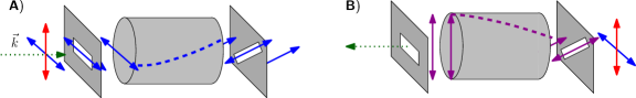
Abandoning the assumption that phononic and electronic computing are strictly analogous presents a host of new opportunities. Here, we make an analogy to optical computing. We encode information in the polarization of a phonon current (transverse vertical or horizontal = 1 or 0). Our operators therefore modify some generic elliptic polarization, i.e. gyrators (which rotate the polarization angle) and polarizers (which project the polarization) from which we can construct diodes and transistors. The relationship between devices used in electronics, optics, and phononics and the abstract logic elements is shown in Figure 1 111In optics isolators are essentially diodes Pht Isolator .. To make these, we require systems that break time-reversal, rather than reflection, symmetry that is, we require a magnetic field. For the magnetic field to have a measurable effect upon the phonon current, we focus on magneto-acoustic (MA) materials. These materials were first described by Kittel, who noted that they could be used to create “gyrators, isolators [diodes], and other nonreciprocal acoustic elements” Kittel , but subsequent research on MA focused on other applications (e.g. acoustic control of magnetization) GG Book ; AFM Th ; TGG Exp ; Luthi Book ; Magnons . MA coupling is a bulk effect found in commercially available materials, so fabrication is easier compared to the nano-structures of the electronic analogy.

In this article, we employ a combination of analytic and numerical methods to demonstrate that phononic logic elements (diodes and transistors) can be designed outside of an electronic computing paradigm. Our results confirm that MA polarizers and gyrators, when combined with a means of generating and measuring phonon currents, are sufficient to realize logic elements. Further, we show how present experimental techniques are likely sufficient to actualize logic elements that are reliably insensitive to errors. Taken together, these results reveal the potential for an under-explored class of phonon logic gates.
The goal of this work is to explore the feasibility of frequency-dependent phonon computing. In order to tackle this, knowledge of the phonon dispersion’s dependence on fixed (e.g. length) and tunable (e.g. magnetic field) parameters is necessary. Hence, we begin with the dispersion relation for two special geometries.
When the magnetic field is oriented along the length of the MA (, where is the applied field and the phonon wavevector), we have the circular birefringence (acoustic Faraday effect (AFE)) necessary for a gyrator GG Book . The dispersion relation is:
| (1) |
where are the right and left circularly polarized wavevectors (at fixed frequency ), the natural length scale ( where the shortest relevant lifetime, typically the magnon lifetime, the stiffness constant, and the density), the dimensionless frequency , the dimensionless field strength ( is the gyroscopic ratio), and the dimensionless coupling constant ( is the MA constant and the saturation magnetization of the MA, assuming a net ferromagnetic moment exists). Conversely, when the magnetic field is oriented perpedicular to the length of the MA (), we have linear birefringence (Cotton-Mouton effect), necessary for a polarizer GG Book . The dispersion relation for the mode polarized along the magnetic field is:
| (2) |
whereas the mode polarized perpendicular to the magnetic field is unaffected by the magnetic field (). In both cases, there will be both real and imaginary components to the dispersion, corresponding to birefringence and dichroism 222Dichroism can have any sign in MA, as energy can be added or extracted from the magnetic field.
In optics, diodes are constructed by sandwiching a gyrator between two linear polarizers (oriented by with respect to each other (see Fig. 2)) Pht Isolator . A signal entering in the forward mode, passes through the first polarizer, acquires a rotated polarization from the gyrator, and emerges polarized along the second polarizer. Conversely, a signal in the reverse direction is polarized and then acquires the same rotation in polarization, emerging orthogonal to the second polarizer. Both polarizers and gyrators can be constructed from MA by tuning the magnetic field. For a diode, one must select magnetic field strengths (at fixed frequency) that yield weak dichroism for the gyrator (even weak circular dichroism can prevent complete destructive interference, as we see below) and strong dichroism for the polarizer.
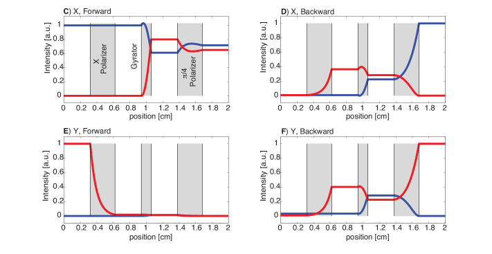
Our independent parameters for designing the gyrators and polarizers are field strength, phonon frequency, and MA length. We assume that the properties of the MA are fixed, taking values from representative experiments EXP . The Phonon frequency is selected to be 10 GHz (slightly larger than in EXP ). is then calculated for each dispersion and used to select reasonable magnetic fields that give desirable ratios of birefringe to dichroism (0.01T for the polarizers and 0.1T for the gyrator). Lastly, lengths are selected such that the gyration ( ) and filtering () are effective. The resulting circuit is then modeled by numerically evaluating the phase acquired by the phonon current at each stage. The results are plotted in Figure 2, where we find the circuit successfully blocks ( loss of intensity) all signals except the desired polarization and direction. Because the AFE’s solutions have opposite signs in their imaginary components, the amplification found in the forward mode is expected (the polarizers suppress it in the reverse).
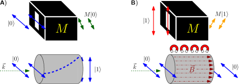
Turning to the transistor, we require a more complicated approach. Firstly our transistor requires a measurement apparatus. This type of measurement remains difficult, but we show a heuristic approach in Fig. 3. While there may be more efficient experimental realizations, the form presented here benefits from its conceptual simplicity. The different stages of detection and transduction (piezoelectric), rectification (electronic diode), amplification (op amp), and application (electronic transistor, electromagnet) are all differentiated and are in principle realizable.

Given a measurement operator, we send a fixed logical 0 signal into a gyrator, and then determine if a magnetic field should be applied by measuring the amplitude of the phonon current for one polarization. If this polarization exceeds some threshold, a magnetic field is supressed (the gyration is strongest as 333The model used here does not include thermal fluctuations reducing the MA’s magnetization at remanence that of saturation. A small, non-zero field is likely prefereable.; remanence magnetization provides the necessary magnetic field to keep the gyrator working). Conversely, when the threshhold is not reached, then a magnetic field will be applied, suppressing the birefringence and partially cancelling the gyration (perfect cancellation requires ). These two operations are summarized in Fig 4A,B.
For the transistor to work as a logic operation, the gyration should be . Using the same process as in the design of the diode (magnetic field of T for off and 0.5T for on), we model the transistor in Figure 4C,D. In doing so we abstract the measurement device, focusing instead on the effect of applying or suppressing a magnetic field.
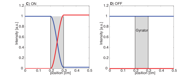
We find that there are imperfections in each operating regime. When the gyrator is off (field applied), the relatively modest size of the field implies a small gyration is still present. Whereas, when the gyrator is on, circular dichroism prevents perfect cancellation of the left and right circularly polarized modes, resulting in a small horizontally polarized remnant. For the specific case of an incoming signal at and the length optimized for , the outgoing polarization angle is limited by
| (3) |
While this can be accounted for by allowing some fuzziness to the range of polarizations that are deemed logical 0 or 1 (indeed, the piezoelectric transduction in Fig 3 is relatively insensitive to the undesired polarization), there is a more stringent limit implied by these errors. Since the undesireable gyrations in the off state will accumulate, there exists a maximum total length of transistors that can be chained in series while maintaining well-separated logic states. This problem can be surmounted in practice by applying a repeater circuit (which maps a noisy input to a desired, less noisy value, as occurs in our transistor design when the signal is sent to the gate, not the source). If we think of each gyrator in a series as tied to a separate gate input, then this also limits the number of independent inputs in a logic operation that can be performed without using a repeater. We can exceed this limit because multiple phonon currents can superimpose, but practical difficulties in distinguishing between different inputs for super-imposed signals make it unlikely that this distinction will do more than double the number of logical inputs. To estimate the practical implications of this limitation, we consider the following encoding. Logical 0 is [0,/5] and logical 1 is [3/10,/2] (other quadrants mapping to the 1st by reflection symmetry). In this case, using our previous independent parameter values, we find that the number of (fixed length) gyrators goes as
| (4) |
where is the maximum number of gyrators and the applied field strength in Tesla. The minimum allowable field strength for the off state is therefore 0.4T. While a similar limit for the on state exists, the insistence on for this regime makes it a weaker constraint on the number of stages and field.
The presence of circular dichroism in the AFE produces a systematic error that limits computational power. In addition to systematic errors, random errors can also corrupt a circuit’s operation (be it diode or transistor). While sufficiently thick polarizers are relatively insensitive to such errors (the damping is exponential), gyrators can be quite sensitive. In general, this sensitivity depends upon frequency and field strength. To assess the sensitivity for an arbitrary case, we use the linearized equation of uncertainty propagation. Expressing the result in fractional uncertainties gives:
| (5) |
This method overestimates the effects of random errors since it does not distinguish between contributions to the real and imaginary parts of the dispersion. To determine the maximum tolerance for a given error, we consider each error acting alone. The results of this calculation are summarized in Table 1. The dramatically worse tolerances for the polarizers in the diode are due to reliance on resonant losses, which constrains . However, the operation of the polarizers is perhaps the least important part of the diode. So long as they produce appreciable losses, their precise magnitude is unimportant. Hence we can more easily accept errors here than other parts of the circuit. Moreover, we can always improve polarizers by increasing their thickness.
| Polarizer | Gyrator | Transistor | |
|---|---|---|---|
| 81.5G | 3.42G | 25.0G | |
| 3.32kHz | 34.2MHz | 49.5MHz | |
| 30.0m | 12.0m | 10.0m |
This trade-off between performance and thickness is a common feature in our circuits. Ergo, it is worth considering some of the problems that might hinder circuit minimization. Here, we considered systems with length scales in the mm-cm range because this possessed the most robust body of experimental literature GG Book ; TGG Exp ; Magnons ; Luthi Book ; YIG Exp ; EXP . However, for practical computers, working with smaller feature sizes is preferable. This has several difficulties for our approach. The most fundamental limit is that, for 10GHz phonons in YIG (as we consider here), the wavelength is about 2.5m. For feature sizes smaller than a wavelength, the assumption that the device can simply be treated as a continuous medium ceases to be applicable and we are forced to treat our devices as defects in a background medium. To exceed this limit, would likely require even higher frequency phonons, where techniques to prepare and measure shear waves are less developed Pico Phn ; Pico Phn2 . Even before we reach this limit, shrinking the system while maintaining the same effect (i.e. ) is a non-trivial demand. For gyrators, in the off-state limit (), the phase acquired is proportional to . Since we don’t care about decreasing the phase acquired, then we can simply allow to decrease without needing to modify any other parameters. In the on-state (), however, the phase is proportional to (for small ). Shrinking therefore requires a concomitant increase in (and only result in an approximate invarience) or a modification of the material used. Finally, for the polarizers, assuming that we’re on-resonance (), then the requirement of phase invariance is quite similar to the active gyrator (although not as strict, since a more effective polarizer is still acceptable). To modify the MA material is therefore likely necessary for miniaturizing our circuits. This could be done in several ways. The most promising modifications of this approach would be to use single molecule magnets, which also show MA properties SMM , or a bulk MA with a reduced speed of sound (exposing the phonons to the MA for longer).
We have demonstrated the operation and limitations of phonon logic circuits outside of the electronic circuit paradigm. Diodes and transistors remain difficult to construct for phonons, but the MA approach presented here avoids many of the problems found in other techniques. While it faces challenges not present in previous approaches (e.g. minimization), here we demonstrate that proof-of-concept realizations are feasible. We find that, not only are the requisite experimental conditions within an accessible range, but also that such circuit elements should be sufficiently robust that noise should not effect them.
This material is based upon work supported by the National Science Foundation Graduate Research Fellowship under Grant No. 1122374.
References
- (1) N. Li, J. Ren, L. Wang, G. Zhang, P. Hänggi, and B. Li, Rev. Mod. Phys. 84, 1045-1066 (2012).
- (2) L. Wang and B. Li, Phys. Rev. Lett. 99, 177208 (2007).
- (3) B. Li, L. Wang, and G. Casati, Phys. Rev. Lett. 93, 184301 (2004).
- (4) W.C. Lo, L. Wang, and B. Li, J. Phys. Soc. Japan 77, 054402 (2008).
- (5) L. Wang and B. Li, Phys. Rev. Lett. 101, 267203 (2008).
- (6) C. Chang, D. Okawa, A. Majumdar, and A. Zettl, Science 314, 1121 (2006).
- (7) R.-G. Xie, C-T. Bui, B. Varghese, M.-G. Xia, Q.-X. Zhang, C.-H. Sow, B. Li, and J.T.L. Thong, Adv. Funct. Mater. 21, 1602 (2011).
- (8) M. Terraneo, M. Peyrard, and G. Casati, Phys. Rev. Lett. 88, 094302 (2002).
- (9) C. Kittel, Phys. Rev. 110, 836 (1958).
- (10) J.D. Gavenda, V.V. Gudkov, Magnetoacoustic Polarization Phenomena in Solids (Springer, New York, NY, 2000).
- (11) M. Boiteux, P. Doussineau, B. Ferry, J. Joffrin, and A. Levelut, Phys. Rev. B 4, 3077 (1971).
- (12) A. Sytcheva, U. Löw, S. Yasin, J. Wosnitza, S. Zherlitsyn, P. Thalmeier, T. Goto, P. Wyder, and B. Lüthi , Phys. Rev. B 81, 214415 (2010).
- (13) B. Lüthi, Physical Acoustics in the Solid State (Springer, New York, NY, 2007).
- (14) M. Bombeck et al., Phys. Rev. B 85, 195324 (2012).
- (15) R. Guermeur, J. Joffrin, A. Levelut, and J. Penne, Solid State Commun. 5, 369 (1967)
- (16) D. Hurley, O.B. Wright, O. Matsudaa, V.E. Gusevc, and O.V. Kolosov, Ultrasonics 38, 470 (2000).
- (17) O. Matsuda, O. B. Wright, D. H. Hurley, V. E. Gusev, and K. Shimizu, Phys. Rev. Lett. 93, 095501 (2004).
- (18) H. Matthews and R.C. LeCraw, Phys. Rev. Lett. 8, 397 (1962).
- (19) J. Ballato and E. Snitzer, Appl. Opt. 34, 6848-6854 (1995).
- (20) I. D. Tokman, V. I. Pozdnjakova, and A. I. Beludanova, Phys. Rev. B 83, 014405 (2011).