Photo-oxidative tuning of individual and coupled GaAs photonic crystal cavities
Abstract
We demonstrate a new photo-induced oxidation technique for tuning GaAs photonic crystal cavities using a pulsed laser with an average power of . The laser oxidizes a small diameter spot, reducing the local index of refraction and blueshifting the cavity. The tuning progress can be actively monitored in real time. We also demonstrate tuning an individual cavity within a pair of proximity-coupled cavities, showing that this method can be used to correct undesired frequency shifts caused by fabrication imperfections in cavity arrays.
Photonic crystal cavities have received significant attention in recent years for their ability to strongly confine light with high quality factors Akahane et al. (2003). These unique attributes have enabled them to be used in extensive studies of cavity quantum-electrodynamics (QED) Vučković et al. (2001); Yoshie et al. (2004); Englund et al. (2007), and for the the implementation of a variety of compact classical devices such as low-power lasers Ellis et al. (2011), high-speed light-emitting diodes Shambat et al. (2011), and nonlinear frequency conversion devices Rivoire et al. (2009). Many of these devices are fabricated using GaAs since thin membranes with embedded quantum dots or quantum wells can be grown epitaxially.
A number of exciting devices using coupled photonic crystal cavities have been proposed and demonstrated. In the cavity QED domain, a wide range of proposals using coupled photonic crystal cavities have been put forward, including sub-poissonian light generation Liew and Savona (2010); Bamba et al. (2011); Majumdar et al. (2012), the quantum simulation of exotic many-body systems Greentree et al. (2006), and quantum error correction Kerckhoff et al. (2010). Coupled resonant oscillator waveguides (CROWs) can be constructed using a linear array of photonic crystal cavities Yariv et al. (1999). Coupled cavity array lasers have also been demonstrated Altug and Vučković (2005).
Coupled cavity devices require the cavity resonances to be spectrally aligned with each other. In addition, cavity QED devices generally require the cavity resonances to be aligned with the emitter. Due to fabrication imperfections, the resonant wavelength of identically designed photonic crystal cavities typically varies by several nanometers, even for devices only a few microns apart. Thus, there has been considerable interest in the post-fabrication tuning of photonic crystal cavities.
A number of techniques for post-fabrication tuning of GaAs photonic crystal cavities have been demonstrated. These include wet etching Hennessy et al. (2005), infiltration of water Speijcken et al. (2012); Vignolini et al. (2010), deposition of photosensitive materials Cai et al. (2013); Faraon et al. (2008) thermal oxidation Lee et al. (2009), atomic-force microscope (AFM) oxidation Hennessy et al. (2006), green laser photo-oxidation Intonti et al. (2012), and application of strain to the entire chip Luxmoore et al. (2012). However, many of these techniques are not well localized and hence cannot be used to tune individual cavities in coupled cavity configurations, while others require the application of fluids or polymers, or the use of an AFM.
We describe a new, more convenient technique for tuning GaAs photonic crystal cavities using pulsed laser light to introduce photo-induced oxidation. The laser oxidizes a small diameter spot, lowering the local index of refraction and blueshifting the cavity. Our approach exploits the same physical mechanism as Intonti et al.Intonti et al. (2012), which utilized a laser at a relatively high power (). By using a shorter-wavelength laser, we were able to reduce the tuning power by nearly orders of magnitude while maintaining similar tuning rates, potentially enabling tuning of fragile structures such as nanobeam cavities Gong et al. (2010). Finally, to demonstrate the resolution and utility of our approach, we demonstrate tuning individual cavities in proximity-coupled pairs of cavities.
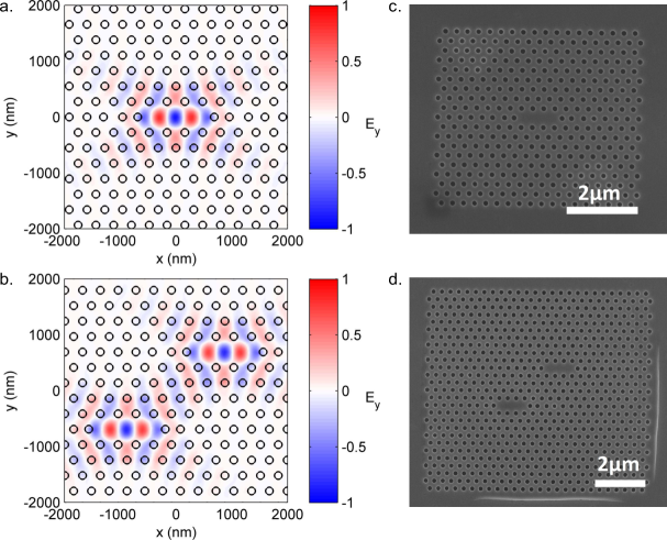
The photonic crystal cavities used in this experiment were L3 cavities in a triangular photonic crystal lattice Akahane et al. (2003), with lattice constant and design hole radius . The fundamental mode for the L3 cavity calculated using finite-difference time-domain (FDTD) simulations is plotted in figure 1a, and has a simulated quality factor of . We tested the proposed tuning mechanism on both individual cavities and pairs of proximity-coupled cavities. The coupled L3 defects were placed lattice periods apart, with a spectral splitting of calculated using FDTD. Scanning electron microscopy (SEM) images of these structures are shown in figure 1c and figure 1d.
The photonic crystal cavities were fabricated from GaAs wafers grown using molecular beam epitaxy, as described in previous works Ellis et al. (2011). The material stack consisted of a membrane and a sacrificial layer on top of a GaAs substrate. The GaAs membrane contained layers of high-density InAs quantum dots emitting at wavelengths near . The photonic crystal cavities were fabricated using electron-beam lithography, inductively-coupled plasma reactive-ion etching (ICP-RIE), and a final HF acid undercutting step, as described previously Englund et al. (2007).
The tuning was performed in a custom confocal microscopy setup coupled to a grating spectrometer with an InGaAs linear photodiode array. A Carl Zeiss LD-Plan-Neofluar was used as the microscope objective. A charge-coupled device (CCD) integrated into the microscopy setup was used to both image the sample, and determine where the lasers were focused. The experiments were all performed at room temperature in air, with the exception of an additional control test where the sample was placed in vacuum.
The photonic crystal cavities were tuned by simultaneously irradiating the sample with two lasers through the objective: the ultraviolet (UV) tuning laser, and an near-infrared pump laser to produce photoluminescence (PL) from the quantum dots embedded in the photonic crystal membranes.
For the tuning laser, we used a frequency-doubled pulsed Ti:Sapphire laser, producing an output wavelength of , pulse repetition frequency of , and an average power of before the microscope objective. The pulse length was approximately after passing through a single-mode fiber (SMF) to clean up the beam profile. The UV laser was focused either directly on or immediately adjacent to the cavity to be tuned. The spot size of the tuning laser was roughly as estimated from SEMs of tuned devices.
An , SMF-coupled continuous-wave multimode diode laser was used as the PL excitation laser. The PL laser was somewhat defocused in order to tightly focus the UV tuning laser, so it was necessary to use a relatively high power to produce a bright PL signal. Due to the Purcell effect, the spontaneous emission rate from a photonic crystal cavity is strongly enhanced at its resonant frequencies Purcell (1946). The photoluminescence spectrum was thus used to continuously monitor the cavity resonance during the tuning process. In principle, cross-polarized reflectivity measurements could also be used to monitor the cavity resonance when tuning non-photoluminescent devices Englund et al. (2007).
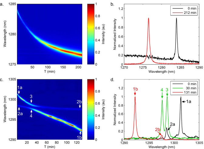
In figure 2a, we present the tuning profile of a single L3 cavity. The tuning rate decreases as a function of time, suggesting a self-limiting mechanism. The tuning rate can be increased by increasing the UV laser power, but using excessively high power risks damaging the membrane due to thermal effects. The initial and final spectra are plotted in figure 2b. The cavity quality factor is somewhat degraded by the tuning process, being reduced from to .
Next, in figures 2c and 2d we present the tuning of a single cavity in a proximity-coupled pair of L3 cavities. The behaviour of such a system can be accurately described using coupled-mode theory Haus and Huang (1991). Due to the coupling between the cavities, such a system will present two resonant peaks with frequencies given by
| (1) |
where are the individual cavity frequencies, and is the coupling between the cavities. We have assumed the cavities are in the strong coupling limit , where the is the quality factor of cavity .
The UV laser was focused on one edge of a cavity, as can be seen in an SEM of the tuned structure in figure 3a. As the UV laser was applied, the resonant peak at remained nearly stationary while the other resonant peak blueshifted from to . As the two peaks pass each other, a clear anti-crossing - which arises from equation (1) - can be observed.
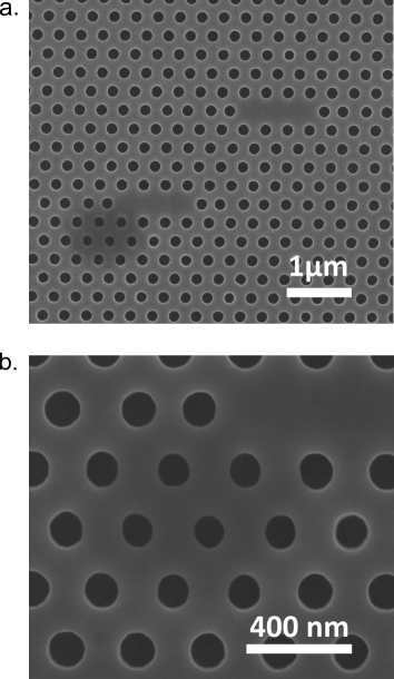
The tuning mechanism is likely photo-induced oxidation of GaAs by the UV laser, resulting in reduction of the local index of refraction and blueshifting the cavities. Previous research has shown that photo-oxidation of GaAs surfaces can be induced by UV irradiation under similar parameters to our experiment Yu et al. (1986, 1987); Lu et al. (1990). SEMs of tuned cavities are shown in figure 3. No damage to the photonic crystal is visible other than a slight discoloration and reduction in hole size in the vicinity of the irradiated spot, probably due to the growth of oxide on the surface. We also conducted identical experiments in a vacuum chamber pumped down to , and there was no observable tuning or change in appearance.
Due to the low power of our UV tuning laser, the tuning mechanism is very unlikely to be thermal oxidation. The steady state temperature increase should be very small. Based on Sentaurus simulations of similar structures, we expect to see a temperature rise of for a heat dissipation of Petykiewicz et al. (2012). We also see no permanent tuning effects from our higher power PL laser.
The instantaneous temperature rise from each UV laser pulse is expected to be much higher, but still relatively low. Assuming a plane wave propagating into an infinite slab of GaAs, and ignoring reflections, the local temperature rise from a single pulse is given by
| (2) |
where is the incident fluence , is the extinction coefficient of GaAs at Palik (1997), and are the heat capacity and density of GaAs Sze (1994), and is the distance from the incident surface. If we assume the incident light is a gaussian beam with a diameter of , the estimated temperature rise at the surface is , far too low for thermally-induced oxidation. Since we assumed there are no reflections, and used a conservative estimate of laser spot size based on our SEMs, this should be an overestimate of the actual temperature rise.
In conclusion, we have demonstrated a technique for tuning GaAs nanophotonic resonators which requires only a low-power UV laser at room temperature in ambient atmosphere. In particular, this technique can be used to independently tune individual cavities in proximity-coupled cavity configurations, allowing the fabrication of a wide range of coupled-cavity devices with applications ranging from quantum simulations and information processing to low-power nanophotonic lasers.
Acknowledgements.
The authors acknowledge support provided by the Air Force Office of Scientific Research (AFOSR) MURI Center for Multi-Functional Light-Matter Interfaces based on Atoms and Solids (FA9550-09-1-0704), and the AFOSR MURI for Complex and Robust On-chip Nanophotonics (FA9550-12-1-0025). AYP acknowledges support from the Stanford Graduate Fellowship. KGL acknowledges support from the Swiss National Science Foundation.References
- Akahane et al. (2003) Y. Akahane, T. Asano, B.-S. Song, and S. Noda, Nature 425, 944 (2003).
- Vučković et al. (2001) J. Vučković, M. Lončar, H. Mabuchi, and A. Scherer, Phys. Rev. E: Stat., Nonlinear, Soft Matter Phys. 65, 016608 (2001).
- Yoshie et al. (2004) T. Yoshie, A. Scherer, J. Hendrickson, G. Khitrova, H. M. Gibbs, G. Rupper, C. Ell, O. B. Shchekin, and D. G. Deppe, Nature 432, 200 (2004).
- Englund et al. (2007) D. Englund, A. Faraon, I. Fushman, N. Stoltz, P. Petroff, and J. Vučković, Nature 450, 857 (2007).
- Ellis et al. (2011) B. Ellis, M. A. Mayer, G. Shambat, T. Sarmiento, J. Harris, E. E. Haller, and J. Vučković, Nature Photonics 5, 297 (2011).
- Shambat et al. (2011) G. Shambat, B. Ellis, A. Majumdar, J. Petykiewicz, M. A. Mayer, T. Sarmiento, J. Harris, E. E. Haller, and J. Vučković, Nature Communications 2, 539 (2011).
- Rivoire et al. (2009) K. Rivoire, Z. Lin, F. Hatami, W. T. Masselink, and J. Vučković, Optics Express 17, 22609 (2009).
- Liew and Savona (2010) T. C. H. Liew and V. Savona, Phys. Rev. Lett. 104, 183601 (2010).
- Bamba et al. (2011) M. Bamba, A. Imamoǧlu, I. Carusotto, and C. Ciuti, Phys. Rev. A: At., Mol., Opt. Phys. 83, 021802 (2011).
- Majumdar et al. (2012) A. Majumdar, M. Bajcsy, A. Rundquist, and J. Vučković, Phys. Rev. Lett. 108, 183601 (2012).
- Greentree et al. (2006) A. D. Greentree, C. Tahan, J. H. Cole, and L. C. L. Hollenberg, Nature Physics 2, 856 (2006).
- Kerckhoff et al. (2010) J. Kerckhoff, H. I. Nurdin, D. S. Pavlichin, and H. Mabuchi, Physical Review Letters 105, 040502 (2010).
- Yariv et al. (1999) A. Yariv, Y. Xu, R. K. Lee, and A. Scherer, Opt. Lett. 24, 711 (1999).
- Altug and Vučković (2005) H. Altug and J. Vučković, Opt. Express 13, 8819 (2005).
- Hennessy et al. (2005) K. Hennessy, A. Badolato, A. Tamboli, P. M. Petroff, E. Hua, M. Atatüre, J. Dreiser, and A. Imamoǧlu, Appl. Phys. Lett. 87, 021108 (2005).
- Speijcken et al. (2012) N. W. L. Speijcken, M. A. D ndar, A. C. Bedoya, C. Monat, C. Grillet, P. Domachuk, R. Nötzel, B. J. Eggleton, and R. W. van der Heijden, Appl. Phys. Lett. 100, 261107 (2012).
- Vignolini et al. (2010) S. Vignolini, F. Riboli, D. S. Wiersma, L. Balet, L. H. Li, M. Francardi, A. Gerardino, A. Fiore, M. Gurioli, and F. Intonti, Appl. Phys. Lett. 96, 141114 (2010).
- Cai et al. (2013) T. Cai, R. Bose, G. S. Solomon, and E. Waks, Appl. Phys. Lett. 102, 141118 (2013).
- Faraon et al. (2008) A. Faraon, D. Englund, D. Bulla, B. Luther-Davies, Benjamin, J. Eggleton, N. Stoltz, P. Petroff, and J. Vučković, Appl. Phys. Lett. 92, 043123 (2008).
- Lee et al. (2009) H. S. Lee, S. Kiravittaya, S. Kumar, J. D. Plumhof, L. Balet, L. H. Li, M. Francardi, A. Gerardino, A. Fiore, A. Rastelli, and O. G. Schmidt, Appl. Phys. Lett. 95, 191109 (2009).
- Hennessy et al. (2006) K. Hennessy, C. Högerle, E. Hu, A. Badolato, and A. Imamolu, Appl. Phys. Lett. 89, 041118 (2006).
- Intonti et al. (2012) F. Intonti, N. Caselli, S. Vignolini, F. Riboli, S. Kumar, A. Rastelli, O. G. Schmidt, M. Francardi, A. Gerardino, L. Balet, L. H. Li, A. Fiore, and M. Gurioli, Appl. Phys. Lett. 100, 033116 (2012).
- Luxmoore et al. (2012) I. J. Luxmoore, E. D. Ahmadi, B. J. Luxmoore, N. A. Wasley, A. I. Tartakovskii, M. Hugues, M. S. Skolnick, and A. M. Fox, Appl. Phys. Lett. 100, 121116 (2012).
- Gong et al. (2010) Y. Gong, B. Ellis, G. Shambat, T. Sarmiento, J. S. Harris, and J. Vučković, Optics Express 18, 8781 (2010).
- Purcell (1946) E. M. Purcell, Phys. Rev. 69, 681 (1946).
- Haus and Huang (1991) H. A. Haus and W. Huang, Proceedings of the IEEE 79, 1505 (1991).
- Yu et al. (1986) C. Yu, D. Podlesnik, M. Schmidt, H. Gilgen, and R. O. Jr., Chem. Phys. Lett. 130, 301 (1986).
- Yu et al. (1987) C. F. Yu, M. T. Schmidt, D. V. Podlesnik, , and R. M. Osgood, J. Vac. Sci. Technol. B 5, 1087 (1987).
- Lu et al. (1990) Z. Lu, M. T. Schmidt, D. V. Podlesnik, C. F. Yu, and R. M. Osgood, J. Chem. Phys. 93, 7951 (1990).
- Petykiewicz et al. (2012) J. Petykiewicz, G. Shambat, B. Ellis, and J. Vučković, Applied Physics Letters 101, 011104 (2012).
- Palik (1997) E. D. Palik, Handbook of Optical Constants of Solids (Elsevier Inc., 1997).
- Sze (1994) S. M. Sze, Semiconductor Sensors (John Wiley & Sons, 1994) p. 535.