Architectural considerations in the design of a superconducting quantum annealing processor
Abstract
We have developed a quantum annealing processor, based on an array of tunably coupled rf-SQUID flux qubits, fabricated in a superconducting integrated circuit process[1]. Implementing this type of processor at a scale of 512 qubits and 1472 programmable inter-qubit couplers and operating at has required attention to a number of considerations that one may ignore at the smaller scale of a few dozen or so devices. Here we discuss some of these considerations, and the delicate balance necessary for the construction of a practical processor that respects the demanding physical requirements imposed by a quantum algorithm. In particular we will review some of the design trade-offs at play in the floor-planning of the physical layout, driven by the desire to have an algorithmically useful set of inter-qubit couplers, and the simultaneous need to embed programmable control circuitry into the processor fabric. In this context we have developed a new ultra-low power embedded superconducting digital-to-analog flux converters (DACs) used to program the processor with zero static power dissipation, optimized to achieve maximum flux storage density per unit area. The 512 single-stage, 3520 two-stage, and 512 three-stage flux-DACs are controlled with an XYZ addressing scheme requiring 56 wires. Our estimate of on-chip dissipated energy for worst-case reprogramming of the whole processor is . Several chips based on this architecture have been fabricated and operated successfully at our facility, as well as two outside facilities (see for example [2]).
Index Terms:
Superconducting integrated circuits, Quantum computing, Computational physicsI Introduction
Proposed implementations of quantum computers capable of solving problems at a useful scale generally involve at least many thousands of qubits. Whether the algorithm envisioned is based on the quantum circuit model, or on an adiabatic method, there are a number of physical requirements that constrain the design of a large-scale manufactured quantum device. The device architecture must facilitate precise individual qubit control, computationally interesting interaction between qubits, and high fidelity readout of qubit state. Of particular importance are the practical constraints that arise in acheiving these design goals while maintaining the carefully engineered environment required to implement a quantum algorithm.
One of the advantages of an approach based on superconducting qubits is that a largely compatible classical electronics technology is known and available in the guise of single-flux-quanta based circuit architectures. The authors have previously presented the architecture, design, and operation of an SFQ based system for controlling[3] and reading out[4] a quantum annealing processor based on flux qubits[1, 5] at the core of D-Wave One™ system. The authors, as well as a number of other researchers, have gained some experience using this first generation processor [6, 7, 8, 9]. This experience has informed and guided the design of a second generation quantum annealing processor, the D-Wave Two™ system. In this paper we provide an overview of this processor’s architecture and discuss some of the considerations and trade-offs involved in its design.
At the root of the design problem is the operation of a quantum annealing processor based on superconducting flux qubits. Many of the processor building blocks are described by Harris, et al.[1, 10]. A number of the control terminals (biases) required by the qubits and inter-qubit couplers are discussed by Johnson et al.[3], and these are largely unchanged. The implementation of the control circuitry, the cross section of the fabrication process, and the number of devices used, are among the main differences between the two generations of D-Wave processors.
The D-Wave One used current biased SFQ [11, 12] demultiplexer circuitry to address all programmable devices on chip, requiring an asymptotically optimal number of control lines. This circuitry was designed with consideration for the need to minimize static power dissipated on chip during programming, and to this end used very low bias supply voltages, and very low value shunt resistors. The predicted peak temperature of the junction shunts during programming, about , was sufficiently low to ensure negligible thermally induced bit errors in DAC programming.
We found, however, that it took of order for this heat to dissipate sufficiently for the processor to return to , a temperature low enough to run the quantum annealing algorithm and obtain solutions to posed problems with appreciable probability. As typical computation time is , this was clearly an unacceptable amount of time to wait to run the algorithm after programming.
D-Wave Two control circuitry was designed to eliminate static power dissipation completely and to simplify the design greatly with XYZ addressing scheme requiring lines. Though not logarithmic, this scaling is sufficiently weak to allow processors significantly larger than the one under discussion to be operated in our existing apparatus.
Improvement in performance of the annealing algorithm was also a central design goal of the D-Wave Two. In a fixed temperature environment, performance can be improved by increasing the qubit energy scale. This can be done by decreasing qubit inductance and capacitance. Given constraints on dielectric permittivity and wiring geometry, this is most practically accomplished in our design by reducing the physical length of the qubit wiring. Reduction of length by a factor of two compared with D-Wave One was achieved by adding two metal layers to the fabrication process, for a total of 6 superconducting metal layers. This allowed for an increase of overall processor density by a factor of four.
In the first section of this paper we will step back and discuss the requirements of the whole chip and give our rationale behind the chosen hardware graph topology (common between D-Wave One and Two) from the top-down perspective. We will then be in a position to present the chosen implementation of D-Wave Two control circuitry in bottom-up fashion. Read-out infrastructure will be described in a subsequent publication.
II Circuit Topology
D-Wave quantum annealing processors have evolved through a series of generations subject to the competing pressures exerted by computational complexity and practical implementation. They are designed to solve this problem: given hardware graph , minimize the following quadratic form over discrete variables :
with problem parameters for our current hardware.
Our current hardware graph topology, which we named Chimera, was designed to satisfy a number of common-sense requirements related to its intended use for solving optimization problems, subject to a number of physical implementation constraints.
II-A Requirements
-
1.
Non-planarity: We desire to tackle NP-complete problems, so non-planarity of the underlying graph is an important condition to making the corresponding Ising-spin problem NP-complete [13, 14]. A related motivation is that non-planarity is required to establish chains of qubits that cross each other.
-
2.
The ability to embed complete graphs: To solve Ising spin glass problems with different topologies using a single processor, it must be possible to map, or embed the problem graph into the available hardware graph. This process typically involves using chains, trees, or other connected sub-components of the hardware graph (comprising physical qubits, strongly ferromagnetically coupled to each other) to represent a single node in the problem graph (logical qubit). In the language of graph theory, we want the hardware graph to have largest possible variety of problem graphs as its minors [15]. While embedding arbitrary graphs is computationally hard, one can nonetheless determine how large of a degree complete graph can be embedded in a given size hardware graph, thus guaranteeing that all graphs up to nodes are embeddable using a straightforward prescription.
-
3.
The ability to incorporate on-chip control circuitry: While a single qubit, or a handful of them, can be precisely controlled with dedicated analog lines driven by room-temperature electronics, integrating more than a few dozen qubits on a single chip requires some on-chip control circuitry. For example, there are currently six control “knobs” for every qubit, required to make the qubits robust to fabrication variability [16], and one “knob” per coupler. Where possible, we have designed our QA processors to use static flux biases applied to target superconducting loops in order to realize most of these knobs. The desired values of flux biases are programmed into individual control devices using a relatively small number of essentially digital control lines that carry signals generated at room temperature. These the control devices combine the functions of persistent memory and digital-to-analog conversion. We call these devices flux DACs, or -DACs. From an architectural viewpoint, each -DAC is a relatively macroscopic object with a typical size of . Having several of them attached to a single qubit sets a lower bound on qubit size and influences possible qubit shapes and hardware graph topologies.
II-B Constraints
-
1.
Limited qubit fan-out: From an applications standpoint, the best option would be for each qubit to be connected to all others. However, directly implementing a complete graph in hardware for an arbitrarily large is impractical. Each qubit in our current design can be connected to only a relatively small number of other qubits before non-ideal features arise in the qubit response and the coupling energy scale (compared to , for example), becomes too small.
-
2.
Minimizing uncoupled qubit/coupler lengths: To optimize qubit energy scales and coupling strengths, neither qubits nor couplers can be designed to span an arbitrary length (e.g., full size of a large processor matrix). Ideally, all qubit length should be magnetically coupled to connected couplers, and all coupler length to connected qubits.
-
3.
Minimization of noise pick-up areas and cross-talks: Flux qubits and couplers are rf SQUIDs, which can be quite sensitive to magnetic fields. Extreme care needs to be taken to minimize their pick-up of undesired disturbances, such as coupling to external flux noise sources or the unintended coupling (cross-talk) from a control line to a device it is not intended to control.
-
4.
2D chip integration: While it would be nice to be able to grow a processor lattice in all three dimensions, in reality these lattices have to be implemented on the surface of 2D chips. Even if we imagine adding more metal layers to our fabrication process or 3D integration of several chips stacked on top of each other and passing quantum state between them (through, e.g., superconducting backside vias), growing the processor graph along the physical third dimension will always be harder than along the 2D chip plane.111Of course, one can attempt embedding logically higher-dimensional structures into planar chips, but this approach soon runs afoul of the second constraint above.
-
5.
Regularity and the notion of a “unit tile”: While it is in principle possible to arrange qubits in highly irregular structures, in practice, especially while designing chips not tailored to any specific problem graph structures which might arise in a concrete application, we find it convenient (to simplify the design and operation) to introduce the notion of a unit tile, which is a smaller structure that can be replicated in both dimensions of the chip plane.
II-C Chimera topology
One of the features of a flux qubit is that (unlike, e.g., qubits based on quantum dots or individual trapped ions) they are essentially macroscopic inductive loops interrupted by Josephson junction(s) and that these qubit body loops can be stretched and routed as needed. The same is true for qubit-to-qubit couplers [17, 18, 19], except that parametrically they tend to be lower inductance devices, and thus, shorter.
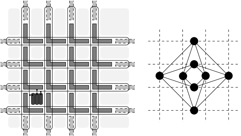
With this in mind we examined different arrangements of qubit loops, and eventually settled on the Chimera unit tile topology (used in both D-Wave One and D-Wave Two processors), schematically depicted in Fig. 1. Each unit tile consists of 8 qubits – 4 horizontal and 4 vertical – with couplers between each horizontal/vertical pair. The unit tile is a complete bipartite graph . Unit tiles can be arranged into larger grid-like structures that fill a plane, and each horizontal qubit can be coupled to the corresponding qubits in the neighboring tiles to the left and right, while each vertical qubit can be coupled to those in the neighboring tiles above and below.
How well does the Chimera topology satisfy the requirements and constraints given above? Consider the following:
-
•
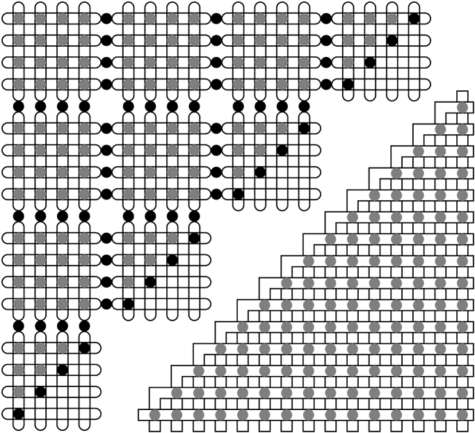
The Chimera graph is non-planar. Assuming the ability to establish chains of qubits along rows and columns of the processor matrix, there is a straightforward approach to embed complete graphs up to nodes in a grid of unit cells (denoted as ). This is illustrated in Fig. 2 for the case of . This approach can be validated based on the following observations:
-
1.
Taking a single tile and ferromagnetically coupling pairs of horizontal and vertical qubits along its diagonal (contracting edges, which connect them in graph-theoretical language) produces a complete graph .
-
2.
Taking a array of complete bipartite graphs and ferromagnetically coupling pairs of qubits in the same row/column produces a complete bipartite graph .
-
3.
Taking two complete graphs and connecting them to two sides of a complete bipartite graph produces a complete graph - every node in can be coupled to every other node either because they either belong to the same and were coupled anyway or because they belong to different s, in which case there is connection between them through the complete bipartite part.
-
1.
-
•
The Chimera topology was designed to be interleaved with the required control circuitry (which is schematically represented by lighter shaded areas in Figure 1). In the implementation under discussion, each square “plaquette” formed at the intersection of two qubits contains three -DACs. Generally, the left (right) -DAC provides certain type of control to the vertical (horizontal) qubit, while the middle one controls the corresponding coupler, as schematically shown in the bottom-left corner of this diagram.
-
•
Almost all of the qubit length is coupled to couplers, and almost all of the coupler length is coupled to qubits, thus maximizing coupled signal strength. Also, implementing the qubit and coupler loops as long and narrow differential microstrip lines (in practice, over a superconducting ground-plane) minimizes noise and parasitic cross-talk pick-up.
-
•
Chimera unit tiles can be arranged into arbitrarily large 2D structures (limited only by fabrication yields, die size and available number of IO lines/die pads required to program all -DACs). For example, the D-Wave One processor contained 128 qubits in a grid (a grid of 8-qubit tiles) and the D-Wave Two processor contains 512 qubits in a grid (an grid of 8-qubit tiles).
While this approach can be generalized to an arbitrary unit tile with qubits, our current implementation of was chosen because (as will be seen later) all of its required -DACs can be fit in a array of fixed-size plaquettes without too much wasted space, simplifying (manual) layout and managing overall design complexity. Another advantageous feature of the size is that the number of -DACs used for problem specification (one per qubit and one per coupler, thus giving a total of 32 per tile) is approximately balanced with the number of -DACs used to make qubits robust against fabrication variations (4 per qubit in the D-Wave One generation, 5 in D-Wave Two, giving a total of 32 or 40 per tile, respectively). For smaller unit tile size majority of the -DACs would be of the second variety.
III Design and operation of a -DAC.
The precision desired for setting problem parameters sets the requirements for the range and precision of individual -DACs. Generally, our current implementation requires about 8 bits of dynamic range for individual -DACs, with full ranges varying from several thousandths of a magnetic flux quantum () to half a coupled into qubit or coupler control loops, depending on the -DAC type.
To achieve this dynamic range while minimizing both total area occupied by control circuitry (thus minimizing qubit length and increasing qubit energy scales) and total number of wires needed for programming, in our current design we chose to implement most of our -DACs as two-stage devices, of the kind schematically shown in Figure 3.
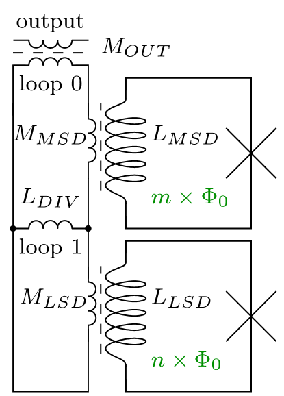
Each of the DAC digits (referred to as “most significant” and “least significant” here, or “MSD” and “LSD”) is implemented as a SQUID loop into which we can write and store some number of flux quanta , e.g., . Individual quanta can be added to or subtracted from the storage loop via an SFQ pulse source, depicted here as a Josephson junction; its structure and operation will be described in section III-B. Both digit storage loops are magnetically coupled into an output device via an inductive ladder.
A single flux quantum added to the MSD coil induces flux into the top ladder loop, and into the output device ( denotes total inductance of the MSD loop). The output flux increases proportinally with the number of flux quanta added, up to a maximum determined by the device parameters and addressing scheme. There is in general a nonlinear component associated with the junction inductances, but as long as these inductances are small compared to main loop inductances (true for our devices), this correction is negligible. In our example, if MSD loop can store up to 8 flux quanta of either polarity, it can provide 16 distinct values of output flux, or implement a 4-bit DAC.
To increase precision, a second stage is added. Here, the effect of a single flux quantum in the LSD loop is further subdivided by a factor of . If this loop can also provide 16 distinct values of stored flux and the division ratio is 16, one MSD step will be further subdivided into 16 steps of LSD, and the two-stage device is an 8-bit DAC.
In practice, of course, we want to guarantee both the total output range and the coverage of an MSD step by the LSD in the presence of fabrication variations, so we need to add some margin to the number of quanta that we can store in both loops.
-DACs with different numbers of digits and weights of each digit can be designed using the same principles, but we have found that this two-stage design is sufficient for almost all of our DACs222Two special cases were introduced in D-Wave Two processors: a DAC which biases the qubit CCJJ major loop, for which currently 5 bits of dynamic range is sufficient and it was implemented as a single coil of the same type directly coupled into a target device, and second a very coarse stage for a qubit flux bias DAC, useful to deal with larger local qubit flux offsets..
III-A -DAC: Inductive storage and ladder
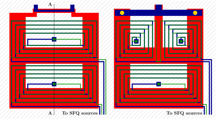
Having covered the basic idea behind our -DACs, we can present a more realistic layout of their implementation on the top of Figure 4. Large storage inductors () are implemented as stacked spirals (blue and green in the figure), shown here wound in two metal layers, though our real layouts use four layer spirals, with line width and spacing design rules.
The inductive ladder is implemented as two galvanically connected washers in the bottom metal layer (red), magnetically coupled to their two coils. The horizontal bar between them implements the shared inductance of Figure 3.
To minimize unintended coupling between DAC coils and other elements of the circuit, the whole structure is covered by a shielding sky-plane in the top metal layer (dotted diagonal lines).

| Weight of one SFQ in LSD loop, | = | ||
| Weight of one SFQ in MSD loop, | = | ||
| LSD capacity, | = | ||
| MSD capacity, | = | ||
| Division ratio, should be | |||
| Total range, | = | ||
| Effective dynamic range, bits |
Simple magnetic coupling between the inductive ladder and target device using the microstrip transformer shown in the top-left panel of Figure 4 is sufficient to implement a full range of several tens of into the target device. However, the majority of our DACs (ones that control the compound Josephson junctions of couplers, inductance tuners and persistent current compensators) require a range comparable to half a , since they need to be able to bias their target’s corresponding CJJ all the way between its maximum and fully suppressed. To implement such higher-range control we merge the CJJ loop of the target device with the MSD stage of the inductive ladder, as shown in the top-right panel of Figure 4 (Josephson junctions are shown as yellow circles).
An additional complication of this particular structure is that the DAC should be coupled with equal strength into both halves of the target CJJ loop in order to avoid coupling into target device body. To achieve this, the MSD coil is split into two symmetric halves, as shown in the top-right panel of Figure 4.
The simplistic lumped-element model of Figure 3 is not entirely adequate as a complete description of our -DAC devices, especially considering the cross-section of an actual device implemented in all six available metal layers (drawn to scale) at the bottom of Figure 4. The LSD loop couples flux directly into the MSD one and it can reach the output not only via the inductive ladder, but also via this magnetic connection to the (strongely coupled to the output) MSD. In addition, the MSD flux can reach the output directly, not mediated by the washer (and with the sign opposite to the washer-mediated coupling).
We treat a complete -DAC structure as a three-port device (LSD, MSD and OUT) and, using the 3D inductance extraction program FastHenry with superconductor support [20], extract its complete inductance matrix:
For subsequent analysis we treat the SFQ pulse sources as simple current sources that can produce (up to) (approximately half of their junction critical current , as discussed below) into a large inductive load, and calculate all relevant parameters of our -DACs as shown in Table I. After we build a -DAC layout model, we iterate over its geometrical parameters to ensure that it fits into the available space, has the required number of bits and range, and that its MSD/LSD division ratio is such that the LSD comfortably spans a single MSD step.
III-B -DAC: SFQ pulse sources
Our implementation of an SFQ source is based on perhaps the earliest incarnations of single-flux-quanta circuits [21]: a current biased dc-SQUID made with two shunted junctions.
A schematic of two dc-SQUIID SFQ pulse sources feeding the LSD and MSD storage loops of a single -DAC is shown in Figure 5.

To operate, one first applies PWR current bias (biasing all junctions to about half of their ). ADDR is then applied, providing an initial flux bias to the dc-SQUID bodies. Ramping TRIG with a polarity that adds to ADDR in, for example, the dc-SQUID comprised of junctions J0 and J1, eventually steers enough current through J0 to exceed its critical current, causing it to “flip” by in phase, admitting a single flux quantum into the dc-SQUID loop. TRIG is then decreased, eventually causing J1 to flip. The J0/J1 dc-SQUID is thus returned to its zero flux state, but in the process the phase drop across the LSD inductor has been increased by – an SFQ pulse is added to that storage loop. Assuming the LSD inductor is large compared to the dc-SQUID inductance, this process can be repeated until the persistent current stored in the LSD loop becomes comparable to the PWR current, cancelling it, preventing junctions from further flipping. At that point, the -DAC loop has reached its maximum SFQ capacity.
If one changes the sign of PWR, using the same process one can add single flux quanta of the opposite magnetic field direction into this storage loop (or, subtract from the ones stored there).
Note that the TRIG line is twisted between the dc-SQUIDs J0/J1 and J2/J3, so when it adds to the ADDR prebias for the J0/J1 dc-SQUID, it subtracts from the J2/J3 dc-SQUID, and the J2/J3 SQUID is quiescent. But if one reverses the polarity of the TRIG pulses relative to the ADDR pre-bias, one can operate the J2/J3 dc-SQUID, adding a SFQ to the MSD -DAC coil. The relative polarity of ADDR and TRIG allows us to select the -DAC stage on which we want to operate.
The PWR, ADDR, and TRIG levels are chosen to meet the following criteria:
-
1.
With PWR held at its active level, the state of a -DAC changes by exactly one flux quanta per ADDR, TRIG pulse.
-
2.
Each -DAC undergoes SFQ transitions only when all three lines addressing that device are active. If two or fewer lines are active, the state of the -DAC does not change.
If these criteria are met, then a limited number () of control lines can address -DACs in what we call “XYZ” fashion, discussed further in Section III-E. Here we discuss the process, which we refer to as margining, by which programming levels are chosen to meet the above criteria.
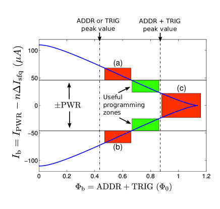
-DAC state stability is fully determined by and , where is the sum of the ADDR and TRIG flux biases and is the total current biasing the dc-SQUID SFQ pulse source. includes contributions from PWR and from the current circulating in the main -DAC loop due to its flux state. A critical line in space, similar to that of a current biased dc-SQUID, bounds the region in which a flux state is stable. When this line is crossed due to manipulation of PWR, ADDR, and TRIG, a transition will take place.
In Figure 6, the critical line of the zero flux state of the dc-SQUID pulse source is plotted. Crossing this boundary corresponds to the first junction flip in the SFQ pulse sequence described previously. The system will cross the boundary at a point that depends on the main -DAC loop flux state. Margining of the PWR, ADDR, and TRIG levels can be understood as a geometric partitioning of this boundary into active regions, in which intended transitions will take place, and forbidden zones, in which transitions that do not meet the margining criteria would occur. PWR, ADDR and TRIG levels are chosen to maximize the size of the active regions while avoiding the forbidden zones.
III-C -DAC reset
The protocols described above allow us to add or subtract SFQ to a -DAC stage, ending up with a known number of flux quanta when we start from a known state. For realistic operation we must also be able to reliably reset all -DACs into a known state starting from an unknown state.
To reset a -DAC, is set to zero. The dc-SQUID pulse source still sees a non-zero current bias, as long as the -DAC is in a non-zero flux state. Programming the -DAC under these conditions will cause SFQ changes in the main -DAC loop that decrease this current bias. Applying ADDR+TRIG pulses with large enough amplitude to reliably drive transitions (larger than the maximum value of the critical boundary in Figure 6) will ’de-program’ the -DAC one SFQ at a time, until it reaches its lowest energy zero SFQ state for which the circulating current is zero. To reliably reach this zero SFQ state, junction critical current asymmetry must be small: the critical current difference between the two junctions in the dc-SQUID pulse source should be well under , where is the main loop inductance.
Note that the margining criteria are violated during reset. All -DACs are reset simultaneously.
III-D Minimizing -DAC footprint
As we mentioned in Section II, the -DAC area is what ultimately sets the size of our processor unit tile. This in turn determined the length of the qubits, and thus their energy scales, ultimately affecting the performance of the annealing algorithm. Minimizing this area is therefore of great importance to us.
What matters for a given -DAC to achieve its design objectives is the maximum number of single flux quanta that we can store in its MSD and LSD loops (determining maximum range and precision, provided that division ratio is chosen correctly). That, in turn, is proportional to the product of the storage loop inductance and the pulse source junction . How can we minimize an area required to implement both junctions and inductor to achieve constant (and sufficient) product? Equivalently, how can we maximize this product in given area?
One can observe that (to the first order of approximation), inductance of a spiral coil (for fixed number of available layers) is proportional to its area with some proportionality constant . The same is true for junction area, given a fixed critical current density . If we have unit area available for the whole -DAC, and inductance occupies some fraction of that, , which reaches its maximum at , meaning that half of the optimal -DAC area is occupied by storage inductance and another half by source junctions.
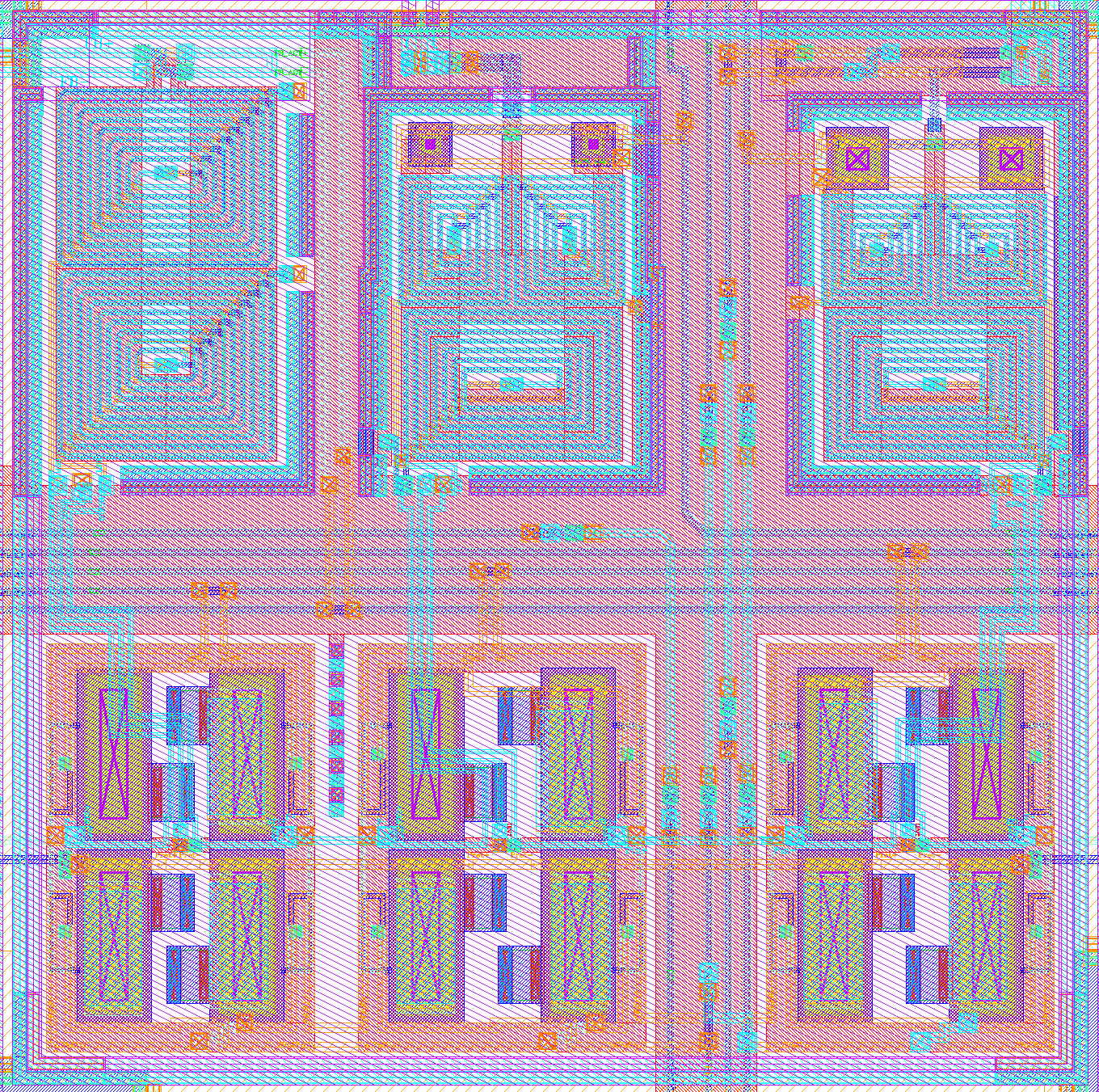
This was the rule that we used for choosing source junction vs. storage (their was fixed by requirements of the analog qubit and coupler circuitry in a process with only a single available trilayer). Figure 7 is a CAD view of three -DACs within one plaquette of our current processor.
Note that the result of this analysis is independent of critical current density. Suppose a second high- trilayer becomes available for our next generation design, say, (in addition to our current ), a factor of 36 in . Just replacing the existing junctions with smaller in size and equal critical current would save us less than a factor of 2 in -DAC area. If instead is decreased and is increased by a factor of 6 in value, the total area decreases by the same factor, with product unchanged.
III-E XYZ-addressing line count
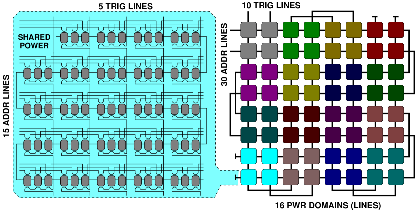
We need 72 -DACs to control all the qubits and couplers of a unit tile (6 per qubit, 16 for controlling internal couplers, and 8 for controlling external couplers), for a total of 4608 -DACs for our D-Wave Two 512-qubit processors. To select one of them using cubic XYZ-addressing, we need at least lines, or about 16 lines per dimension.
We have arranged all required -DACs for a given tile in 25 3-DAC plaquettes (one plaquette is empty), as shown in the left panel of Figure 8. One of three -DACs within a plaquette is selected using one of three ADDR lines, with all three sharing a TRIG line, resulting in 15 ADDR and 5 TRIG lines addressing all -DACs within unit tile.
The third dimension of addressing is established by separating tile arrays into PWR domains. Our D-Wave Two processors contain an array of unit tiles, split into sixteen power domains, as shown in the right panel of Figure 8. All -DACs within one power domain are connected in series and fed by one of 16 PWR lines. 30 ADDR and 10 TRIG lines are reused between power domains, for a total of lines used to address all -DACs within a processor matrix. While it is not optimal (because of the difference in the number of ADDR and TRIG lines), it is sufficiently close, and this arrangement allowed us to achieve a more regular layout without having to assign different roles to a single line within the processor fabric (e.g., make a single line work as an ADDR for one DAC and a TRIG for another).
IV Conclusions
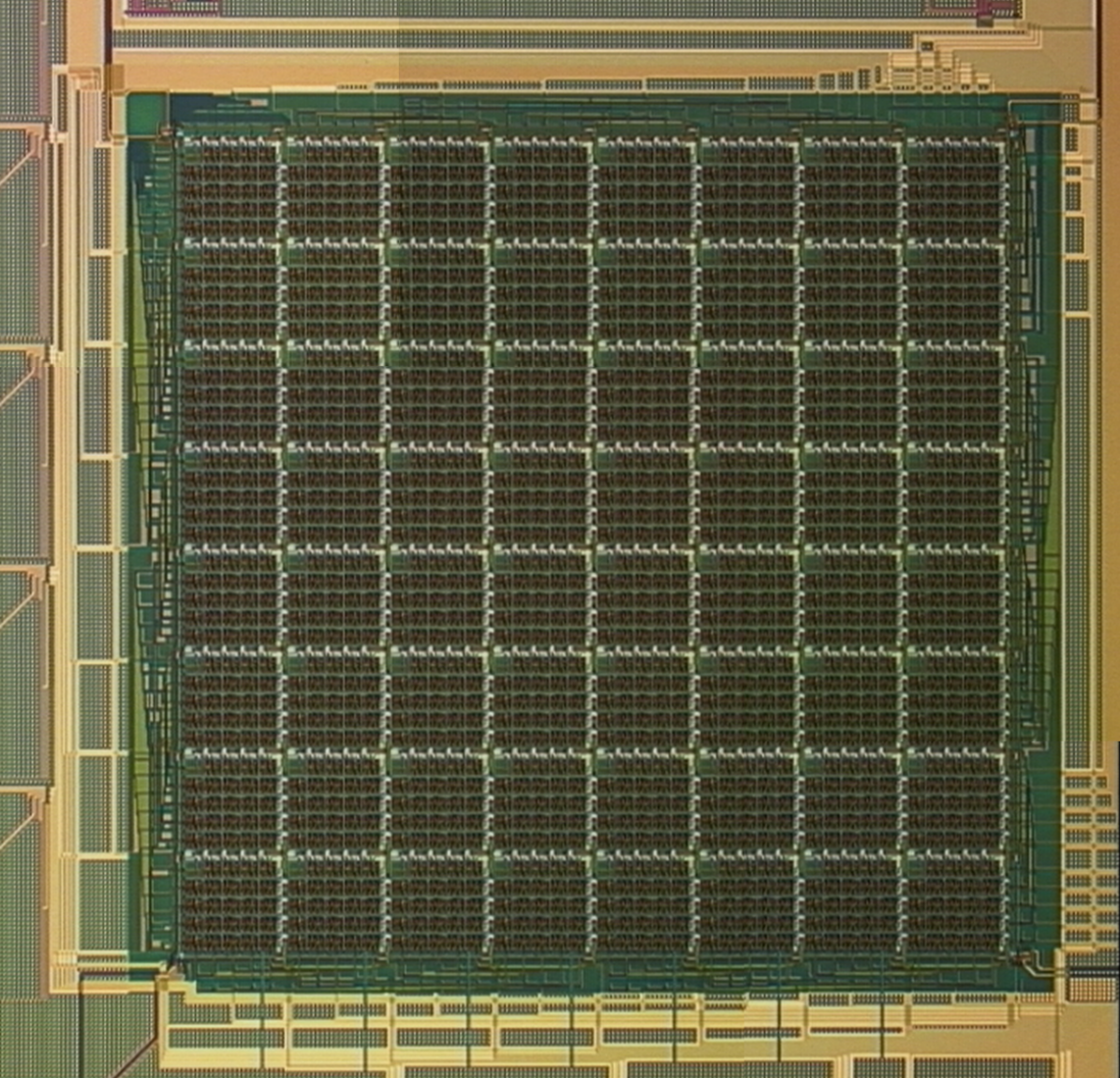
We have described how, starting with top-level requirements of a processor implementing a quantum annealing algorithm, we have designed its hardware graph and required control infrastructure, which allowed us to successfully operate processors with up to 512 rf-SQUID qubits using only 56 control lines for problem programming. Figure 9 shows a microphotograph of an active area of a D-Wave Two processor chip.
The most important feature of our new -DAC design is its zero static power dissipation – unlike traditional SFQ circuitry, which incorporates on-chip resistive current sources tapping a common voltage rail, this design biases all devices serially with a fixed current whose magnitude is set by a room-temperature resistor333This approach can also be viewed as implementing SFQ “current recycling” taken to its ultimate limit.. The only energy dissipated on-chip is on the order of per flux quantum moved into (or out of) the storage inductor. For a pair of -DAC junctions this corresponds to . Complete reprogramming of all 9216 -DAC stages moving from -16 to +16 SFQ in their storage loops would dissipate on chip only about .
While the D-Wave One required a post-programming delay of about , D-Wave Two can thermalise to within , a factor of 100 improvement achieved within one processor generation just in this post-programming thermalization time.
References
- [1] R. Harris, M. W. Johnson, T. Lanting, A. J. Berkley, J. Johansson, P. Bunyk, E. Tolkacheva, E. Ladizinsky, N. Ladizinsky, T. Oh, F. Cioata, I. Perminov, P. Spear, C. Enderud, C. Rich, S. Uchaikin, M. C. Thom, E. M. Chapple, J. Wang, B. Wilson, M. H. S. Amin, N. Dickson, K. Karimi, B. Macready, C. J. S. Truncik, and G. Rose, “Experimental investigation of an eight-qubit unit cell in a superconducting optimization processor,” Phys. Rev. B, vol. 82, p. 024511, Jul 2010. [Online]. Available: http://link.aps.org/doi/10.1103/PhysRevB.82.024511
- [2] N. Jones, “Google and NASA snap up quantum computer,” Nature News, May 16 2013.
- [3] M. W. Johnson, P. Bunyk, F. Maibaum, E. Tolkacheva, A. J. Berkley, E. M. Chapple, R. Harris, J. Johansson, T. Lanting, I. Perminov, E. Ladizinsky, T. Oh, and G. Rose, “A scalable control system for a superconducting adiabatic quantum optimization processor,” Superconductor Science and Technology, vol. 23, no. 6, p. 065004, 2010. [Online]. Available: http://stacks.iop.org/0953-2048/23/i=6/a=065004
- [4] A. J. Berkley, M. W. Johnson, P. Bunyk, R. Harris, J. Johansson, T. Lanting, E. Ladizinsky, E. Tolkacheva, M. H. S. Amin, and G. Rose, “A scalable readout system for a superconducting adiabatic quantum optimization system,” Superconductor Science and Technology, vol. 23, no. 10, p. 105014, 2010. [Online]. Available: http://stacks.iop.org/0953-2048/23/i=10/a=105014
- [5] M. W. Johnson, M. H. S. Amin, S. Gildert, T. Lanting, F. Hamze, N. Dickson, R. Harris, A. J. Berkley, J. Johansson, P. Bunyk, E. M. Chapple, C. Enderud, J. P. Hilton, K. Karimi, E. Ladizinsky, N. Ladizinsky, T. Oh, I. Perminov, C. Rich, M. C. Thom, E. Tolkacheva, C. J. S. Truncik, S. Uchaikin, J. Wang, B. Wilson, and G. Rose, “Quantum annealing with manufactured spins,” Nature, vol. 473, pp. 194–198, May 2011.
- [6] S. Boixo, T. F. Rønnow, S. V. Isakov, Z. Wang, D. Wecker, D. A. Lidar, J. M. Martinis, and M. Troyer, “Quantum annealing with more than one hundred qubits,” arXiv:1304.4595, 2013. [Online]. Available: http://arxiv.org/abs/1304.4595
- [7] K. L. Pudenz, T. Albash, and D. A. Lidar, “Error corrected quantum annealing with hundreds of qubits,” arXiv:1307.8190v1, 2013. [Online]. Available: http://arxiv.org/abs/1307.8190v1
- [8] Z. Bian, F. Chudak, W. G. Macready, L. Clark, and F. Gaitan, “Experimental determination of ramsey numbers,” Phys. Rev. Lett., vol. 111, p. 130505, Sep 2013. [Online]. Available: http://link.aps.org/doi/10.1103/PhysRevLett.111.130505
- [9] H. Neven, V. S. Denchev, M. Drew-Brook, J. Zhang, W. G. Macready, and G. Rose, “Nips 2009 demonstration: Binary classification using hardware implementation of quantum annealing,” NIPS 2009: Demonstration (Quantum), pp. 1–17, 2009.
- [10] R. Harris, J. Johansson, A. J. Berkley, M. W. Johnson, T. Lanting, S. Han, P. Bunyk, E. Ladizinsky, T. Oh, I. Perminov, E. Tolkacheva, S. Uchaikin, E. M. Chapple, C. Enderud, C. Rich, M. Thom, J. Wang, B. Wilson, and G. Rose, “Experimental demonstration of a robust and scalable flux qubit,” Phys. Rev. B, vol. 81, p. 134510, Apr 2010. [Online]. Available: http://link.aps.org/doi/10.1103/PhysRevB.81.134510
- [11] K. K. Likharev and V. K. Semenov, “RSFQ logic/memory family: a new Josephson junction technology for sub-teraherz clock frequency digital systems,” IEEE Trans. Appl. Supercond., vol. 1, no. 1, pp. 3–28, March 1991.
- [12] P. Bunyk, K. Likharev, and D. Zinoviev, “Rsfq technology: Physics and devices,” International journal of high speed electronics and systems, vol. 11, no. 01, pp. 257–305, 2001.
- [13] F. Barahona, “On the computational complexity of ising spin glass models,” Journal of Physics A: Mathematical and General, vol. 15, no. 10, p. 3241, 1982. [Online]. Available: http://stacks.iop.org/0305-4470/15/i=10/a=028
- [14] S. Istrail, “Statistical mechanics, three-dimensionality and np-completeness: I. universality of intracatability for the partition function of the ising model across non-planar surfaces,” in Proceedings of the thirty-second annual ACM symposium on Theory of computing. ACM, 2000, pp. 87–96.
- [15] V. Choi, “Minor-embedding in adiabatic quantum computation: I. the parameter setting problem,” Quantum Information Processing, vol. 7, no. 5, pp. 193–209, 2008. [Online]. Available: http://dx.doi.org/10.1007/s11128-008-0082-9
- [16] R. Harris, J. Johansson, A. J. Berkley, M. W. Johnson, T. Lanting, S. Han, P. Bunyk, E. Ladizinsky, T. Oh, I. Perminov, E. Tolkacheva, S. Uchaikin, E. M. Chapple, C. Enderud, C. Rich, M. Thom, J. Wang, B. Wilson, and G. Rose, “Experimental demonstration of a robust and scalable flux qubit,” Phys. Rev. B, vol. 81, no. 13, p. 134510, Apr 2010.
- [17] A. Maassen van den Brink, A. J. Berkley, and M. Yalowsky, “Mediated tunable coupling of flux qubits,” New Journal of Physics, vol. 7, no. 1, p. 230, 2005. [Online]. Available: http://stacks.iop.org/1367-2630/7/i=1/a=230
- [18] R. Harris, A. J. Berkley, M. W. Johnson, P. Bunyk, S. Govorkov, M. C. Thom, S. Uchaikin, A. B. Wilson, J. Chung, E. Holtham, J. D. Biamonte, A. Y. Smirnov, M. H. S. Amin, and A. Maassen van den Brink, “Sign- and magnitude-tunable coupler for superconducting flux qubits,” Phys. Rev. Lett., vol. 98, p. 177001, Apr 2007. [Online]. Available: http://link.aps.org/doi/10.1103/PhysRevLett.98.177001
- [19] R. Harris, T. Lanting, A. Berkley, J. Johansson, M. Johnson, P. Bunyk, E. Ladizinsky, N. Ladizinsky, T. Oh, and S. Han, “Compound josephson-junction coupler for flux qubits with minimal crosstalk,” Physical Review B, vol. 80, no. 5, p. 052506, 2009.
- [20] [Online]. Available: http://www.wrcad.com/ftp/pub/README.FASTHENRY
- [21] J. P. Hurrell, D. C. Pridmore-Brown, and A. H. Silver, “Analog-to-digital conversion with unlatched squid’s,” IEEE Transactions on Electron Devices, vol. 27, pp. 1887–1896, Oct 1980.