Optical Absorption Measurement at 1550 nm on a Highly-Reflective Si/SiO2 Coating Stack
Abstract
Future laser-interferometric gravitational wave detectors (GWDs) will potentially employ test mass mirrors from crystalline silicon and a laser wavelength of 1550 nm, which corresponds to a photon energy below the silicon bandgap. Silicon might also be an attractive high-refractive index material for the dielectric mirror coatings. Films of amorphous silicon (a-Si), however, have been found to be significantly more absorptive at 1550 nm than crystalline silicon (c-Si). Here, we investigate the optical absorption of a Si/SiO2 dielectric coating produced with the ion plating technique. The ion plating technique is distinct from the standard state-of-the-art ion beam sputtering technique since it uses a higher processing temperature of about 250∘C, higher particle energies, and generally results in higher refractive indices of the deposited films. Our coating stack was fabricated for a reflectivity of for s-polarized light at 1550 nm and for an angle of incidence of 44∘. We used the photothermal self-phase modulation technique to measure the coating absorption in s-polarization and p-polarization. We obtained and . These results correspond to an absorption coefficient which is lower than literature values for a-Si which vary from up to . It is, however, still orders of magnitude higher than expected for c-Si and thus still too high for GWD applications.
1 Introduction
Highly-reflective (HR) dielectric mirror coatings are essential for interferometric gravitational wave detectors (GWDs). Optical coatings with low optical absorption and low mechanical loss are required [1]. It is expected that mechanical loss in optical coatings will result in a significant thermal noise source in GWDs of the 2nd generation, which are currently under construction [2]. The 2nd generation of GWDs will operate at the well-established laser wavelength of 1064 nm and will use well-established dielectric optical coatings made of alternating layers of silica (SiO2) and tantala (Ta2O5). The test mass mirror HR coatings for the 1st generation LIGO GWDs [3] had a design transmission of 5 ppm [4] and an absorption requirement of . For the 2nd generation Advanced LIGO GWDs the optical absorption needs to be less than 0.5 ppm [1, 4]. While coatings with the specified absorption requirement were already produced [1], the mechanical loss realized is still above the requirement of [4], at which tantala contributes most to the coating’s mechanical loss [2]. Doping the tantala with titanium reduces the loss by nearly a factor of two, but slightly increases the coating absorption [1]. In addition, titanium doped tantala shows a loss peak at low temperatures [5], where some of the 3rd generation GWDs will operate [6]. Therefore various materials are under investigation to replace tantala within dielectric coatings [7].
Because of its high mechanical Q-factor at cryogenic temperatures [9, 8], crystalline silicon (c-Si) is considered as a test-mass material [7] for future GWDs. c-Si shows a high optical absorption at 1064 nm. Since the absorption decreases rapidly toward higher wavelengths [10], the use of c-Si test masses is planned at a wavelength of 1550 nm, which corresponds to a photon energy below the silicon band gap. Silicon might also be an interesting candidate for a coating material in view of replacing tantala. The high index of refraction of Si of at 1550 nm [11] significantly reduces the number of single layers required to achieve high reflectivities. It also reduces the geometrical thickness of the coating stack, since a single layer has a constant optical thickness of about a quarter of the wavelength. The optical as well as the mechanical loss of the Si films, however, need to be less than the values for tantala. Dielectric coating stacks usually contain amorphous material, and amorphous Si (a-Si) is known to be rather absorptive at 1550 nm [13, 12, 14]. In [12] it is reported that annealing of a-Si reduces the absorption coefficient of the material. The a-Si in [12] was produced with radio-frequency sputtering.
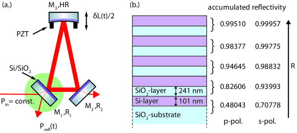
In this work we present optical absorption measurements at 1550 nm on a highly-reflective Si/SiO2 coating produced with the ion plating technique. The coating was produced with high particle energies between 30 eV and 50 eV, a high processing temperature of about , and was finally annealed at . The coating was fabricated by Tafelmaier Dünnschicht-Technik GmbH [15] and optimized for a reflectivity of at 1550 nm in s-polarization and an angle of incidence (AOI) of . The ion plating technique is distinct from today’s state-of-the-art ion beam sputtering technique since it uses a higher processing temperature, higher particle energies, and generally results in higher refractive indices of the deposited films. The optical absorption of Si-films produced with this technique is not known. Our absorption measurement was performed in a three-mirror ring-cavity setup (see Fig. 1 (a.)) in s- and p-polarization using the photothermal self-phase modulation technique [16, 17]. The actual design of the coating stack was not at our disposal. Therefore, we used a model coating stack [18] that matched our measurement results for the reflectivities in s- and p-polarization. From this model we calculated the absorption coefficient of the Si layers taking into account an effective penetration depth of the laser beam.
2 Experimental setup and results
The technique of photothermal self-phase modulation (PSM) allows coating absorption measurements, if the substrate that carries the mirror coating is used as the incoupling mirror of an optical cavity [16, 17]. For our experiment we used a three-mirror ring-cavity formed by the plane in-coupling mirror and end-mirror together with the concave highly-reflective (HR) coated mirror (see Fig. 1 (a.)). All three mirrors had substrates from Corning 7980 glass [19]. All coatings were manufactured by Tafelmaier [15] using the ion plating technique. The coatings of and were produced in the same coating run and designed for a reflectivity of at an angle of incidence (AOI) of for a wavelength of 1550 nm and s-polarization. The HR coating of had negligible transmission compared to the transmissions of and . The mirror substrate parameters and cavity geometry parameters are presented in Tab. 1.
| Material parameters | Cavity geometry parameters | ||
| (at and room temperature) | |||
| index of refraction | [20] | round-trip length | 42 cm |
| thermal refr. coeff. d/d | [20] | beam waist (radius) | 448 m |
| specific heat | [21] | mirror length | 6.35 mm |
| density | [19] | mirror radius | 12 mm |
| thermal expansion | [19] | AOI | |
| thermal conductivity | [19] | ||
The three mirrors forming the cavity were glued to an aluminum spacer. In the course of our PSM technique, the cavity length was scanned and the shapes of the cavity resonance peaks were recorded. A piezoactuator (PZT) between and the spacer was used to modulate the cavity round-trip length. To minimize a potential nonlinear motion of the PZT the cavity length was scanned only in a small range around a cavity resonance of approximately 10 % of a free spectral range. The modulation voltage was constant for all measurements. To compensate for an remaining nonlinearity of the PZT motion as well as to compensate for a potential PZT hysteresis the actual mirror motion for each modulation frequency and ramp side (expansion or contraction of the PZT) was calibrated using phase-modulation side-bands imprinted on the laser signal via an electro optical modulator (EOM) before entering the cavity. The resonance peaks for the absorption measurements were detected in reflection of with a photo diode (PD).
In this setup, the PSM technique provides the absorption of the coating of the in-coupling mirror . While the intra-cavity field builds up, the coating absorbs light. The resulting heat is transferred to the substrate of the incoupling mirror and the in-coupled beam receives a phase shift due to the change of the optical path length through resulting in a broadening and narrowing of the cavity resonance peak. At the same time absorption in the coatings of all three mirrors result in thermal expansion of the mirrors, which shortens the cavity round-trip length. The measured deformation of the cavity resonance peaks is, however, clearly dominated by the first effect.
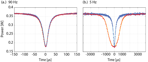
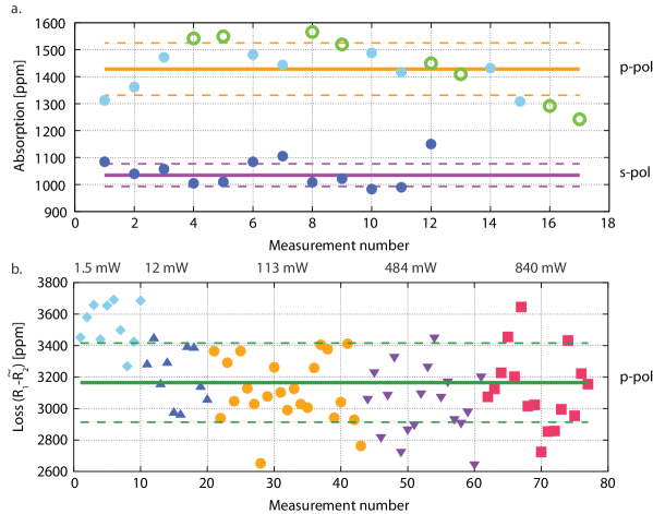
A pair of two deformed resonance peaks – one for shortening and one for lengthening the cavity – allowed us to obtain the quantities , and . is the power reflectivity of in-coupling mirror , whereas is the effective reflectivity of that includes all cavity round-trip losses apart from the transmission of , and is the absorption of the coating of . A measurement of such a pair of resonance peaks we shall call in the following a single measurement. To reduce errors due to statistical fluctuations, several single measurements were performed. For every single measurement a Nelder-Mead algorithm varied , and , and thus minimized the deviation between simulated and measured data. The single measurements were carried out with different scan velocities to exclude systematic effects. For p-polarization, in addition to the scan frequency also the input power was varied to exclude intensity-dependent effects that were found in c-Si [22, 23]. The results for our single measurements are shown in Fig. 3 (a.). The upper light-blue dots show results at an input power of 484 mW, the green circles show the results taken at an input power of 840 mW. Further, the round-trip loss was measured at input powers of 1.5 mW (), 12 mW (), 113 mW (), 484 mW () and 840 mW (). For p-polarization, the result is . The results for the reflectivities are and . Since in p-polarization no power dependence occurred, in s-polarization the input power was kept constant at 367 mW, while the scan frequency was varied between 5 Hz and 500 Hz. Figure 2 (a.) shows resonance peaks (external lengthening: red dots – measurement, orange line – simulation; external shortening: blue dots – measurement, light-blue line – simulation) detected at a scan frequency of 90 Hz, where the two peaks for an external lengthening and shortening of the cavity were identical. A frequency of about 15 Hz was the limit at which the thermal effect was sufficient for fitting . The results of the single measurements for s-pol are presented in Fig. 3 (a.) (lower, dark-blue dots). The mean value (lower, purple line) and standard deviation (lower, purple dashed lines) of the results from the single measurements is . The results for the reflectivities are and (= round-trip loss). Our measured value of is in perfect agreement with the design reflectivity.
In the following, the influence of potential errors in the simulation input parameters on our results is analyzed. Therefore, we simulated the influence of the individual parameters listed in Tab. 1 on our result beginning with the material parameters, which we took from the literature. The errors of the refractive index as well as of the thermal refractive coefficient d/d were found to be negligible [20]. An error of the thermal expansion was also negligible since d/d by far dominates the phase shift of the laser beam [17]. Changes of the specific heat and density affected the absorption result approximately linearly. A change by 10 % of the thermal conductivity affected the result by about 4 %. Potential errors in the cavity geometry parameters were also found to be negligible. The mirror length and mirror radius did not affect our absorption result for , which is valied for our setup. A measurement error of the round trip length of 420 mm was estimated to be and was thus negligible as well. and beam waist were based on and potential errors in these quantities were also negligible. We thus conclude that the standard deviation of our measurements also includes potential errors of the input parameters if we assume that the errors of the parameters are statistically independent.
3 Discussion and Conclusion
For our dielectric Si/SiO2 coating produced with ion plating, absorption values of and were measured. These values are orders of magnitude higher than the optical absorption of state-of-the-art SiO2/Ta2O5 coatings being in the ppm regime [24, 17].
To transfer our results to an absorption coefficient for the deposited silicon layers, the layout of the actual dielectric Si/SiO2 coating stack is required. Since the actual design was not at our disposal, we used a model coating stack that matched our measurement results for the reflectivities in s- and p-polarization of using [18]. was the best matching set that could be achieved. Figure 1 (b.) shows a schematic of the simulated coating stack including the thicknesses per single layer. The simulated reflectivity after each double layer is given on the right side in Fig. 1 (b.). Since the individual double layers transmit only a fraction of the laser power, the absorption coefficient needs to be based on an effective penetration depth, here given in units of double layers
where the numbers are taken from Fig. 1 for s-polarized light. As the result, effectively 1.37 double layers are transmitted twice by 100 % of the input power. Assuming the absorption in the SiO2 layers to be negligible [24, 17], this results in an absorption coefficient of for the silicon layers. The factor 1.02 is a correction of the layer thickness due to the AOI differing from . Correspondingly, for p-polarization the absorption coefficient is . Both results are in good mutual agreement.
Our absorption coefficient of (1550nm) found for the ion plated silicon layers of our coating stack is lower than values of 100 /cm up to 2000 /cm reported for a-Si [13, 12, 14], while for c-Si the absorption coefficient is only in the order of a few ppm/cm up to a few hundreds ppm/cm at 1550 nm [10, 22, 26]. Our result reveals a rather modest reduction of optical absorption for Si layers deposited by ion plating instead of the ion beam sputtering technique, and the coating investigated has an absorption that is still far too high for test mass mirrors in GWDs.
Acknowledgements
We acknowledge support from the SFB/Transregio 7, the International Max Planck Research School (IMPRS) on Gravitational Wave Astronomy, and from QUEST, the Centre for Quantum Engineering and Space-Time Research.
References
References
- [1] Harry G M et al. 2007 Titania–doped tantala/silica coatings for gravitational–wave detection Class. Quantum Grav. 24 405–415
- [2] Harry G M et al. 2002 Thermal noise in interferometric gravitational wave detectors due to dielectric optical coatings Class. Quantum Grav. 19 897–917
- [3] Waldman S J (the LIGO Scientific Collaboration) 2006 Status of LIGO at the start of the fifth science run Class. Quantum Grav. 23 S653–S660
- [4] Harry G (the LIGO Scientific Collaboration) Optical Coatings for Gravitational Wave Detection Optical Interference Coatings Conference – Tucson AZ, 2004
- [5] Martin I et al. 2008 Measurements of a low–temperature mechanical dissipation peak in a single layer of Ta2O5 doped with TiO2 Class. Quantum Grav. 25 055005
- [6] Hild S et al. 2010 A xylophone configuration for a third–generation gravitational wave detector Class. Quantum Grav. 27 015003, 2010)
- [7] Schnabel R et al. 2010 Building blocks for future detectors: Silicon test masses and 1550 nm laser light Journal of Physics Conference Series 228 012029
- [8] McGuigan D F et al. 1978 Measurements of the Mechanical Q of Single-Crystal Silicon at Low Temperatures Journal of Low Temperature Physics 30 621–629
- [9] Nawrodt R et al. 2008 High mechanical Q-factor measurements on silicon bulk samples Journal of Physics: Conference Series 122 012008
- [10] Keevers M J and Green M A 1995 Absorption edge of silicon from solar cell spectral response measurements Appl. Phys. Lett. 66 174–176
- [11] Frey B J, Leviton D B and Madison T J 2006 Temperature dependent refractive index of silicon and germanium arXiv:physics/0606168v1
- [12] Brodsky M H, Title R S, Weiser K and Pettit G D 1970 Structural, Optical, and Electrical Properties of Amorphous Silicon Films Phys. Rev. B 1 2632–2641
- [13] Chittick R C 1970 Properties of glow-discharge deposited amorphous germanium and silicon J. of non-cryst. solids 3 255–270
- [14] Loveland R J 1973 Photoconductivity and absorption in amorphous Si J. of non-cryst. solids 13 55–68
- [15] Tafelmaier Dünnschicht-Technik GmbH, Rosenheim, Germany www.tafelmaier.de
- [16] Lastzka N, Steinlechner J, Steinlechner S and Schnabel R 2010 Measuring small absorptions by exploiting photothermal self-phase modulation Applied Optics 49 5391–5398
- [17] Steinlechner J et al. 2012 Photothermal self-phase-modulation technique for absorption measurements on high-reflective coatings Appl. Opt. 51 1156–1161
- [18] http://www.lightmachinery.com/Thin-film-CAD841.htm
- [19] Corning Inc., USA http://www.corning.com
- [20] Leviton D B and Frey B J 2006 Temperature-dependent absolute refractive index measurements of synthetic fused silica Proc. SPIE 6273 Optomechanical Technologies for Astronomy 62732K
- [21] Valley Design Corporation, Santa Cruz, USA http://www.valleydesign.com
- [22] Degallaix J et al. 2012 Presentation at the 4th Einstein Telescope Symposium: December 4th 2012, Hannover, Germany, https://tds.egogw.it/itf/tds/file.php?callFile=ET-0024A-12.pdf
- [23] Khalaidovski A, Steinlechner J and Schnabel R 2013 Indication for dominating surface absorption in crystalline silicon at 1550 nm, Class. Quantum Grav. 30 0165001
- [24] Rempe G, Thompson R J and Kimble H J 1992 Mesurements of ultralow losses in an optical interferometer Optics Letters 17 363–365
- [25] Steinlechner J Optical Absorption Measurements for Third Generation Gravitational Wave Detectors PhD thesis, Hannover, Germany, 2013
- [26] Steinlechner J et al. 2013 Optical absorption measurements on crystalline silicon test masses at 1550 nm Class. Quantum Grav. 30 095007