Emergence of massless Dirac fermions in graphene’s Hofstadter butterfly at switches of the quantum Hall phase connectivity
M. Diez
Instituut-Lorentz, Universiteit Leiden, P.O. Box 9506, 2300 RA Leiden, The Netherlands
J. P. Dahlhaus
Department of Physics, University of California, Berkeley, California 95720, USA
M. Wimmer
Kavli Institute of Nanoscience, Delft University of Technology, P.O. Box 5046, 2600 GA Delft, The Netherlands
C. W. J. Beenakker
Instituut-Lorentz, Universiteit Leiden, P.O. Box 9506, 2300 RA Leiden, The Netherlands
(January 2014)
Abstract
The fractal spectrum of magnetic minibands (Hofstadter butterfly), induced by the moiré superlattice of graphene on an hexagonal crystal substrate, is known to exhibit gapped Dirac cones. We show that the gap can be closed by slightly misaligning the substrate, producing a hierarchy of conical singularities (Dirac points) in the band structure at rational values of the magnetic flux per supercell. Each Dirac point signals a switch of the topological quantum number in the connected component of the quantum Hall phase diagram. Model calculations reveal the scale invariant conductivity and Klein tunneling associated with massless Dirac fermions at these connectivity switches.
The quantum Hall effect in a two-dimensional periodic potential has a phase diagram with a fractal structure called the “Hofstadter butterfly” Hof76 ; Osa01 . In a 2013 breakthrough, three groups reported Pon13 ; Dea13 ; Hun13 the observation of this elusive structure in a graphene superlattice, produced by the moiré effect when graphene is deposited on a boron nitride substrate with an almost commensurate hexagonal lattice structure. It was found that the magnetic minibands repeat in a self-similar way at rational values of the flux through the superlattice unit cell, with integers and the flux quantum.
A central theme of studies of the Hofstadter butterfly is the search for flux-induced massless Dirac fermions Ram85 ; Hou09 ; Ger10 ; Del10 ; Rhi12 . It turns out that in the graphene superlattice only the zero-field Dirac cones are approximately gapless Sac11 ; Ort12 ; Yan12 ; Kin12 , while the flux-induced Dirac cones are gapped Che13 . Generically, Dirac fermions in the Hofstadter butterfly are massive.
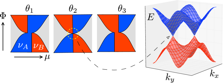
Figure 1: Schematic illustration of a connectivity switch in the quantum Hall phase diagram. Upon variation of a control parameter the connected component switches from topological quantum number to . At the transition a singular point appears in the phase boundary (encircled), associated with gapless Dirac cones in the Brillouin zone (right-most panel).
Here we show that massless Dirac fermions do appear at singular points in the quantum Hall phase diagram, associated with a switch of the phase connectivity upon variation of some control parameter. (See Fig. 1.) Any experimentally accessible quantity that couples to the superlattice potential can play the role of control parameter, in what follows we will consider the angle of crystallographic alignment between graphene and substrate. We find that the phase boundaries separating regions of distinct Hall conductance rearrange their connectivity upon variation of , switching the connected component of the phase diagram from to . In the magnetic Brillouin zone this transition produces a pair of -fold degenerate conical singularities (Dirac points), with massless Dirac fermions as low-energy excitations.
We base our analysis on the moiré superlattice Hamiltonian of Wallbank et al.Wal13 . Starting point is the Dirac Hamiltonian of graphene Cas09 ; Kat12 ,
(1)
for conduction electrons near each of two opposite corners (valleys) of the hexagonal Brillouin zone note1 . The Fermi velocity is and the lattice constant of the hexagonal lattice of carbon atoms is . The momentum in the plane is coupled to pseudospin Pauli matrices and acting on the sublattice degree of freedom. The real spin plays no role and is ignored note2 , only the orbital effect of a perpendicular magnetic field is included (via the vector potential ). The electrostatic potential is adjustable via a gate voltage. For simplicity we assume that the mean free path for impurity scattering is sufficiently large that disorder effects can be neglected.
The moiré effect from a substrate of hexagonal boron nitride (hBN, lattice constant , , misaligned by ) adds superlattice terms to the Dirac Hamiltonian. The terms that break inversion symmetry are small and we neglect them, following Ref. Abe13 . Three terms remain Wal13 ,
(2)
where in the two valleys and
(3)
(4)
The reciprocal lattice vectors have length and are rotated by the matrix
(5)
The periodicity of the superlattice is .
The terms and in the Hamiltonian (2) represent a potential modulation, while the term is a modulation of the hopping amplitudes. The coefficients are related by Kin12 ; Wal13
(6)
where is an energy scale that sets the coupling strength of graphene to the hBN substrate. We use the estimate from Ref. Abe13 , corresponding to a ratio .
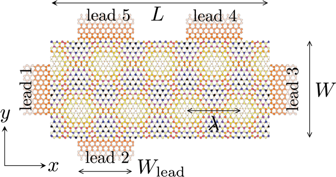
Figure 2: Five-terminal geometry used to calculate the Hall conductivity (7). The two-dimensional hexagonal lattice of the tight-binding model is shown, with the superlattice potential indicated by colored sites and bonds (not to scale, the actual lattice is much finer).
We study electrical conduction in the five-terminal Hall bar geometry of Fig. 2, where a current flows from source 1 to drain 3 while contacts 2, 4, and 5 draw no current. The voltages at these contacts determine the Hall conductivity,
(7)
In linear response and at zero temperature the voltage differences are obtained from the scattering matrix at the Fermi level , which we calculate by discretizing the Hamiltonian (2) on a tight-binding lattice (hexagonal symmetry, lattice constant ). The metallic contacts are modeled by heavily doped graphene leads (infinite length, width , potential ), without the superlattice ( in the leads) and without magnetic field. In the superlattice region (length , width ) we set . (The sign of is chosen such that the Fermi level lies in the conduction band of graphene for and in the valence band for .) We calculate as a function of and using the kwant tight-binding code kwant ; note3 . Results are shown in Fig. 3.
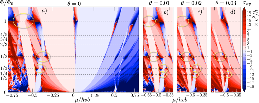
Figure 3: Numerical results for the Hall conductivity of graphene on hBN, calculated in the Hall bar geometry of Fig. 2 for the superlattice Hamiltonian (2). Panel a is for a perfectly aligned substrate, when the flux-induced Dirac cones (encircled) are all gapped. Panels b,c,d show the connectivity switches induced by a slight crystallographic misalignment of the substrate (angle in radians).
Panel 3a shows the known spectral features of the graphene superlattice Pon13 ; Dea13 ; Hun13 ; Che13 : A parabolic fan of Landau levels emerging from the primary zero-field Dirac cone of graphene; secondary zero-field Dirac cones centered at ; and gapped tertiary Dirac cones at flux in a region near (in the valence band only, electron-hole symmetry is strongly broken by the superlattice potential). The phases that meet at these rational flux values have Hall conductance differing by — reflecting a two-fold valley degeneracy and a -fold degeneracy of the magnetic minibands. (We are not counting spin.)
Panels 3b–d show how the connectivity switches from Fig. 1 appear in the numerical simulation when we slightly misalign the hBN lattice relative to the graphene lattice. Each switch in the connected component of the phase diagram is associated with the closing and reopening of the Dirac cones in the magnetic Brillouin zone. (The gap closing at is the one shown in Fig. 1.)
We will now demonstrate that transport properties near these connectivity switches have the characteristics of massless Dirac fermions Bee08 . The effects we consider are the scale-invariant (pseudodiffusive) two-terminal conductivity and sub-Poissonian shot noise at the Dirac point Kat06a ; Two06 , and Klein tunneling through a potential step Kat06b ; Che06 .
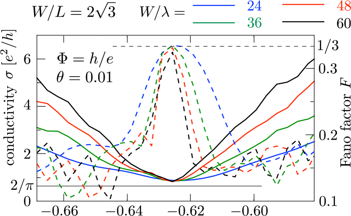
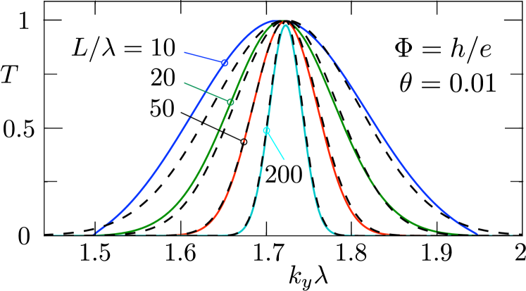
Figure 4: Electrostatic potential profile in a graphene strip, used to study the scale invariant conductivity (panel a, , varying ) and Klein tunneling (panel b, , ). The Fermi level lines up with the flux-induced Dirac point when .
Figure 5: Conductivity (solid curves, left axis) and Fano factor (dashed curves, right axis) calculated in the two-terminal graphene strip of Fig. 4a, for different system sizes at fixed aspect ratio . The scale invariance at signals the appearance of massless Dirac fermions at flux through the superlattice unit cell. The horizontal solid and dashed lines indicate the limits (9) expected from the Dirac equation.
To search for scale invariance we take an infinitely long graphene strip of width , with the potential profile shown in Fig. 4a. The superlattice potential is imposed over a length (where ), while the leads have no superlattice (). The two-terminal conductivity and Fano factor (ratio of noise power and current) are obtained from the transmission eigenvalues ,
(8)
For gapless Dirac cones we expect at the Dirac point the scale invariant values Kat06a ; Two06
(9)
We vary at fixed aspect ratio to search for this scale invariance. We have examined several flux values, here we show representative results for (so ). From Fig. 3 we infer that the connectivity switch at this flux value happens near and . Indeed, in Fig. 5 both and become approximately independent of sample size near these parameter values. The limiting Fano factor is close to the expected ; the limiting conductivity is a bit larger than the expected value, which we attribute to an additional contribution of order from edge states.
Figure 6: Transmission probability through the potential step of Fig. 4b, as a function of transverse wave vector for different step lengths . The flux-induced Dirac point is at . The solid curves result from the numerical simulation of the graphene superlattice at , , the dashed curves are the analytical prediction (11) for Klein tunneling of massless Dirac fermions. (There is no fit parameter in this comparison.)
Klein tunneling is the transmission with unit probability at normal incidence on a potential step that crosses the Dirac point. It is a direct manifestation of the chirality of massless Dirac fermions Kat06b . We search for this effect using the potential profile of Fig. 4b, which for and is symmetrically arranged around the flux-induced Dirac point. In order to avoid spurious reflections from the leads we now apply the superlattice potential and the magnetic field to an unbounded graphene plane. We calculate the transmission probability as a function of transverse wave vector in the magnetic Brillouin zone.
The dependence on the angle of incidence of the transmission probability of massless Dirac fermions depends exponentially on the step length Che06 ,
(10)
for a symmetric junction with the same Fermi momentum at both sides of the potential step. (The step should be smooth on the scale of the lattice constant, so is assumed.) The transverse momentum appearing in the Dirac equation is measured from the Dirac point, . (The flux creates two Dirac cones, both with the same value of .) Inspection of the band structure gives and Fermi velocity , nearly twice the native Fermi velocity of graphene. The angle of incidence then follows from , with , so we expect a transmission peak described by
(11)
The resulting curves are shown in Fig. 6 (dashed curves), for different values of . There is a good agreement with the numerical simulations (solid curves).
The angle-resolved detection in these simulations is convenient to directly access the strongly peaked transmission profile (11). Experimentally this signature of Klein tunneling can be observed without requiring angular resolution in a double potential step geometry You09 .
In summary, we have identified a mechanism for the production of massless Dirac fermions in the Hofstadter butterfly spectrum of a moiré superlattice. Generically, the flux-induced clones of the zero-field Dirac cones are gapped, but the gap closes at a switch in the connected component of the quantum Hall phase diagram. We have presented a model calculation for graphene on an hexagonal boron nitride surface that exhibits these connectivity switches upon variation of the crystallographic misalignment. Only a slight misalignment is needed, on the order of , comparable to what has been realized in experiments Pon13 ; Dea13 ; Hun13 ; Woo14 . Numerical simulations of transport properties at unit flux through the superlattice unit cell reveal the scale invariant conductivity and Klein tunneling that are the characteristic signatures of ballistic transport of massless Dirac fermions. These should be observable in small samples, in larger samples the effects of disorder remain as an interesting problem for further research.
This research was supported by the Foundation for Fundamental Research on Matter (FOM), the Netherlands Organization for Scientific Research (NWO/OCW), an ERC Synergy Grant, and the German Academic Exchange Service (DAAD).
References
(1) D. Hofstadter, Phys. Rev. B 14, 2239 (1976).
(2) D. Osadchy and J. E. Avron, J. Math. Phys. 42, 5665 (2001).
(3) L. A. Ponomarenko, R. V. Gorbachev, G. L. Yu, D. C. Elias, R. Jalil, A. A. Patel, A. Mishchenko, A. S. Mayorov, C. R. Woods, J. R. Wallbank, M. Mucha-Kruczynski, B. A. Piot, M. Potemski, I. V. Grigorieva, K. S. Novoselov, F. Guinea, V. I. Fal ko , and A. K. Geim, Nature 497, 594 (2013).
(4) C. R. Dean, L. Wang, P. Maher, C. Forsythe, F. Ghahari, Y. Gao, J. Katoch, M. Ishigami, P. Moon, M. Koshino, T. Taniguchi, K. Watanabe, K. L. Shepard, J. Hone, and P. Kim, Nature 497, 598 (2013).
(5) B. Hunt, J. D. Sanchez-Yamagishi, A. F. Young, K. Watanabe, T. Taniguchi, P. Moon, M. Koshino, P. Jarillo-Herrero, and R. C. Ashoori, Science 340, 1427 (2013).
(6) R. Rammal, J. Physique 46, 1345 (1985).
(7) J.-M. Hou, W.-X. Yang, and X.-J. Liu, Phys. Rev. A 79, 043621 (2009).
(8) F. Gerbier and J. Dalibard, New J. Phys. 12, 033007 (2010).
(9) P. Delplace and G. Montambaux, Phys. Rev. B 82, 035438 (2010).
(10) J.-W. Rhim and K. Park, Phys. Rev. B 86, 235411 (2012).
(11) B. Sachs, T. O. Wehling, M. I. Katsnelson, and A. I. Lichtenstein, Phys. Rev. B 84, 195414 (2011).
(12) C. Ortix, L. Yang, and J. van den Brink, Phys. Rev. B 86, 081405(R) (2012).
(13) M. Yankowitz, J. Xue, D. Cormode, J. D. Sanchez-Yamagishi, K. Watanabe, T. Taniguchi, P. Jarillo-Herrero, P. Jacquod, and B. J. LeRoy, Nature Phys. 8, 382 (2012).
(14) M. Kindermann, B. Uchoa, and D. L. Miller, Phys. Rev. B 86, 115415 (2012).
(15) X. Chen, J. R. Wallbank, A. A. Patel, M. Mucha-Kruczyński, E. McCann, and V. I. Fal’ko, arXiv:1310.8578.
(16) J. R. Wallbank, A. A. Patel,, M. Mucha-Kruczyński, A. K. Geim, and V. I. Fal’ko, Phys. Rev. B 87, 245408 (2013).
(17) A. H. Castro Neto, F. Guinea, N. M. R. Peres, K. S. Novoselov, and A. K. Geim, Rev. Mod. Phys. 81, 109 (2009).
(18) M. I. Katsnelson, Graphene: Carbon in Two Dimensions (Cambridge University Press, 2012).
(19) The valley-isotropic Dirac Hamiltonian (1) acts on the spinor in valley and in valley , where are the wave amplitudes on the two triangular sublattices that form the hexagonal lattice of graphene.
(20) Because the spin degree of freedom is not counted, the conductance quantum is rather than .
(21) D. S. L. Abergel, J. R. Wallbank, X. Chen, M. Mucha-Kruczyński, and V. I. Fal’ko, New J. Phys. 15, 123009 (2013).
(22) C. W. Groth, M. Wimmer, A. R. Akhmerov, and X. Waintal, arXiv:1309.2926.
(23) Details of the calculation are given in the Appendix.
(24) C. W. J. Beenakker, Rev. Mod. Phys. 80, 1337 (2008).
(25) M. I. Katsnelson, Eur. Phys. J. B 51, 157 (2006).
(26) J. Tworzydło, B. Trauzettel, M. Titov, A. Rycerz, and C. W. J. Beenakker, Phys. Rev. Lett. 96, 246802 (2006).
(27) M. I. Katsnelson, K. S. Novoselov, and A. K. Geim, Nature Phys. 2, 620 (2006).
(28) V. V. Cheianov and V. I. Fal’ko, Phys. Rev. B, 74, 041403 (2006).
(29) A. F. Young and P. Kim, Nature Physics 5, 222 (2009).
(30) C. R. Woods, L. Britnell, A. Eckmann, G. L. Yu, R. V. Gorbachev, A. V. Kretinin, J. Park, L. A. Ponomarenko, M. I. Katsnelson, Yu. N. Gornostyrev, K. Watanabe, T. Taniguchi, C. Casiraghi, A. K. Geim, and K. S. Novoselov, arXiv:1401.2637.
Appendix A Derivation of the tight-binding Hamiltonian for the moiré superlattice
Our numerical simulations are based on a tight-binding discretization of the moiré superlattice Hamiltonian (2) for graphene on an hexagonal substrate. Here we provide a derivation of the tight-binding Hamiltonian, arriving at Eq. (28). This is not quite straightforward, because of the need to accomodate two lattices, of graphene and of the substrate, in a single discretization. We start with zero magnetic field ().
In order to achieve a commensurate discretization of the bare graphene Hamiltonian (1) and the moiré superlattice defined by reciprocal lattice vectors , for arbitrary alignment angle , we make use of the invariance of under a simultaneous rotation of space and pseudospin (sublattice degree of freedom).
A rotation by
(12)
leaves invariant,
(13)
while bringing the reciprocal lattice vectors in alignment with .
The first two terms of the moiré modulation transform into
(14)
(15)
(16)
The rotated reciprocal superlattice vectors
(17)
depend on only in their length , but unlike not in their direction.
The third term of the moiré modulation transforms into
(18)
We have introduced the fictitious vector potential
(19)
The full Hamiltonian in the rotated basis reads
(20)
In the following we will work in this rotated basis, but in favor of a simple notation we will drop the tilde .
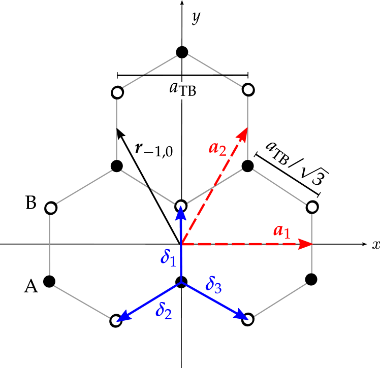
Figure 7: Hexagonal lattice of the tight-binding model, with lattice vectors , and nearest-neighbor displacement vectors , , . The two sublattices have sites labeled A (filled dots) and B (open dots). The vector denotes the center of unit cell .
We discretize the Hamiltonian (20) in the rotated basis on the hexagonal lattice, defined by the lattice vectors
(21)
and the three nearest neighbor displacement vectors
(22)
The vector , with integer, denotes the center of unit cell .
As shown in Fig. 7 we put the sites belonging to the A(B)-sublattice at to have inversion symmetry about the origin.
To ensure that the discretization (lattice constant ) is commensurate with the moiré superlattice (lattice constant ), we take an integer ratio , so
(23)
The accuracy of the discretization is improved by increasing . (In the simulations we take .)
The bare graphene Hamiltonian (13) is produced by nearest-neighbor hopping on the hexagonal lattice,
(24)
Here denotes the positions of sites on sublattice A, and are creation operators on the A and B sites, and is the hopping amplitude,
(25)
The superlattice term in Eq. (14) corresponds to a periodic spatial modulation of the on-site energy, the same for A and B sites, while the term has an additional staggering — acting on A and B sites with opposite sign. To maintain the spatial inversion symmetry of the continuum model we evaluate both terms at the center of each unit cell. The resulting terms are given in Eqs. (29) and (30).
The superlattice term with the fictitious vector potential in Eq. (18) represents a periodic spatial modulation of the nearest-neighbor hopping amplitudes in the tight-binding Hamiltonian (24). The replacement produces in the continuum limit the vector potential Cas09
(26)
The vectors and locate the two Dirac cones (valleys) in the hexagonal Brillouin zone.
We seek to discretize a given fictitious vector potential on the lattice, in other words we need to invert (26).
The complex field is constructed from three real hoppings, so we have some freedom in choosing the .
We take
(27)
To avoid a spurious breaking of inversion symmetry we evaluate in the middle of each bond, rather than on the lattice site.
Collecting results, we arrive at the tight-binding Hamiltonian
(28)
The energies
(29)
(30)
correspond to the periodic on-site contributions of the moiré super-lattice potential which are symmetric () and antisymmetrc () with respect to a swap of the A and B sublattice.
The hoppings
(31a)
(31b)
(31c)
include both the isotropic contribution of native graphene and the periodic modulation from the moiré superlattice, produced by the fictitious vector potential
(32)
Finally, the orbital effect of the magnetic field is included by adding a Peierls phase to the hopping amplitude , where is the flux through the superlattice unit cell.